US8097080B2 - Method of cutting single crystals - Google Patents
Method of cutting single crystals Download PDFInfo
- Publication number
- US8097080B2 US8097080B2 US12/271,245 US27124508A US8097080B2 US 8097080 B2 US8097080 B2 US 8097080B2 US 27124508 A US27124508 A US 27124508A US 8097080 B2 US8097080 B2 US 8097080B2
- Authority
- US
- United States
- Prior art keywords
- crack
- stress
- cleavage
- energy
- propagation
- Prior art date
- Legal status (The legal status is an assumption and is not a legal conclusion. Google has not performed a legal analysis and makes no representation as to the accuracy of the status listed.)
- Active, expires
Links
Images


Classifications
-
- H—ELECTRICITY
- H10—SEMICONDUCTOR DEVICES; ELECTRIC SOLID-STATE DEVICES NOT OTHERWISE PROVIDED FOR
- H10P—GENERIC PROCESSES OR APPARATUS FOR THE MANUFACTURE OR TREATMENT OF DEVICES COVERED BY CLASS H10
- H10P54/00—Cutting or separating of wafers, substrates or parts of devices
-
- B—PERFORMING OPERATIONS; TRANSPORTING
- B28—WORKING CEMENT, CLAY, OR STONE
- B28D—WORKING STONE OR STONE-LIKE MATERIALS
- B28D5/00—Fine working of gems, jewels, crystals, e.g. of semiconductor material; apparatus or devices therefor
-
- B—PERFORMING OPERATIONS; TRANSPORTING
- B28—WORKING CEMENT, CLAY, OR STONE
- B28D—WORKING STONE OR STONE-LIKE MATERIALS
- B28D5/00—Fine working of gems, jewels, crystals, e.g. of semiconductor material; apparatus or devices therefor
- B28D5/0058—Accessories specially adapted for use with machines for fine working of gems, jewels, crystals, e.g. of semiconductor material
- B28D5/0064—Devices for the automatic drive or the program control of the machines
-
- Y—GENERAL TAGGING OF NEW TECHNOLOGICAL DEVELOPMENTS; GENERAL TAGGING OF CROSS-SECTIONAL TECHNOLOGIES SPANNING OVER SEVERAL SECTIONS OF THE IPC; TECHNICAL SUBJECTS COVERED BY FORMER USPC CROSS-REFERENCE ART COLLECTIONS [XRACs] AND DIGESTS
- Y10—TECHNICAL SUBJECTS COVERED BY FORMER USPC
- Y10S—TECHNICAL SUBJECTS COVERED BY FORMER USPC CROSS-REFERENCE ART COLLECTIONS [XRACs] AND DIGESTS
- Y10S117/00—Single-crystal, oriented-crystal, and epitaxy growth processes; non-coating apparatus therefor
- Y10S117/915—Separating from substrate
-
- Y—GENERAL TAGGING OF NEW TECHNOLOGICAL DEVELOPMENTS; GENERAL TAGGING OF CROSS-SECTIONAL TECHNOLOGIES SPANNING OVER SEVERAL SECTIONS OF THE IPC; TECHNICAL SUBJECTS COVERED BY FORMER USPC CROSS-REFERENCE ART COLLECTIONS [XRACs] AND DIGESTS
- Y10—TECHNICAL SUBJECTS COVERED BY FORMER USPC
- Y10T—TECHNICAL SUBJECTS COVERED BY FORMER US CLASSIFICATION
- Y10T225/00—Severing by tearing or breaking
- Y10T225/10—Methods
- Y10T225/12—With preliminary weakening
-
- Y—GENERAL TAGGING OF NEW TECHNOLOGICAL DEVELOPMENTS; GENERAL TAGGING OF CROSS-SECTIONAL TECHNOLOGIES SPANNING OVER SEVERAL SECTIONS OF THE IPC; TECHNICAL SUBJECTS COVERED BY FORMER USPC CROSS-REFERENCE ART COLLECTIONS [XRACs] AND DIGESTS
- Y10—TECHNICAL SUBJECTS COVERED BY FORMER USPC
- Y10T—TECHNICAL SUBJECTS COVERED BY FORMER US CLASSIFICATION
- Y10T428/00—Stock material or miscellaneous articles
- Y10T428/24—Structurally defined web or sheet [e.g., overall dimension, etc.]
- Y10T428/24802—Discontinuous or differential coating, impregnation or bond [e.g., artwork, printing, retouched photograph, etc.]
-
- Y—GENERAL TAGGING OF NEW TECHNOLOGICAL DEVELOPMENTS; GENERAL TAGGING OF CROSS-SECTIONAL TECHNOLOGIES SPANNING OVER SEVERAL SECTIONS OF THE IPC; TECHNICAL SUBJECTS COVERED BY FORMER USPC CROSS-REFERENCE ART COLLECTIONS [XRACs] AND DIGESTS
- Y10—TECHNICAL SUBJECTS COVERED BY FORMER USPC
- Y10T—TECHNICAL SUBJECTS COVERED BY FORMER US CLASSIFICATION
- Y10T428/00—Stock material or miscellaneous articles
- Y10T428/31504—Composite [nonstructural laminate]
- Y10T428/31678—Of metal
Definitions
- the invention relates to a method of separating single crystals, e.g., single crystalline plates or wafers or parts thereof.
- the application relates to a method of dividing single crystals including a crack propagation that is self-adjusting.
- Single crystalline wafers comprising semiconducting materials are used as substrates for the manufacturing of micro-electronic components such as field effect or hetero-bipolar transistors, and of opto-electronic components, such as laser or luminescence diodes.
- micro-electronic components such as field effect or hetero-bipolar transistors
- opto-electronic components such as laser or luminescence diodes.
- the functional layers are deposited and optionally reworked upon those substrates, or are generated within the substrate by means of ion implantation. These substrates then run through complex structuring processes undergoing multiple applications of exposure masks.
- the substrate For the purpose of orientation (adjustment) of the exposure masks and optionally for the necessary distinction between a front face and a rear face of the substrate, the substrate comprises a so-called orientation flat (OF) and an identification flat (IF), which is offset with regard to the orientation flat by 90° in the clockwise or counter-clockwise direction.
- OF orientation flat
- IF identification flat
- the wafer normal and the surface normal of the flats are generally perpendicular with respect to each other.
- Conventional manufacturing processes of wafers having flats include the generation of the flats by means of grinding.
- the adjustment accuracy of the orientation flats with regard to the crystallographic ⁇ 110>-direction may amount to ⁇ 1°, for the identification flat ⁇ 5°, in case of a conventional wafer manufacturing, but values even up to ⁇ 0.02° may be achieved for the orientation flat employing the above method.
- Flats manufactured by grinding may comprise mis-orientations fluctuating along the flats as well as chips at the edges, which affect the function of the flats as references for the adjustment of exposure masks. This is particularly valid in the case of manufacturing laser diodes, which necessitate high precision and further undisturbed, sharp-edged flats having an adjustment accuracy of ⁇
- the orientation accuracy of the flats can be increased, if these are generated by cleaving the generally brittle semiconductor materials instead of grinding the flats, thereby employing natural cleavage planes.
- the ⁇ 110 ⁇ -planes are natural cleavage planes.
- U.S. Pat. Nos. 5,279,077 and 5,439,723 there are known wafers provided with flats generated by such cleaving accordingly.
- U.S. Pat. No. 5,154,333 there is known a cleaving device, which is used to carry out cleavage with a predefined bending stress of a wafer, which contains a seed crack generated by scribing the wafer.
- a disadvantage of the mechanical cleaving device arises in that the crack progress can not be controlled, and in that due to the initialization of the breakage by means of a seed break at the wafer edge a complex fracture mode is realized.
- a basic method relates to a process of cutting flat glass by means of thermally induced stress which is described in DE 28 13 302. According to this method glass is heated in one area and cooled in another area, both areas being provided on the glass on at least one of its two main faces and being placed one after the other on the intended straight cutting line, and further being sharply delineated and symmetric with respect to the cutting line. Temperature gradients result in the glass along the thickness direction and in the direction of the scribe line. The temperature gradients cause thermal stress, which starting from the initial crack at the edge drives a crack perpendicular to the main faces and along the predetermined straight cutting line. Therein the crack progress velocity can be controlled by regulating the applied temperatures and the feeding of the heating and cooling device.
- One feature of known methods of dividing brittle materials by propagating a crack is the generation or the presence of an initial crack.
- a stress field is generated using a suitable method such as, e.g., the above mentioned mechanical bending stress, or by applying a thermal load.
- This stress field leads to a complex load at the propagation front of the crack, which may be characterized by a stress-intensity factor K.
- K the stress-intensity factor
- the crack propagation proceeds according to the principle of minimizing the free energy of the body that is to be divided. This means, that the crack propagates such that in isotropic materials the mechanical-energy-release rate G becomes a maximum.
- anisotropic materials a principle of minimizing the effective surface energy 2 ⁇ e of the divided surfaces competes with the principle of maximizing the rate of the mechanical energy release when minimizing the total energy of the system during the crack propagation.
- cleavage planes having accuracies in the range of ⁇
- the area relevant for the respective technology corresponds in the case of laser diodes for example with a length of a laser resonator, or in the case of integrated circuits with the edge length of a chip to be separated. Upon separation of material in order to form flats it corresponds to the flat length. Also, the manufacturing of a natural cleavage plane along the crystallographic grid plane becomes possible due to the self-adjusted cleaving proposed herein.
- the orientation accuracy of a separation surface of the single crystal with respect to a crystallographic grid plane is measured by aligning the crystal with a reference face, wherein at least two points of the separation surface abut on the reference face. Using an X-ray goniometer the orientation of the crystallographic grid plane can then be determined with respect to this reference plane. The grid plane orientation is then related to the reference surface plane resulting in an angle difference, which herein represents the accuracy.
- the orientation of the separation surface with respect to the reference surface according to the method used for determining the grid plane orientation can also be obtained by following different approaches as compared with the above described mechanical abutment, e.g., by applying optical methods.
- a local orientation difference can also be obtained by sub-dividing this technologically relevant surface length into portions of, e.g., 2 mm and performing the orientation measurement using for example an optical microscope, a miniature interferometer, a white light interferometer or an autocollimator. The orientation accuracy then corresponds to the largest of these measured local differences.
- the cleavage planes that may be obtained according to certain embodiments of the present invention are distinguishable as such from surfaces of semiconductor plates having another orientation when known measurement methods are applied such as the LEED method (low energy electron diffraction), cf. Qian, G. X., Martin, R. M., Chadi, D. J., in Phys. Rev. B, Vol. 37, p. 1303. (1988), or Bechstedt, F. “Principles of Surface Physics”, Springer Verlag, Berlin, ISBN 978-3-540-00635-0, Chapter 1.2.4; pages 16-18.
- LEED method low energy electron diffraction
- cf. Qian low energy electron diffraction
- G. X. Martin
- R. M. Chadi, D. J., in Phys. Rev. B, Vol. 37, p. 1303. (1988)
- Bechstedt F. “Principles of Surface Physics”, Springer Verlag, Berlin, ISBN 978-3-540-00635-0
- the method has the advantage that the previous determination and adjustment of the crystallographic cleavage planes for the cleavage device are required only with common accuracies.
- the precise orientation of the propagating crack is facilitated by the process conditions according to certain embodiments of the invention, which enforce a self-adjustment of the direction of crack propagation in precisely one of the crystallographic cleavage planes without steps or jumps.
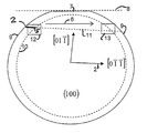
- FIG. 1 shows a schematical top view of a wafer to be cleaved
- FIG. 2 shows the mechanical-energy-release rate G and the effective surface energy 2 ⁇ e upon compliance with a first condition
- FIG. 3 shows the mechanical-energy-release rate G and the effective surface energy 2 ⁇ e upon compliance with a second condition
- FIG. 4 shows the mechanical-energy-release rate G and the effective surface energy 2 ⁇ e upon compliance with a third condition
- FIG. 5 shows the mechanical-energy-release rate G and the effective surface energy 2 ⁇ e upon compliance with a fourth condition
- FIG. 6 shows a first phase of crack propagation
- FIG. 7 shows a second phase of crack propagation, which is controlled by the relative movement of the stress fields (e.g., in isotropic materials);
- FIG. 8 shows a phase of crack propagation in the case of a deviation from the desired cleavage direction when a crystallographic cleavage plane is present and when the stress fields are asymmetrically adjusted with respect to the cleavage plane;
- FIG. 9 shows a phase of crack propagation in a desired cleavage direction in the case of an ideal symmetrical adjustment of the stress fields with respect to the cleavage plane
- FIG. 10 shows a schematical representation of the orientation of a GaAs-wafer in the cleavage device
- FIG. 11 shows an example of the maximum error consisting of a deviation of the position and direction between the desired cleavage plane and the movement direction as well as the generated stress fields in the start region;
- FIG. 12 shows an example of the maximum error consisting of a deviation of the position and direction between the desired cleavage plane and the movement direction as well as the generated stress fields in the target region;
- FIG. 13 shows the mechanical-energy-release rates G ⁇ and G + in the start- and target regions in dependence of angle ⁇ ;
- FIG. 14 shows a phase of crack propagation under compliance with certain conditions.
- the wafer is provided to the cleavage device.
- the adjustment of the wafer with respect to the cleavage device is performed by virtue of a previously formed marking, e.g., a short flat, which by means of example is grinded and oriented by means of X-ray diffractometry.
- a previously formed marking e.g., a short flat
- a pre-adjustment means may be considered as pre-adjustment means.
- the pre-adjustment with respect to the movement direction may be carried out with the help of stops or employing optical methods.
- an initial crack 2 is formed in a ⁇ 110 ⁇ -cleavage plane of the GaAs-wafer 1 .
- the initial crack 2 is formed in a cleavage plane which is parallel to a preferred gliding direction of the ⁇ -dislocations.
- the initial crack 2 is for example generated by an indenter with defined geometry (Vickers, Knoop-indenter). Similarly, other geometries or a scoring of the surface are possible. By proper selection of the indentation load and geometry the formation of B-cracks perpendicular thereto can be avoided.
- a plane edge-crack extending to the wafer backside is generated from the indentation-induced crack in the ⁇ 110 ⁇ -cleavage plane.
- This edge-crack serves as a plane initial crack for the further crack propagation, or for the desired cleavage direction, or for the cleavage plane 2 ′, respectively.
- the thermally induced stress fields are dimensioned, such that the initial crack can not yet propagate further in this phase.
- a stress intensity K is generated for the purpose of crack propagation, and the quantity G( ⁇ ) is determined, which represents the rate of energy release upon further crack propagation in dependence of a deflection of the crack from the cleavage plane about an angle ⁇ .
- the crack propagation may be regarded as a superposition of a twist (twist configuration) about the angle ⁇ around an axis perpendicular to the crack front of the initial crack and a rotation about an angle ⁇ around an axis in the crack front of the initial crack (tilt configuration). Both cases can be considered separately.
- the embodiment is detailed with regard to the example of the tilt-configuration without restricting the validity of the general case.
- the stress intensity K is generated by employing known methods such as for example the method according to DE 28 13 302 or the method according to WO 93/20015.
- one or more heat sources 4 as well as one or more heat sinks 3 are localized on one or both wafer faces, such that ideal symmetrical stress fields are obtained with respect to the wafer thickness as well as with respect to the desired cleavage direction.
- the heat sources can be generated for example by absorption of laser light, and the heat sinks can be generated by an application of cooling aerosols such as described for example in WO 93/20015. Similarly, other variants are possible as well.
- the heat sources and heat sinks are controlled and positioned such that a crack propagation is enabled.
- the temperature has to be sufficiently low in order to avoid plastic deformations. For GaAs a temperature of less than about 300° C. is considered as being appropriate.
- the dimensioning or control, or even a feedback control, of the stress fields is carried out, such that crack propagation occurs continually or in intervals, wherein crack propagation is characterized by G(0) ⁇ 2 ⁇ e (0).
- the dimensioning or control of the stress fields is performed such that at least one of the following conditions is satisfied:
- the effective free surface energy ⁇ e which is used in fracture mechanics, is determined in breakage experiments from a relation between fracture strength and crack length. This quantity further contains—as compared with the intrinsic surface energy ⁇ s —energy portions of dissipative processes. To these belong—among others—the formation of dislocations in the process zone or plastic zone, the emission of acoustic energy or the occurrence of dissipative structures (fracture structures) at the fracture surfaces. Hence, the surface energy ⁇ e is larger than the intrinsic surface energy ⁇ s .
- k B denotes the Boltzmann constant
- ⁇ denotes the binding energy between closest neighbours in the crystal lattice
- a denotes the distance between building units within the step.
- the binding energy ⁇ can be estimated from the sublimation energy ⁇ H sub (T) of the crystal (“congruent vaporization”) and the coordination number Z of the considered crystal: ⁇ H sub /Z, wherein ⁇ H sub (T) is obtained from a calculation of the thermo-dynamic equilibrium X s X g with the thermo-dynamic data of the solid (s) and the gaseous (g) phase X.
- the free step energy can also be determined experimentally.
- the free step energy becomes: ⁇ e ⁇ 3.31 ⁇ 10 ⁇ 10 J/m, and ⁇ e /h ⁇ 0.83 J/m 2 .
- step energy For the free step energy the same conclusions as for the surface energy may analogously be derived.
- the effective step energy experimentally derived can be larger than the step energy estimated herein due to dissipative portions.
- step energy By indicating the theoretically obtained step energy, the right side in conditions (2.1) and (2.2) is known.
- Stress fields can be calculated obeying the conditions of the heat sources and sinks by employing simulation calculations. But also direct measurement of the stress is possible, for example via stress birefringence, ultrasonic microscopy, micro-Raman-spectroscopy etc. Thereof, the mechanical-energy-release rate G is calculated for the preset stress field in dependence from possible deflections of the crack about angle ⁇ . By controlling and positioning the heat sources and sinks, the stress fields are adjusted, such that the above mentioned conditions are satisfied.
- an angular range ⁇ 1 ⁇ 2 exists, in which the condition G ⁇ 2 ⁇ e is satisfied.
- This range depends on the stress fields and the material characteristics as well as on the misorientation of the employed cleavage device from the targeted cleavage plane.
- the necessary condition (1.1) for the crack propagation is satisfied.
- the control according to the certain embodiments of the invention, or the dimensioning of the stress intensity K aiming at a compliance with conditions (2.1) or (2.2) facilitates, that the crack is not deflected in the angular range ⁇ 1 ⁇ 2 , rather it moves over the complete separation distance within the targeted cleavage plane.
- the crack propagation is enforced in a desired lattice plane by self-adjustment of the crack propagation direction.
- can be generated.
- cleavage surfaces having a minimum step density, ideally without steps, can be produced within the complete technologically relevant area (flats, resonator surfaces, etc.).
- FIGS. 2 and 3 Two situations, in which the conditions according to certain embodiments of the invention are satisfied, are illustrated in FIGS. 2 and 3 .
- surfaces such as for example flats having an orientation accuracy of 0.01°—as measured over the surface range relevant for this technology—can be applied to a wafer, i.e., an accuracy commonly achieved in practice by a grinding process can be increased by one order of magnitude.
- the method ensures that the adjustment accuracy between the movement direction and the cleavage plane of 0.1° is sufficient in order to constrain the crack propagation in the cleavage plane with an accuracy of ⁇ 0.01°.
- First results show that accuracies of even ⁇ 0.005° or ⁇ 0.001° may be obtained.
- a completely stepless ideal cleavage surface can be obtained which extends precisely along the natural crystallographic plane.
- FIGS. 4 and 5 show situations, in which the mis-orientation of the cleavage device, or a stress intensity K with mixed crack opening modes is present and the conditions according to certain embodiments of the invention are not satisfied.
- FIGS. 6 to 9 show different cases of crack propagation in the wafer.
- a compression stress maximum 4 ′ and a tensile stress maximum 3 ′ is generated.
- the heat sources and sinks are positioned such as to locate the compression stress maximum 4 ′ in front of the crack tip 5 in the propagation direction, and the tensile stress maximum 3 ′ behind the crack tip 5 , as shown in FIG. 6 .
- the conditions (1.1) K>K C or G>2 ⁇ e , or (1.2) K ⁇ K C or G ⁇ 2 ⁇ e can be controlled.
- the crack tip 5 can be advanced, stopped or further moved as desired.
- the relative movement can be carried out by a movement of the heat sources and heat sinks (laser focus or cooling nozzles, respectively), or it can be carried out by a movement of the wafer, or it can be carried out by a combination of both.
- Dissipative or dynamical effects can be avoided by controlling the propagation velocity.
- the propagation velocity can be selected to sufficiently small values, such that a quasi static crack propagation at thermo-dynamic equilibrium can be assumed (v ⁇ 1 ⁇ 3 of the sound velocity).
- the crack propagation follows the relative movement 6 between the stress fields and the wafer 1 . This is utilized in prior art, in order to cut complicated geometries, which may be straight or curved.
- FIG. 10 shows the orientation of the GaAs-wafer 1 in the cleavage device.
- a marking or short flat 7 is commonly present, which is grinded with a predetermined orientation tolerance with respect to the crystallographic directions. Thereby, under practical circumstances and with justifiable efforts an accuracy of the flat orientation 8 with respect to the ⁇ 110 ⁇ -cleavage planes of 0.1° is achievable.
- the flat 7 is pre-adjusted with respect to the movement direction 6 of the relative movement between the stress fields and the wafer.
- a surface (flat) is formed on the wafer having an orientation accuracy of ⁇
- the accuracy which in practice can be achieved using a grinding process, has been increased by an order of magnitude.
- the method according to certain embodiments of the invention facilitates that the adjustment accuracy between the movement direction 6 and the cleavage plane 2 ′ of 0.1° suffices to constrain the crack propagation within the cleavage plane to an accuracy of at least ⁇ 0.01°.
- This can be continued from a wafer edge 9 to an opposed wafer edge 9 , or there may be present a predetermined region 10 , within which the requirements to orientation accuracy of the flat 11 to be generated have to be fulfilled.
- the size and geometry of this region 10 may vary and depends on different technological requirements. Accuracies of ⁇ 0.005°
- the stress fields are calculated, preferably with the selected conditions with regard to the heating sources and sinks.
- the simulation is carried out in the regions at the preset start and target points of the dividing process. This can be done for example at the edges of the technologically used region 10 within areas 12 and 13 .
- the initial crack 2 within the cleavage plane at the edge of the start area 12 is present according to the above mentioned methods, preferably outside of region 10 . Also other positions are possible.
- the proportions of FIG. 10 are not drawn to the scale and are shown exaggeratedly for illustration purposes.
- the hitherto known measurement accuracies (for example in X-ray diffractometry), the known tolerances with regard to grinding and the known positional accuracies determine the maximum error upon pre-adjustment of the wafer. For example, it is possible to determine with the help of simple geometrical relations the maximum error between position and direction of the desired cleavage plane and the movement direction 6 and also relative to the generated tensional fields 3 ′ and 4 ′ in the start and target areas 12 and 13 of the separation process.
- FIG. 11 shows an example of the maximum error in the start area 12 .
- FIG. 12 shows an example of the maximum error in the target area 13 . Note that also mirrored positions are possible.
- the mechanical-energy-release rate G can be calculated for the case of infinitesimal crack propagation in dependence from possible deflections about the angle ⁇ for the given stress fields in the start position 12 of the crack tip 5 of the initial crack.
- the same can be calculated in the planned target area 13 under the assumption that the crack has not left the cleavage plane 2 ′.
- G ⁇ ( ⁇ ) and G + ( ⁇ ) which are given by the known maximum error in the start and target positions.
- the true function G( ⁇ ) is not known, but represents a state between G ⁇ ( ⁇ ) and G + ( ⁇ ).
- FIG. 13 shows an example of a balanced situation.
- the calculation of the functions G ⁇ ( ⁇ ) and G + ( ⁇ ) and the balancing of the stress fields can also be carried out iteratively as well as for all possible combinations of known maximum errors due to pre-adjustment.
- the control and dimensioning of the stress fields is in simple fashion possible for example by control of the laser power and/or the variation of laser focus and/or the arrangement of cooling nozzles relative to the laser spot using the known methods. Nevertheless, further alternatives may equally be considered.
- the invention can further be carried such that during the step of testing the conditions (2.1) or (2.2) a maximum admissible range of angles ⁇ 1 ⁇ 2 is determined. In this range
- the determined angular range is then compared with a predetermined mean alignment- or adjustment-error of an orientation of the crystallographic ( 2 ′) relative to the separation device.
- the control of the stress fields ( 3 ′, 4 ′) and/or the adaption of the pre-adjustment of the crystal is then carried out in dependence of the result of the comparison.
- the invention is not limited to the separation of GaAs-wafers, which are described herein as an embodiment. Rather, the invention may also be applied to any single crystal. Approximated values for a CaF 2 (111)-plane are for example
- the invention is also applicable to single crystals, which are formed as single crystalline layers on a single crystalline substrate.
- the layer and the substrate can thereby be formed from the same or a different material composition.
- the propagation of the crack is maintained within a stress filed between the temperature sink and the temperature source.
- the invention is, however, not restricted to that specific arrangement.
- the stress fields can also be provided by the mere presence of a temperature sink or alternatively of a temperature source, and/or the propagation front is maintained in front of the sink and/or source and not behind one of them or between both.
- the invention can further be embodied as a computer program product, which is arranged to perform and control the steps provided in the appended method claims.
Landscapes
- Engineering & Computer Science (AREA)
- Mechanical Engineering (AREA)
- Crystals, And After-Treatments Of Crystals (AREA)
- Processing Of Stones Or Stones Resemblance Materials (AREA)
- Dicing (AREA)
Priority Applications (2)
| Application Number | Priority Date | Filing Date | Title |
|---|---|---|---|
| US12/271,245 US8097080B2 (en) | 2007-11-15 | 2008-11-14 | Method of cutting single crystals |
| US13/226,519 US8723288B2 (en) | 2007-11-15 | 2011-09-07 | Method of cutting single crystals |
Applications Claiming Priority (5)
| Application Number | Priority Date | Filing Date | Title |
|---|---|---|---|
| US99639607P | 2007-11-15 | 2007-11-15 | |
| DE102007056115 | 2007-11-15 | ||
| DE200710056115 DE102007056115A1 (de) | 2007-11-15 | 2007-11-15 | Verfahren zum Trennen von Einkristallen |
| DE102007056115.8 | 2007-11-15 | ||
| US12/271,245 US8097080B2 (en) | 2007-11-15 | 2008-11-14 | Method of cutting single crystals |
Related Child Applications (1)
| Application Number | Title | Priority Date | Filing Date |
|---|---|---|---|
| US13/226,519 Division US8723288B2 (en) | 2007-11-15 | 2011-09-07 | Method of cutting single crystals |
Publications (2)
| Publication Number | Publication Date |
|---|---|
| US20090283761A1 US20090283761A1 (en) | 2009-11-19 |
| US8097080B2 true US8097080B2 (en) | 2012-01-17 |
Family
ID=40560840
Family Applications (2)
| Application Number | Title | Priority Date | Filing Date |
|---|---|---|---|
| US12/271,245 Active 2030-07-14 US8097080B2 (en) | 2007-11-15 | 2008-11-14 | Method of cutting single crystals |
| US13/226,519 Active US8723288B2 (en) | 2007-11-15 | 2011-09-07 | Method of cutting single crystals |
Family Applications After (1)
| Application Number | Title | Priority Date | Filing Date |
|---|---|---|---|
| US13/226,519 Active US8723288B2 (en) | 2007-11-15 | 2011-09-07 | Method of cutting single crystals |
Country Status (7)
| Country | Link |
|---|---|
| US (2) | US8097080B2 (zh) |
| EP (2) | EP2377662A1 (zh) |
| JP (2) | JP5697984B2 (zh) |
| CN (1) | CN101861237B (zh) |
| AT (1) | ATE543622T1 (zh) |
| DE (1) | DE102007056115A1 (zh) |
| WO (1) | WO2009062744A1 (zh) |
Cited By (1)
| Publication number | Priority date | Publication date | Assignee | Title |
|---|---|---|---|---|
| US20100310775A1 (en) * | 2009-06-09 | 2010-12-09 | International Business Machines Corporation | Spalling for a Semiconductor Substrate |
Families Citing this family (10)
| Publication number | Priority date | Publication date | Assignee | Title |
|---|---|---|---|---|
| KR100945506B1 (ko) * | 2007-06-26 | 2010-03-09 | 주식회사 하이닉스반도체 | 웨이퍼 및 이를 이용한 반도체 패키지의 제조 방법 |
| US20160008926A1 (en) * | 2014-07-14 | 2016-01-14 | Rubicon Technology, Inc. | Method of cold-cleaving sapphire material at cryogenic temperatures |
| CN107922259B (zh) * | 2015-09-04 | 2021-05-07 | Agc株式会社 | 玻璃板的制造方法、玻璃板、玻璃物品的制造方法、玻璃物品以及玻璃物品的制造装置 |
| FR3055063B1 (fr) * | 2016-08-11 | 2018-08-31 | Soitec | Procede de transfert d'une couche utile |
| JP6795811B2 (ja) * | 2017-02-16 | 2020-12-02 | 国立大学法人埼玉大学 | 剥離基板製造方法 |
| EP3795855A1 (fr) * | 2019-09-20 | 2021-03-24 | Patek Philippe SA Genève | Procede de realisation d'un ressort horloger en materiau monocristallin et ressort horloger obtenu par ce procede |
| CN111640687B (zh) * | 2020-06-08 | 2023-03-14 | 郑州磨料磨具磨削研究所有限公司 | 一种单晶晶圆最优划片方向的确定方法 |
| DE102020209092A1 (de) * | 2020-07-21 | 2022-01-27 | Sicrystal Gmbh | Kristallstrukturorientierung in Halbleiter-Halbzeugen und Halbleitersubstraten zum Verringern von Sprüngen und Verfahren zum Einstellen von dieser |
| CN112326707B (zh) * | 2020-09-27 | 2024-06-25 | 威科赛乐微电子股份有限公司 | 一种GaAs基晶圆斜切角度的快速表征方法 |
| CN114393723B (zh) * | 2022-01-20 | 2023-06-13 | 中环领先半导体材料有限公司 | 一种实现滚磨设备定位开槽复检自检一体化的方法 |
Citations (11)
| Publication number | Priority date | Publication date | Assignee | Title |
|---|---|---|---|---|
| DE2813302B1 (de) | 1978-03-28 | 1979-01-11 | Fraunhofer Ges Forschung | Verfahren und Vorrichtung zum geradlinigen Schneiden von Flachglas mit Hilfe von thermisch induzierten Spannungen |
| US4244348A (en) * | 1979-09-10 | 1981-01-13 | Atlantic Richfield Company | Process for cleaving crystalline materials |
| US5154333A (en) | 1991-10-30 | 1992-10-13 | International Business Machines Corporation | Jaw cleaving device |
| WO1993020015A1 (en) | 1992-04-02 | 1993-10-14 | Fonon Technology Limited | Splitting of non-metallic materials |
| US5279077A (en) | 1992-03-12 | 1994-01-18 | Mitsubishi Denki Kabushiki Kaisha | Method for producing semiconductor wafer |
| US5393707A (en) * | 1992-07-31 | 1995-02-28 | Northern Telecom Limited | Semiconductor - slice cleaving |
| EP0961328A2 (en) | 1998-05-28 | 1999-12-01 | Sumitomo Electric Industries, Ltd. | Gallium nitride-type semiconductor device |
| US6252197B1 (en) | 1998-12-01 | 2001-06-26 | Accudyne Display And Semiconductor Systems, Inc. | Method and apparatus for separating non-metallic substrates utilizing a supplemental mechanical force applicator |
| JP2006024839A (ja) | 2004-07-09 | 2006-01-26 | Sumitomo Metal Mining Co Ltd | 半導体ウェーハの劈開方法および劈開治具 |
| EP1768181A1 (en) | 2005-09-07 | 2007-03-28 | Sumitomo Electric Industries, Ltd. | Nitride semiconductor substrate, and method for working nitride semiconductor substrate |
| US20080179547A1 (en) * | 2006-09-08 | 2008-07-31 | Silicon Genesis Corporation | Method and structure for fabricating solar cells using a thick layer transfer process |
Family Cites Families (16)
| Publication number | Priority date | Publication date | Assignee | Title |
|---|---|---|---|---|
| US5198069A (en) * | 1989-12-04 | 1993-03-30 | Loral Infrared & Imaging Systems, Inc. | Method for fabricating buttable epitaxial infrared detector arrays by dimensionally controlled cleaving of single crystal substrates |
| JPH0555143A (ja) * | 1991-08-27 | 1993-03-05 | Mitsubishi Electric Corp | 円形ウエハ上の結晶成長方法 |
| CN1113269A (zh) * | 1995-01-29 | 1995-12-13 | 陈秋生 | 单晶刚玉的生产方法 |
| JPH091370A (ja) * | 1995-06-20 | 1997-01-07 | Souei Tsusho Kk | 割断加工方法及び割断加工装置 |
| JP3580631B2 (ja) * | 1996-02-29 | 2004-10-27 | 京セラ株式会社 | 単結晶サファイア基板及び単結晶サファイアの分割方法及び単結晶サファイア体 |
| JPH09256472A (ja) | 1996-03-19 | 1997-09-30 | Sumitomo Forestry Co Ltd | 住宅ユニット及びその組立方法 |
| JPH1197798A (ja) * | 1997-09-22 | 1999-04-09 | Sumitomo Electric Ind Ltd | Iii−v族半導体レーザ用基板およびその製造方法 |
| CN1064723C (zh) * | 1997-12-11 | 2001-04-18 | 西北有色金属研究院 | 一种钕钡铜氧超导单晶体的制备方法 |
| CN1241803A (zh) * | 1998-05-15 | 2000-01-19 | 佳能株式会社 | 半导体衬底、半导体薄膜以及多层结构的制造工艺 |
| FR2828428B1 (fr) * | 2001-08-07 | 2003-10-17 | Soitec Silicon On Insulator | Dispositif de decollement de substrats et procede associe |
| JP4566478B2 (ja) * | 2001-08-09 | 2010-10-20 | シルトロニック・ジャパン株式会社 | シリコン半導体基板およびその製造方法 |
| JP3982324B2 (ja) | 2002-05-15 | 2007-09-26 | 日本電気株式会社 | ベクトル演算処理装置、ベクトル演算方法およびベクトル演算プログラム |
| JP2004063860A (ja) * | 2002-07-30 | 2004-02-26 | Matsushita Electric Ind Co Ltd | 半導体装置およびその製造方法 |
| JP2005101120A (ja) * | 2003-09-24 | 2005-04-14 | Hitachi Cable Ltd | 化合物半導体ウェハ及びその劈開方法 |
| US7687372B2 (en) * | 2005-04-08 | 2010-03-30 | Versatilis Llc | System and method for manufacturing thick and thin film devices using a donee layer cleaved from a crystalline donor |
| JP2008183599A (ja) * | 2007-01-31 | 2008-08-14 | Japan Steel Works Ltd:The | 高脆性非金属材料製の被加工物の加工方法及びその装置 |
-
2007
- 2007-11-15 DE DE200710056115 patent/DE102007056115A1/de not_active Ceased
-
2008
- 2008-11-14 US US12/271,245 patent/US8097080B2/en active Active
- 2008-11-14 AT AT08850859T patent/ATE543622T1/de active
- 2008-11-14 EP EP20110174244 patent/EP2377662A1/de not_active Ceased
- 2008-11-14 CN CN200880116181.7A patent/CN101861237B/zh active Active
- 2008-11-14 EP EP08850859A patent/EP2106331B1/de active Active
- 2008-11-14 JP JP2010533506A patent/JP5697984B2/ja active Active
- 2008-11-14 WO PCT/EP2008/009676 patent/WO2009062744A1/de not_active Ceased
-
2011
- 2011-09-07 US US13/226,519 patent/US8723288B2/en active Active
-
2014
- 2014-06-04 JP JP2014115493A patent/JP2014218428A/ja active Pending
Patent Citations (12)
| Publication number | Priority date | Publication date | Assignee | Title |
|---|---|---|---|---|
| DE2813302B1 (de) | 1978-03-28 | 1979-01-11 | Fraunhofer Ges Forschung | Verfahren und Vorrichtung zum geradlinigen Schneiden von Flachglas mit Hilfe von thermisch induzierten Spannungen |
| US4244348A (en) * | 1979-09-10 | 1981-01-13 | Atlantic Richfield Company | Process for cleaving crystalline materials |
| US5154333A (en) | 1991-10-30 | 1992-10-13 | International Business Machines Corporation | Jaw cleaving device |
| US5279077A (en) | 1992-03-12 | 1994-01-18 | Mitsubishi Denki Kabushiki Kaisha | Method for producing semiconductor wafer |
| US5439723A (en) | 1992-03-12 | 1995-08-08 | Mitsubishi Denki Kabushiki Kaisha | Substrate for producing semiconductor wafer |
| WO1993020015A1 (en) | 1992-04-02 | 1993-10-14 | Fonon Technology Limited | Splitting of non-metallic materials |
| US5393707A (en) * | 1992-07-31 | 1995-02-28 | Northern Telecom Limited | Semiconductor - slice cleaving |
| EP0961328A2 (en) | 1998-05-28 | 1999-12-01 | Sumitomo Electric Industries, Ltd. | Gallium nitride-type semiconductor device |
| US6252197B1 (en) | 1998-12-01 | 2001-06-26 | Accudyne Display And Semiconductor Systems, Inc. | Method and apparatus for separating non-metallic substrates utilizing a supplemental mechanical force applicator |
| JP2006024839A (ja) | 2004-07-09 | 2006-01-26 | Sumitomo Metal Mining Co Ltd | 半導体ウェーハの劈開方法および劈開治具 |
| EP1768181A1 (en) | 2005-09-07 | 2007-03-28 | Sumitomo Electric Industries, Ltd. | Nitride semiconductor substrate, and method for working nitride semiconductor substrate |
| US20080179547A1 (en) * | 2006-09-08 | 2008-07-31 | Silicon Genesis Corporation | Method and structure for fabricating solar cells using a thick layer transfer process |
Non-Patent Citations (7)
| Title |
|---|
| Bechstedt, F., "Principles of Surface Physics", Springer, 2003, pp. 16-18. |
| Belsinger et al., "A Fracture Criterion for Gallium Arsenide Wafers", Engineering Fracture Mechanics, 48(2), 1994, pp. 199-203, 205. |
| Faber et al., "Crack Deflection Processes-I. Theory", Acta Metallurgica, 31(4), 1983, pp. 565-576. |
| Hammer et al., "Material related fundamentals of cutting techniques for GaAs wafer manufacturing", Z. Metallkd., 96(7), 2005, pp. 787-793. |
| Paterson et al., "On the numerical modelling of laser shearing of glass sheets used to optimize production methods", Proc. Instn. Mech. Engrs., 218(1), Part C: J. Mechanical Engineering Science, 2004, pp. 1-11. |
| Qian et al., "First-principles calculations of atomic and electronic structure of the GaAs(110) surface", Physical Review B, vol. 37, No. 3, Jan. 15, 1988, pp. 1303-1307. |
| R. K. Sink et al., "Cleaved GaN facets by water fusion of GaN to InP", American Institute of Physics, Applied Physics Letter, vol. 68, No. 15, Apr. 8, 1996, pp. 2147-2149. |
Cited By (1)
| Publication number | Priority date | Publication date | Assignee | Title |
|---|---|---|---|---|
| US20100310775A1 (en) * | 2009-06-09 | 2010-12-09 | International Business Machines Corporation | Spalling for a Semiconductor Substrate |
Also Published As
| Publication number | Publication date |
|---|---|
| EP2106331A1 (de) | 2009-10-07 |
| US8723288B2 (en) | 2014-05-13 |
| CN101861237A (zh) | 2010-10-13 |
| ATE543622T1 (de) | 2012-02-15 |
| DE102007056115A1 (de) | 2009-05-20 |
| US20090283761A1 (en) | 2009-11-19 |
| EP2377662A1 (de) | 2011-10-19 |
| EP2106331B1 (de) | 2012-02-01 |
| JP5697984B2 (ja) | 2015-04-08 |
| WO2009062744A1 (de) | 2009-05-22 |
| CN101861237B (zh) | 2015-06-24 |
| JP2014218428A (ja) | 2014-11-20 |
| US20110318221A1 (en) | 2011-12-29 |
| JP2011503888A (ja) | 2011-01-27 |
Similar Documents
| Publication | Publication Date | Title |
|---|---|---|
| US8097080B2 (en) | Method of cutting single crystals | |
| US11444221B2 (en) | Layer transfer of films utilizing controlled shear region | |
| CN101443488B (zh) | 制备ⅲ-n体晶和自支撑ⅲ-n衬底的方法以及ⅲ-n体晶和自支撑ⅲ-n衬底 | |
| CN101208778B (zh) | 激光退火的方法及装置 | |
| KR20100027046A (ko) | 통제된 전파를 사용한 막의 레이어 전이 방법 | |
| Tripathy et al. | Optical properties of GaN layers grown on C-, A-, R-, and M-plane sapphire substrates by gas source molecular beam epitaxy | |
| RU2354616C2 (ru) | Способ скрайбирования хрупкого материала и устройство скрайбирования | |
| JP2008285397A (ja) | 厚膜材料劈開工程中の温度制御装置および温度制御方法 | |
| CN109155228A (zh) | 用于生产晶片的离子注入系统的能量过滤元件 | |
| Kamiński et al. | Effect of oxidation temperature on the inhomogeneity of chemical composition and density in nanometric SiO 2 films grown on 4H-SiC | |
| KR102440115B1 (ko) | 엑시머 레이저 어닐링 방법 | |
| CN109817778B (zh) | GaN基板及其制造方法 | |
| Kosiel et al. | Multi-step interrupted-growth MBE technology for GaAs/AlGaAs (∼ 9.4 μm) room temperature operating quantum-cascade lasers | |
| US7400376B2 (en) | Apparatus and method for forming alignment layer | |
| Ponomarev et al. | Investigation of near-surface layer dislocation density of lithium niobate single crystal wafers using chemical etching | |
| Perova et al. | Micro-Raman investigations of the degree of relaxation in thin SiGe buffer layers with high Ge content | |
| Ahmed | Growth and Characterization of Nitride Semiconductors on Chemical Vapor Deposited Diamond | |
| JP2004284101A (ja) | ビームを用いた加工方法と装置 | |
| CN107785461B (zh) | 一种激光辅助再晶化Ge/Si虚衬底上直接带隙Ge及其制备方法 | |
| McCamy | Growth of epitaxial zinc sulfide, zinc selenide, and zinc selenium (1-x) sulfur (x) alloy thin films, multilayers and superlattices by pulsed-laser ablation | |
| Dalmau | Aluminum nitride bulk crystal growth in a resistively heated reactor | |
| JPS60102786A (ja) | 棒状単結晶体製造方法 | |
| Hofer et al. | Ion-bombardment induced morphology change of device related SiGe multilayer heterostructures | |
| Herms et al. | Study of in-depth strain variation in ion-irradiated GaN | |
| Weng | Structural, electronic, and optical properties of narrow gap compound semiconductors |
Legal Events
| Date | Code | Title | Description |
|---|---|---|---|
| AS | Assignment |
Owner name: FREIBERGER COMPOUND MATERIALS GMBH, GERMANY Free format text: ASSIGNMENT OF ASSIGNORS INTEREST;ASSIGNORS:HAMMER, RALF;JURISCH, MANFRED;REEL/FRAME:022198/0771 Effective date: 20090113 |
|
| STCF | Information on status: patent grant |
Free format text: PATENTED CASE |
|
| FPAY | Fee payment |
Year of fee payment: 4 |
|
| MAFP | Maintenance fee payment |
Free format text: PAYMENT OF MAINTENANCE FEE, 8TH YEAR, LARGE ENTITY (ORIGINAL EVENT CODE: M1552); ENTITY STATUS OF PATENT OWNER: LARGE ENTITY Year of fee payment: 8 |
|
| MAFP | Maintenance fee payment |
Free format text: PAYMENT OF MAINTENANCE FEE, 12TH YEAR, LARGE ENTITY (ORIGINAL EVENT CODE: M1553); ENTITY STATUS OF PATENT OWNER: LARGE ENTITY Year of fee payment: 12 |