US8072684B2 - Optical device using laterally-shiftable diffraction gratings - Google Patents
Optical device using laterally-shiftable diffraction gratings Download PDFInfo
- Publication number
- US8072684B2 US8072684B2 US12/692,688 US69268810A US8072684B2 US 8072684 B2 US8072684 B2 US 8072684B2 US 69268810 A US69268810 A US 69268810A US 8072684 B2 US8072684 B2 US 8072684B2
- Authority
- US
- United States
- Prior art keywords
- grating
- light
- dividers
- elements
- medium
- Prior art date
- Legal status (The legal status is an assumption and is not a legal conclusion. Google has not performed a legal analysis and makes no representation as to the accuracy of the status listed.)
- Expired - Fee Related
Links
Images


Classifications
-
- G—PHYSICS
- G02—OPTICS
- G02B—OPTICAL ELEMENTS, SYSTEMS OR APPARATUS
- G02B5/00—Optical elements other than lenses
- G02B5/18—Diffraction gratings
- G02B5/1866—Transmission gratings characterised by their structure, e.g. step profile, contours of substrate or grooves, pitch variations, materials
-
- G—PHYSICS
- G02—OPTICS
- G02B—OPTICAL ELEMENTS, SYSTEMS OR APPARATUS
- G02B6/00—Light guides; Structural details of arrangements comprising light guides and other optical elements, e.g. couplings
- G02B6/24—Coupling light guides
- G02B6/26—Optical coupling means
- G02B6/35—Optical coupling means having switching means
- G02B6/351—Optical coupling means having switching means involving stationary waveguides with moving interposed optical elements
Definitions
- This invention relates to diffraction grating dividers and more particularly to an optical device comprising a double-sided grating divider made up of mutually inverted optical grating elements which can be shifted laterally relative to one another to modulate the degree to which light is transmitted therethrough.
- diffraction-based grating dividers can be constructed using materials of different diffraction indices and certain critical geometries.
- a grating divider may comprise a periodic pattern of geometrically regular ridges and grooves in a substrate of fused SiO 2 .
- the ridges and grooves exhibit geometric characteristics including a period “p”, a height “h” of the ridges, and a fill factor “r” which is the ratio of the width of the ridges to the period.
- a grating having a refraction angle in excess of the 43.6° critical angle for the SiO 2 air interface will trap ⁇ first order refraction component light.
- Details of a relevant grating divider can be found in the co-pending application Ser. No. 12/638,334 filed Dec. 15, 2009 and assigned to the assignees of this application, the entire content of which is incorporated herein by reference.
- the present invention provides a variable transmissivity optical device in the form of a double-sided grating divider made up of mutually inverted first and second grating dividers in which transmissivity of normal incident light of the 0 th order is decoupled; i.e., goes to near 0, when the mutually inverted grating dividers are shifted relative to one another by approximately one-quarter of the period of the grating elements whereas the same 0 th order normal incident light is at least 95% transmitted when the grating elements in the dividers are aligned.
- the diffraction angles of the grating dividers exceed the critical angle, all higher order components are decoupled.
- the phenomenon of the present invention can be used to practical advantage in a number of ways including the modulation or switching of laser light as well as the control of the transmissivity of the unpolarized sunlight through, for example, a window or skylight.
- the grating dividers comprise geometrically regularly distributed grating elements of a first material such as TiO 2 immersed in air and mounted on a substrate of a second material such as fused SiO 2 wherein the geometries; i.e., the p, h and r values, of the grating dividers are such as to produce a diffraction angle of greater than about 43.6°.
- the degree to which normal incident light in the visible range is transmitted through the grating dividers can be switched from less than about 5% to more than about 95%.
- the invention therefore, can be implemented in various ways to act as a light valve or regulator.
- the immersion substance need not be air but can be solid, liquid or gas substances the refraction indices of which with the TiO 2 interface are known.
- the variation in alignment may be singular; i.e., one of the grating dividers may be fixed while the other is permitted to shift laterally.
- it may be mutual or bilateral in that both grating dividers are arranged and/or mounted so as to be laterally shiftable, but in opposite directions.
- the mechanisms for providing the lateral shift may vary considerably.
- the grating dividers or multiples thereof may be mounted strategically on structures which carry other structures or patterns, the degree of alignment between which is critical.
- the shifting mechanisms may be in the form of piezoelectric devices or microelectromechanical systems (MEMS).
- MEMS microelectromechanical systems
- the shift producing elements may be devices with predetermined and precisely known coefficients of thermal expansion such that the degree of lateral alignment between the grating dividers and the consequential degree of visible light transmissivity therethrough varies as a function of temperature.
- FIG. 1 is a diagram of a double-sided diffraction grating divider employing the principles of the present invention with the grating elements of the dividers in lateral alignment so as to fully couple the 0 th order incident light component therethrough;
- FIG. 2 is a graph of light wavelength vs. transmittance for the device of FIG. 1 in the aligned condition illustrated in FIG. 1 ;
- FIG. 3 is a diagrammatic illustration of a double-sided grating divider but with the grating elements shifted by a distance d;
- FIG. 4 is a graph of wavelength vs. transmittance for the double-sided grating divider of FIG. 3 in the shifted or non-aligned condition;
- FIG. 5 is a perspective view of an alignment marker for a multi-layer fabrication process utilizing the principles and physical implementations of the present invention
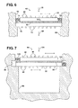
- FIG. 6 is a cross-sectional view of an optical switch using MEMS to shift the upper diffraction grating divider of the two inverted diffraction grating dividers relative to the lower diffraction grating divider wherein a liquid crystal layer serves as a fluid interface between the two diffraction grating dividers; and
- FIG. 7 is a diagrammatic illustration of a second application of the present invention in a switch for unpolarized sunlight in which the lateral movement or shift of the grating dividers in the double-sided grating assembly is accomplished by means of metals with known and calibrated coefficients of thermal expansion.
- Grating divider 12 comprises a substrate 16 of fused SiO 2 on which identical diffraction grating elements 18 , 20 , 22 made of TiO 2 are fused or mounted to the top surface of the substrate 16 in a regular periodic fashion so as to exhibit a period p of 540 nm, a height h of 175 nm and a width of 145 nm.
- the elements 18 , 20 , 22 are immersed in this case in air to create an air/TiO 2 interface.
- Other surrounding media, including solid substances, can also be used.
- the geometry is selected so as to produce a refraction angle in excess of the 43.6° critical angle of the TiO 2 air interface.
- the period p may be in the range of about 0.87 to about 0.93 ⁇ , where ⁇ is the wavelength of the incident light 24 , the fill factor r is in the range of about 0.22 to about 0.32 and h is in the range of about 0.24 to 0.34 ⁇ .
- the first order refraction components are diffracted by an angle of approximately 50°, well above the critical angle.
- the lower diffraction grating divider 14 comprises a substrate 26 of SiO 2 and periodically arranged TiO 2 grating elements 28 , 30 , 32 also immersed in air and having the exact same geometry as the grating elements 18 , 20 , 22 .
- grating divider 14 is identical to grating divider 12 but is inverted.
- light 24 may be thought as the input or incident light whereas light 34 is the output light which is transmitted through; i.e., the output light component when the transmittance or transmissivity 10 is operating at the “on” level hereinafter described.
- FIG. 2 is a graphical illustration of the degree of the transmittance of the 0 th order of the s-polarized incident light 24 when the diffraction grating elements 18 , 20 , 22 of the upper diffraction grating divider 12 are fully laterally aligned with the grating elements 28 , 30 , 32 of the lower diffraction grating divider 14 .
- the s-polarized light has the electric field in the y axis. Between about 550 nm and about 670 nm; i.e., in the “on” zone 36 , the transmittance is in excess of 95%.
- FIG. 3 the double-sided grating divider device 10 is shown in the “off” condition wherein the lower grating elements 28 , 30 , 32 are shifted by a distance d relative to the upper grating elements 18 , 20 , 22 wherein d is approximately p/4.
- FIG. 4 shows that the transmittance of the 0 th order component of normal incident unpolarized light in the wavelength range between about 550 and 650 nm is in the “off” zone 38 wherein the transmittance is near 0; i.e., less than about 5%.
- FIG. 5 there is shown a first practical application of the phenomenon of the present invention in an alignment marker for a SiO 2 multi-layer fabrication process.
- This device comprises an upper planar substrate 40 and, in spaced parallel relationship therewith a lower SiO 2 substrate 42 .
- the upper substrate 40 carries TiO 2 grating elements 44 , 46 , 48 , 50 in the four corners thereof arranged essentially in the fashion illustrated in FIGS. 1 and 3 .
- the lower SiO 2 substrate 42 carries diffraction grating elements 52 , 54 , 56 and a fourth diffraction grating divider in the upper left hand corner as viewed in FIG. 5 which is obscured by the drawing.
- the diffraction grating elements 48 , 52 are arranged to be essentially in alignment with one another when the substrates 40 , 42 are properly aligned but will be shifted relative to one another when the substrates are non-aligned along a lateral axis passing through and between the substrates 40 , 42 .
- Light 58 from a laser is directed normally toward the upper substrate 40 in such a way that when the grating elements are laterally aligned so as to exhibit the on condition represented by FIG. 2 , the 0 th order incident light component passes or is transmitted substantially fully through to a detector 60 to show the aligned condition. Conversely, when the substrates 40 , 42 are not aligned, indicating an alignment error in the fabrication process, substantially no light from the laser 58 reaches the detector and the fabrication process is thereafter terminated or paused to make suitable alignment adjustments. Similar alignment detection can be achieved for the orthogonal axis.
- an optical device in the form of an incident light valve or switch 62 comprising the combination of a planar upper SiO 2 substrate 64 carrying periodically arranged TiO 2 diffraction grating elements 66 and, in spaced parallel relationship thereto, a lower planar SiO 2 substrate with TiO 2 diffraction grating elements 72 .
- the lower substrate 70 is fixed in a frame 68 whereas the upper substrate 64 is sandwiched between microelectromechanical systems (MEMS) devices 74 , 76 so that the substrate 64 can be shifted relative to the lower substrate 70 to align and/or shift the diffraction grating elements 66 , 72 to act as a valve whereby the incident light 78 is switched between a low transmissivity condition wherein the output light 80 is essentially 0 and a high transmissivity wherein the output light component 80 is nearly 100%.
- MEMS microelectromechanical systems
- the lateral shifting of the substrates 64 , 70 is facilitated by means of a liquid crystal layer 82 which lies in the space between the inverted substrates 64 , 70 and has a refraction index of approximately 1.6. This layer can be replaced by an air layer with a refractive index of 1.
- the skylight 84 comprises an upper planar SiO 2 substrate 88 having periodically spaced diffraction grating elements 90 mounted to the upper surface thereof and exposed to incident sunlight 104 .
- the thermally responsive skylight 84 further comprises a lower planar SiO 2 substrate 92 having diffraction grating elements 94 regularly arranged thereon in the fashion described above with respect to FIGS. 1 and 3 .
- the two substrates 88 , 92 are separated by a liquid crystal layer 98 which is suitably contained and which acts as an optically transparent bearing between the two substrates 88 , 92 just as the layer 82 acts in the embodiment of FIG. 6 .
- a metal element having a known coefficient of thermal expansion which responds to temperature changes to cause a lateral shift in the position of the substrate 88 relative to the adjacent frame 96 .
- a second element 102 is mounted between the frame 96 and the right edge of the substrate 92 so as to cause a shift in the lateral shift in that substrate and the grating elements 94 in response to ambient temperature changes.
- the two shifts created by the metal elements 100 , 102 are cumulative and, when properly calibrated to achieve a shift of one-quarter of the period of the gratings 90 , 94 over the temperature range of interest, can produce a valving or switching function wherein the incident sunlight 104 is fully transmitted into the room 86 under low temperature conditions but is essentially fully blocked when ambient temperature becomes high.
- the embodiment of FIG. 7 can be used with additional sputter-deposited filters for selected wavelengths.
Landscapes
- Physics & Mathematics (AREA)
- General Physics & Mathematics (AREA)
- Optics & Photonics (AREA)
- Diffracting Gratings Or Hologram Optical Elements (AREA)
- Mechanical Light Control Or Optical Switches (AREA)
- Liquid Crystal (AREA)
Priority Applications (4)
| Application Number | Priority Date | Filing Date | Title |
|---|---|---|---|
| US12/692,688 US8072684B2 (en) | 2010-01-25 | 2010-01-25 | Optical device using laterally-shiftable diffraction gratings |
| JP2011011993A JP5647020B2 (ja) | 2010-01-25 | 2011-01-24 | 光学装置及び光バルブ |
| US13/079,339 US8976450B2 (en) | 2010-01-25 | 2011-04-04 | Optical light switch having two internally located diffraction gratings separated by liquid medium |
| US13/309,834 US9285519B2 (en) | 2010-01-25 | 2011-12-02 | Optical device using laterally-shiftable diffraction gratings |
Applications Claiming Priority (1)
| Application Number | Priority Date | Filing Date | Title |
|---|---|---|---|
| US12/692,688 US8072684B2 (en) | 2010-01-25 | 2010-01-25 | Optical device using laterally-shiftable diffraction gratings |
Related Child Applications (2)
| Application Number | Title | Priority Date | Filing Date |
|---|---|---|---|
| US13/079,339 Continuation-In-Part US8976450B2 (en) | 2010-01-25 | 2011-04-04 | Optical light switch having two internally located diffraction gratings separated by liquid medium |
| US13/309,834 Continuation US9285519B2 (en) | 2010-01-25 | 2011-12-02 | Optical device using laterally-shiftable diffraction gratings |
Publications (2)
| Publication Number | Publication Date |
|---|---|
| US20110181956A1 US20110181956A1 (en) | 2011-07-28 |
| US8072684B2 true US8072684B2 (en) | 2011-12-06 |
Family
ID=44308768
Family Applications (2)
| Application Number | Title | Priority Date | Filing Date |
|---|---|---|---|
| US12/692,688 Expired - Fee Related US8072684B2 (en) | 2010-01-25 | 2010-01-25 | Optical device using laterally-shiftable diffraction gratings |
| US13/309,834 Expired - Fee Related US9285519B2 (en) | 2010-01-25 | 2011-12-02 | Optical device using laterally-shiftable diffraction gratings |
Family Applications After (1)
| Application Number | Title | Priority Date | Filing Date |
|---|---|---|---|
| US13/309,834 Expired - Fee Related US9285519B2 (en) | 2010-01-25 | 2011-12-02 | Optical device using laterally-shiftable diffraction gratings |
Country Status (2)
| Country | Link |
|---|---|
| US (2) | US8072684B2 (ja) |
| JP (1) | JP5647020B2 (ja) |
Cited By (2)
| Publication number | Priority date | Publication date | Assignee | Title |
|---|---|---|---|---|
| US20110181957A1 (en) * | 2010-01-25 | 2011-07-28 | Toyota Motor Engineering And Manufacturing North America, Inc. | Optical light switch using double-sided diffraction structure |
| US20120075703A1 (en) * | 2010-01-25 | 2012-03-29 | The Trustees Of The University Of Pennsylvania | Optical device using laterally-shiftable diffraction gratings |
Families Citing this family (2)
| Publication number | Priority date | Publication date | Assignee | Title |
|---|---|---|---|---|
| US8675279B2 (en) * | 2009-12-15 | 2014-03-18 | Toyota Motor Engineering And Manufacturing North America, Inc. | Grating structure for dividing light |
| TWI675224B (zh) * | 2018-06-29 | 2019-10-21 | 揚明光學股份有限公司 | 成像位移模組及其製造方法 |
Citations (12)
| Publication number | Priority date | Publication date | Assignee | Title |
|---|---|---|---|---|
| US4331972A (en) * | 1978-11-09 | 1982-05-25 | Rajchman Jan A | Light valve, light valve display, and method |
| US4402610A (en) | 1979-12-18 | 1983-09-06 | Thomson-Csf | Optical system for the automatic alignment of two motifs comprising alignment marks of the grating type, particularly in direct photorepetition on silicon |
| US4729640A (en) * | 1984-10-03 | 1988-03-08 | Canon Kabushiki Kaisha | Liquid crystal light modulation device |
| US4781442A (en) | 1985-10-31 | 1988-11-01 | Commissariat A L'energie Atomique | Optoelectronic switch with a power threshold and its control process |
| US5434434A (en) | 1992-03-12 | 1995-07-18 | Nec Corporation | Semiconductor optical device having device regions and diffraction gratings |
| US5477351A (en) | 1992-04-10 | 1995-12-19 | Matsushita Electric Industrial Co., Ltd. | Polymer dispersed liquid crystal panel with diffraction grating and reflective counter electrode |
| US5915051A (en) | 1997-01-21 | 1999-06-22 | Massascusetts Institute Of Technology | Wavelength-selective optical add/drop switch |
| US6643424B2 (en) | 2001-08-31 | 2003-11-04 | International Business Machines Corporation | Silicon oxynitride optical waveguide switch with wavelength locked feedback control |
| US6858462B2 (en) | 2000-04-11 | 2005-02-22 | Gratings, Inc. | Enhanced light absorption of solar cells and photodetectors by diffraction |
| US6885789B2 (en) | 2002-06-07 | 2005-04-26 | Fujitsu Limited | Optical switch fabricated by a thin film process |
| US7187836B2 (en) | 2005-06-02 | 2007-03-06 | Heng-Sheng Kuo | Light-guiding module |
| US7263260B2 (en) | 2005-03-14 | 2007-08-28 | Matsushita Electric Industrial Co., Ltd. | Low cost, high precision multi-point optical component attachment |
Family Cites Families (22)
| Publication number | Priority date | Publication date | Assignee | Title |
|---|---|---|---|---|
| JPS6186724A (ja) * | 1984-10-04 | 1986-05-02 | Canon Inc | グレ−テイング型光制御素子 |
| JPH04151434A (ja) * | 1990-10-12 | 1992-05-25 | Takagi Ind Co Ltd | 給湯システム |
| US5430561A (en) | 1991-07-17 | 1995-07-04 | Fujitsu Limited | Optical space switch employing 2 parallel diffraction gratings and a polarization rotating element |
| JP3156684B2 (ja) | 1998-11-16 | 2001-04-16 | 日本電気株式会社 | 光スイッチ |
| US6721473B1 (en) | 2001-02-02 | 2004-04-13 | Cheetah Omni, Llc | Variable blazed grating based signal processing |
| US6868462B2 (en) * | 2001-09-12 | 2005-03-15 | Hewlett-Packard Development Company, L.P. | Intermediate resource management device |
| US6728023B1 (en) * | 2002-05-28 | 2004-04-27 | Silicon Light Machines | Optical device arrays with optimized image resolution |
| US6747773B2 (en) * | 2002-10-31 | 2004-06-08 | Agilent Technologies, Inc. | Method and structure for stub tunable resonant cavity for photonic crystals |
| NO318360B1 (no) * | 2002-12-30 | 2005-03-07 | Sinvent As | Konfigurerbart diffraktiv optisk element |
| CN101142505B (zh) | 2004-02-26 | 2010-05-05 | 斯欧普迪克尔股份有限公司 | 绝缘体上硅(soi)结构中的光的主动操控装置 |
| JP2005258053A (ja) * | 2004-03-11 | 2005-09-22 | Nippon Sheet Glass Co Ltd | 透過型回折格子 |
| US8018508B2 (en) * | 2004-04-13 | 2011-09-13 | Panasonic Corporation | Light-collecting device and solid-state imaging apparatus |
| US7173764B2 (en) * | 2004-04-22 | 2007-02-06 | Sandia Corporation | Apparatus comprising a tunable nanomechanical near-field grating and method for controlling far-field emission |
| JP4958041B2 (ja) * | 2007-01-19 | 2012-06-20 | 株式会社東芝 | 回折格子、光変調器及び表示装置 |
| JP2008224786A (ja) * | 2007-03-09 | 2008-09-25 | Ricoh Co Ltd | 光スイッチング素子とスイッチング素子と光スイッチング素子アレイと画像表示装置 |
| DE102007051520B4 (de) * | 2007-10-19 | 2021-01-14 | Seereal Technologies S.A. | Komplexwertiger räumlicher Lichtmodulator, räumliche Lichtmodulationseinrichtung und Verfahren zur Modulation eines Wellenfeldes |
| JP2009134232A (ja) * | 2007-11-09 | 2009-06-18 | Sony Corp | 可変回折格子、光量制御装置、光ピックアップ及び光ディスク装置 |
| US8675279B2 (en) * | 2009-12-15 | 2014-03-18 | Toyota Motor Engineering And Manufacturing North America, Inc. | Grating structure for dividing light |
| US8976450B2 (en) * | 2010-01-25 | 2015-03-10 | Toyota Motor Engineering & Manufacturing North America, Inc. | Optical light switch having two internally located diffraction gratings separated by liquid medium |
| US8072684B2 (en) * | 2010-01-25 | 2011-12-06 | Toyota Motor Engineering & Manufacturing North America, Inc. | Optical device using laterally-shiftable diffraction gratings |
| US9136406B2 (en) * | 2010-07-07 | 2015-09-15 | Toyota Motor Engineering & Manufacturing North America, Inc. | Solar cell assembly with diffraction gratings |
| US8687277B2 (en) * | 2010-08-11 | 2014-04-01 | Kenneth C. Johnson | Stacked-grating light modulator |
-
2010
- 2010-01-25 US US12/692,688 patent/US8072684B2/en not_active Expired - Fee Related
-
2011
- 2011-01-24 JP JP2011011993A patent/JP5647020B2/ja not_active Expired - Fee Related
- 2011-12-02 US US13/309,834 patent/US9285519B2/en not_active Expired - Fee Related
Patent Citations (12)
| Publication number | Priority date | Publication date | Assignee | Title |
|---|---|---|---|---|
| US4331972A (en) * | 1978-11-09 | 1982-05-25 | Rajchman Jan A | Light valve, light valve display, and method |
| US4402610A (en) | 1979-12-18 | 1983-09-06 | Thomson-Csf | Optical system for the automatic alignment of two motifs comprising alignment marks of the grating type, particularly in direct photorepetition on silicon |
| US4729640A (en) * | 1984-10-03 | 1988-03-08 | Canon Kabushiki Kaisha | Liquid crystal light modulation device |
| US4781442A (en) | 1985-10-31 | 1988-11-01 | Commissariat A L'energie Atomique | Optoelectronic switch with a power threshold and its control process |
| US5434434A (en) | 1992-03-12 | 1995-07-18 | Nec Corporation | Semiconductor optical device having device regions and diffraction gratings |
| US5477351A (en) | 1992-04-10 | 1995-12-19 | Matsushita Electric Industrial Co., Ltd. | Polymer dispersed liquid crystal panel with diffraction grating and reflective counter electrode |
| US5915051A (en) | 1997-01-21 | 1999-06-22 | Massascusetts Institute Of Technology | Wavelength-selective optical add/drop switch |
| US6858462B2 (en) | 2000-04-11 | 2005-02-22 | Gratings, Inc. | Enhanced light absorption of solar cells and photodetectors by diffraction |
| US6643424B2 (en) | 2001-08-31 | 2003-11-04 | International Business Machines Corporation | Silicon oxynitride optical waveguide switch with wavelength locked feedback control |
| US6885789B2 (en) | 2002-06-07 | 2005-04-26 | Fujitsu Limited | Optical switch fabricated by a thin film process |
| US7263260B2 (en) | 2005-03-14 | 2007-08-28 | Matsushita Electric Industrial Co., Ltd. | Low cost, high precision multi-point optical component attachment |
| US7187836B2 (en) | 2005-06-02 | 2007-03-06 | Heng-Sheng Kuo | Light-guiding module |
Non-Patent Citations (3)
| Title |
|---|
| Brundett, D. L., Glytsis, E. N., and Gaylord, T. K., "Normal Incidence Guided Mode Resonant Grating Filters: Design and Experimental Demonstration", Opt. Lett. 23, 700 (1998). |
| Perry, T. S., "Tomorrow's TV-the grating light valve", IEEE Spectrum 41, 38, (2004). |
| Perry, T. S., "Tomorrow's TV—the grating light valve", IEEE Spectrum 41, 38, (2004). |
Cited By (4)
| Publication number | Priority date | Publication date | Assignee | Title |
|---|---|---|---|---|
| US20110181957A1 (en) * | 2010-01-25 | 2011-07-28 | Toyota Motor Engineering And Manufacturing North America, Inc. | Optical light switch using double-sided diffraction structure |
| US20120075703A1 (en) * | 2010-01-25 | 2012-03-29 | The Trustees Of The University Of Pennsylvania | Optical device using laterally-shiftable diffraction gratings |
| US8976450B2 (en) * | 2010-01-25 | 2015-03-10 | Toyota Motor Engineering & Manufacturing North America, Inc. | Optical light switch having two internally located diffraction gratings separated by liquid medium |
| US9285519B2 (en) * | 2010-01-25 | 2016-03-15 | Toyota Motor Engineering & Manufacturing North America, Inc. | Optical device using laterally-shiftable diffraction gratings |
Also Published As
| Publication number | Publication date |
|---|---|
| JP2011154370A (ja) | 2011-08-11 |
| US20110181956A1 (en) | 2011-07-28 |
| US9285519B2 (en) | 2016-03-15 |
| US20120075703A1 (en) | 2012-03-29 |
| JP5647020B2 (ja) | 2014-12-24 |
Similar Documents
| Publication | Publication Date | Title |
|---|---|---|
| US9921371B2 (en) | Light guide element and image display device | |
| US9285519B2 (en) | Optical device using laterally-shiftable diffraction gratings | |
| JP4722831B2 (ja) | 液晶セルプラットホーム | |
| US7155073B2 (en) | Polarization element and optical device using polarization element | |
| EP2260349B1 (en) | Controllable light angle selector | |
| US20130175449A1 (en) | Infrared detector comprising a package integrating at least one diffraction grating | |
| KR20050007422A (ko) | 튜너블 광 파장 필터의 폐루프 제어 | |
| US8976450B2 (en) | Optical light switch having two internally located diffraction gratings separated by liquid medium | |
| JP2011070219A (ja) | 可視スペクトル用の埋込み型ワイヤ・グリッド偏光子 | |
| US7012747B2 (en) | Polarizing beam splitter and polarizer using the same | |
| Gao et al. | Controlling interface states in 1D photonic crystals by tuning bulk geometric phases | |
| JP4508048B2 (ja) | 液晶レンズおよび光ヘッド装置 | |
| JP4369256B2 (ja) | 分光光学素子 | |
| US20060072114A1 (en) | Apparatus and mehod for sensing with metal optical filters | |
| Lee et al. | Near-flat top bandpass filter based on non-local resonance in a dielectric metasurface | |
| Hsu et al. | Bulk-micromachined optical filter based on guided-mode resonance in silicon-nitride membrane | |
| US6914715B2 (en) | Optical element | |
| KR20100030486A (ko) | 파장 가변 필터 | |
| JP2011154370A5 (ja) | ||
| EP1540315A1 (en) | Optical waveguide interferometer comprising a laminate structure with a first planar waveguide monolayer and a second sandwich layer | |
| KR102452388B1 (ko) | 고분해능을 가지는 패브리-페로 필터 | |
| Ren et al. | Wide wavelength range tunable guided-mode resonance filter based on incident angle rotation | |
| EP1605286A1 (en) | Waveguide device using photonic crystal | |
| CN109581587A (zh) | 基于调谐液滴分布的可调谐布拉格波导光栅滤波器 | |
| Wu et al. | Terahertz membrane sensing based on terahertz composite slabs with enhanced fields |
Legal Events
| Date | Code | Title | Description |
|---|---|---|---|
| AS | Assignment |
Owner name: TRUSTEES OF THE UNIVERSITY OF PENNSYLVANIA, PENNSY Free format text: ASSIGNMENT OF ASSIGNORS INTEREST;ASSIGNOR:ENGHETA, NADER;REEL/FRAME:023988/0265 Effective date: 20100112 Owner name: TOYOTA MOTOR ENGINEERING & MANUFACTURING NORTH AME Free format text: ASSIGNMENT OF ASSIGNORS INTEREST;ASSIGNOR:IIZUKA, HIDEO;REEL/FRAME:023988/0205 Effective date: 20100112 |
|
| AS | Assignment |
Owner name: TOYOTA MOTOR ENGINEERING & MANUFACTURING NORTH AME Free format text: ASSIGNMENT OF ASSIGNORS INTEREST;ASSIGNOR:IIZUKA, HIDEO;REEL/FRAME:026179/0421 Effective date: 20110426 |
|
| STCF | Information on status: patent grant |
Free format text: PATENTED CASE |
|
| AS | Assignment |
Owner name: KABUSHIKI KAISHA TOYOTA CHUO KENKYUSHO, JAPAN Free format text: ASSIGNMENT OF ASSIGNORS INTEREST;ASSIGNOR:TOYOTA MOTOR ENGINEERING & MANUFACTURING NORTH AMERICA, INC.;REEL/FRAME:027474/0787 Effective date: 20111214 |
|
| FEPP | Fee payment procedure |
Free format text: PAYOR NUMBER ASSIGNED (ORIGINAL EVENT CODE: ASPN); ENTITY STATUS OF PATENT OWNER: LARGE ENTITY |
|
| FPAY | Fee payment |
Year of fee payment: 4 |
|
| FEPP | Fee payment procedure |
Free format text: MAINTENANCE FEE REMINDER MAILED (ORIGINAL EVENT CODE: REM.); ENTITY STATUS OF PATENT OWNER: LARGE ENTITY |
|
| LAPS | Lapse for failure to pay maintenance fees |
Free format text: PATENT EXPIRED FOR FAILURE TO PAY MAINTENANCE FEES (ORIGINAL EVENT CODE: EXP.); ENTITY STATUS OF PATENT OWNER: LARGE ENTITY |
|
| STCH | Information on status: patent discontinuation |
Free format text: PATENT EXPIRED DUE TO NONPAYMENT OF MAINTENANCE FEES UNDER 37 CFR 1.362 |
|
| FP | Lapsed due to failure to pay maintenance fee |
Effective date: 20191206 |