US8050367B2 - Receiving amplitude correction circuit, receiving amplitude correction method, and receiver using the same - Google Patents
Receiving amplitude correction circuit, receiving amplitude correction method, and receiver using the same Download PDFInfo
- Publication number
- US8050367B2 US8050367B2 US12/066,877 US6687706A US8050367B2 US 8050367 B2 US8050367 B2 US 8050367B2 US 6687706 A US6687706 A US 6687706A US 8050367 B2 US8050367 B2 US 8050367B2
- Authority
- US
- United States
- Prior art keywords
- unit
- band limitation
- digital signal
- multiplier
- amplitude
- Prior art date
- Legal status (The legal status is an assumption and is not a legal conclusion. Google has not performed a legal analysis and makes no representation as to the accuracy of the status listed.)
- Expired - Fee Related, expires
Links
- 238000012937 correction Methods 0.000 title claims description 47
- 238000000034 method Methods 0.000 title claims description 14
- 238000012545 processing Methods 0.000 claims abstract description 33
- 238000006243 chemical reaction Methods 0.000 claims description 15
- 238000004891 communication Methods 0.000 claims description 10
- 238000010586 diagram Methods 0.000 description 8
- 238000011144 upstream manufacturing Methods 0.000 description 2
- 230000005540 biological transmission Effects 0.000 description 1
- 238000013461 design Methods 0.000 description 1
- 238000005516 engineering process Methods 0.000 description 1
- 238000012546 transfer Methods 0.000 description 1
Images


Classifications
-
- H—ELECTRICITY
- H03—ELECTRONIC CIRCUITRY
- H03G—CONTROL OF AMPLIFICATION
- H03G3/00—Gain control in amplifiers or frequency changers
- H03G3/20—Automatic control
- H03G3/30—Automatic control in amplifiers having semiconductor devices
- H03G3/3089—Control of digital or coded signals
-
- H—ELECTRICITY
- H03—ELECTRONIC CIRCUITRY
- H03G—CONTROL OF AMPLIFICATION
- H03G3/00—Gain control in amplifiers or frequency changers
- H03G3/001—Digital control of analog signals
-
- H—ELECTRICITY
- H03—ELECTRONIC CIRCUITRY
- H03G—CONTROL OF AMPLIFICATION
- H03G3/00—Gain control in amplifiers or frequency changers
- H03G3/20—Automatic control
- H03G3/30—Automatic control in amplifiers having semiconductor devices
- H03G3/3052—Automatic control in amplifiers having semiconductor devices in bandpass amplifiers (H.F. or I.F.) or in frequency-changers used in a (super)heterodyne receiver
-
- H—ELECTRICITY
- H04—ELECTRIC COMMUNICATION TECHNIQUE
- H04B—TRANSMISSION
- H04B1/00—Details of transmission systems, not covered by a single one of groups H04B3/00 - H04B13/00; Details of transmission systems not characterised by the medium used for transmission
- H04B1/06—Receivers
- H04B1/16—Circuits
- H04B1/30—Circuits for homodyne or synchrodyne receivers
-
- H—ELECTRICITY
- H03—ELECTRONIC CIRCUITRY
- H03G—CONTROL OF AMPLIFICATION
- H03G2201/00—Indexing scheme relating to subclass H03G
- H03G2201/30—Gain control characterized by the type of controlled signal
- H03G2201/302—Gain control characterized by the type of controlled signal being baseband signal
Definitions
- Receivers in a wireless communication apparatus include a direct-conversion type receiver as shown in FIG. 1 .
- radio-frequency signals received by an antenna 201 are amplified by a low-noise amplifier (hereinafter abbreviated to “LNA”) 202 .
- LNA low-noise amplifier
- a duplexer, a radio-frequency filter (a broad-band filter that is not used to limit a channel band), and the like are provided between the antenna 201 and the LNA 202 . However, they are omitted from the drawings.
- the entire receiving band which is not a channel, is extracted from the signals amplified in the LNA 202 by a radio-frequency band-pass filter (hereinafter abbreviated to “RF BPF”) 203 , so that signals in bands other than the receiving band, such as a transmitting signal transmitted by the wireless communication apparatus itself, are suppressed.
- the output of the RF BPF 203 is inputted to a quadrature demodulator circuit 204 .
- the quadrature demodulator circuit 204 demodulates the input signal and outputs an I component that is an in-phase component and a Q component that is a quadrature component.
- FIG. 2 is a diagram showing the digital signal processing circuit 100 .
- a digital amplitude calculator 303 calculates an average amplitude of the signals, for example, within one slot in CDMA or TDMA from the digital I signal and Q signal transmitted from the base band circuit 207 shown in FIG. 1 .
- a subtractor 302 computes a difference between the calculation result of the average amplitude and a targeted reference amplitude.
- the computed difference is inputted into a digital gain control data generator 301 .
- the digital gain control data generator 301 generates gain control data for controlling gains of the VGAs from the computed difference.
- the signal levels of the I component and the Q component are automatically adjusted so that the levels of the input signals to the A/D converters 215 and 216 optimally fall within dynamic ranges of the A/D converters 215 and 216 (AGC).
- Patent Document 1 Japanese laid-open patent publication No. 2001-168664.
- EVM Error Vector Magnitude
- FIG. 3 An example in which the channel filters are formed by digital filters is shown in FIG. 3 .
- equivalent parts to those shown in FIG. 1 are denoted by the same reference numerals.
- FIG. 3 shows an example in which the channel filters 205 and 206 shown in FIG. 1 are respectively replaced with digital filters (DLPF) 217 and 218 , which are disposed on the downstream side of the A/D converters 215 and 216 .
- the channel filters for digital processing are formed by low-pass filters.
- those channel filters may be high-pass filters for removing a DC offset.
- low-pass filters for preventing aliasing caused by A/D conversion may be left on the upstream side of the A/D converters 215 and 216 .
- the aforementioned problems in the prior art are caused by the fact that input and output levels of the digital channel filter are not equal to each other or are not within a range of a predetermined level difference when there are a desired wave and an interference wave other than the desired wave. Therefore, the present invention adopts such arrangement that the input and output levels of the digital channel filter are made averagely substantially equal to each other or adjusted to have a predetermined level difference.
- an amplitude of a digital signal before an interference wave has been suppressed by a digital filter as a channel filter and an amplitude of a digital signal after the interference wave has been suppressed are made averagely substantially equal to each other or adjusted to have a predetermined difference.
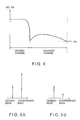
- FIG. 4 is a graph showing frequency characteristics of digital low-pass filters shown in FIG. 3 .
- FIG. 8 is a block diagram showing an arrangement of a receiver according to another embodiment of the present invention.
- an average amplitude Ain immediately before the channel filters 217 and 218 and an average amplitude Aout immediately after the channel filters 217 and 218 at a certain slot are defined by the following formulas (1) and (2).
- the average amplitudes calculated by the amplitude calculation circuits 101 and 102 are inputted to the gain difference calculation circuit 103 (multiplier computation unit).
- a multiplier a to be provided to the multiplier units 104 and 105 is computed in the gain difference calculation circuit 103 .
- the outputs of the channel filters 217 and 218 are multiplied by the multiplier ⁇ in the multiplier units 104 and 105 , respectively.
- Those multiplication results are introduced as a digital I signal and Q signal to the digital signal processing circuit ( FIG. 2 ).
- Other components are the same as shown in FIG. 3 .
- the amplitude calculation circuit 101 and 102 , the gain difference calculation circuit 103 , and the multiplier units 104 and 105 may collectively be referred to as a correction unit.
Landscapes
- Engineering & Computer Science (AREA)
- Computer Networks & Wireless Communication (AREA)
- Signal Processing (AREA)
- Circuits Of Receivers In General (AREA)
- Control Of Amplification And Gain Control (AREA)
Applications Claiming Priority (4)
| Application Number | Priority Date | Filing Date | Title |
|---|---|---|---|
| JP2005266179 | 2005-09-14 | ||
| JP2005266179 | 2005-09-14 | ||
| JP2005-266179 | 2005-09-14 | ||
| PCT/JP2006/318665 WO2007032550A1 (ja) | 2005-09-14 | 2006-09-14 | 受信振幅補正回路及び受信振幅補正方法並びにそれを用いた受信機 |
Publications (2)
| Publication Number | Publication Date |
|---|---|
| US20090285340A1 US20090285340A1 (en) | 2009-11-19 |
| US8050367B2 true US8050367B2 (en) | 2011-11-01 |
Family
ID=37865120
Family Applications (1)
| Application Number | Title | Priority Date | Filing Date |
|---|---|---|---|
| US12/066,877 Expired - Fee Related US8050367B2 (en) | 2005-09-14 | 2006-09-14 | Receiving amplitude correction circuit, receiving amplitude correction method, and receiver using the same |
Country Status (5)
| Country | Link |
|---|---|
| US (1) | US8050367B2 (zh) |
| EP (1) | EP1944871A4 (zh) |
| JP (1) | JP4737458B2 (zh) |
| CN (1) | CN101263659B (zh) |
| WO (1) | WO2007032550A1 (zh) |
Cited By (1)
| Publication number | Priority date | Publication date | Assignee | Title |
|---|---|---|---|---|
| US20120177368A1 (en) * | 2011-01-07 | 2012-07-12 | Fujitsu Limited | Optical transmission apparatus and analog-to-digital conversion apparatus |
Families Citing this family (3)
| Publication number | Priority date | Publication date | Assignee | Title |
|---|---|---|---|---|
| CN101291517B (zh) * | 2007-04-17 | 2012-01-04 | 华为技术有限公司 | 一种测量处理方法及装置 |
| JP2009088972A (ja) * | 2007-09-28 | 2009-04-23 | Toshiba Corp | 無線通信の受信装置 |
| JP5783251B2 (ja) * | 2011-07-08 | 2015-09-24 | 日本電気株式会社 | 受信装置及び受信方法 |
Citations (14)
| Publication number | Priority date | Publication date | Assignee | Title |
|---|---|---|---|---|
| US5467399A (en) * | 1992-12-14 | 1995-11-14 | Ford Motor Company | Coherent signal generation in digital radio receiver |
| JP2000252868A (ja) | 1999-03-01 | 2000-09-14 | Toshiba Corp | Cdma通信装置とその自動利得制御回路 |
| JP2001168664A (ja) | 1999-12-08 | 2001-06-22 | Nec Corp | 受信電力計算回路及びそれを用いた受信機 |
| US20020102941A1 (en) * | 2001-01-31 | 2002-08-01 | Nokia Mobile Phones Ltd. | Measurement method and device for activating interfrequency handover in a wireless telecommunication network |
| US20020163979A1 (en) * | 2001-05-01 | 2002-11-07 | Tantivy Communictions, Inc. | Narrowband gain control of receiver with digital post filtering |
| US20020181568A1 (en) | 2001-06-01 | 2002-12-05 | Prater James S. | Over-sampling A/D converter with adjacent channel power detection |
| US20030064695A1 (en) * | 2001-09-28 | 2003-04-03 | Hong Shi | LNA gain adjustment in an RF receiver to compensate for intermodulation interference |
| EP1326347A2 (en) | 2001-12-28 | 2003-07-09 | Nokia Corporation | Method and apparatus for scaling the dynamic range of a receiver |
| US20040097212A1 (en) * | 2002-01-29 | 2004-05-20 | Hidenori Matsumoto | Direct conversion receiver and dc offset reducing method |
| JP2004153718A (ja) | 2002-10-31 | 2004-05-27 | Samsung Yokohama Research Institute Co Ltd | Agc制御回路及びagc増幅器制御方法 |
| WO2004068754A1 (ja) | 2003-01-30 | 2004-08-12 | Fujitsu Limited | マルチキャリア受信装置 |
| US20060017602A1 (en) * | 2004-07-22 | 2006-01-26 | Infineon Technologies Ag. | Mobile radio receiver with hybrid gain setting and method for gain setting |
| US7809047B2 (en) * | 2001-11-12 | 2010-10-05 | Andrew Llc | Digital repeater having bandpass filtering, adaptive pre-equalization and suppression of natural oscillation |
| US7907589B2 (en) * | 2003-12-01 | 2011-03-15 | Panasonic Corporation | Reception apparatus and reception method |
Family Cites Families (2)
| Publication number | Priority date | Publication date | Assignee | Title |
|---|---|---|---|---|
| JP2001086183A (ja) * | 1999-09-09 | 2001-03-30 | Alps Electric Co Ltd | デジタル変調信号受信機 |
| CN2580690Y (zh) * | 2002-11-22 | 2003-10-15 | 乔巍巍 | 通信接收机低频降噪电路装置 |
-
2006
- 2006-09-14 WO PCT/JP2006/318665 patent/WO2007032550A1/ja active Application Filing
- 2006-09-14 CN CN2006800339480A patent/CN101263659B/zh not_active Expired - Fee Related
- 2006-09-14 EP EP06810353A patent/EP1944871A4/en not_active Withdrawn
- 2006-09-14 US US12/066,877 patent/US8050367B2/en not_active Expired - Fee Related
- 2006-09-14 JP JP2007535583A patent/JP4737458B2/ja not_active Expired - Fee Related
Patent Citations (14)
| Publication number | Priority date | Publication date | Assignee | Title |
|---|---|---|---|---|
| US5467399A (en) * | 1992-12-14 | 1995-11-14 | Ford Motor Company | Coherent signal generation in digital radio receiver |
| JP2000252868A (ja) | 1999-03-01 | 2000-09-14 | Toshiba Corp | Cdma通信装置とその自動利得制御回路 |
| JP2001168664A (ja) | 1999-12-08 | 2001-06-22 | Nec Corp | 受信電力計算回路及びそれを用いた受信機 |
| US20020102941A1 (en) * | 2001-01-31 | 2002-08-01 | Nokia Mobile Phones Ltd. | Measurement method and device for activating interfrequency handover in a wireless telecommunication network |
| US20020163979A1 (en) * | 2001-05-01 | 2002-11-07 | Tantivy Communictions, Inc. | Narrowband gain control of receiver with digital post filtering |
| US20020181568A1 (en) | 2001-06-01 | 2002-12-05 | Prater James S. | Over-sampling A/D converter with adjacent channel power detection |
| US20030064695A1 (en) * | 2001-09-28 | 2003-04-03 | Hong Shi | LNA gain adjustment in an RF receiver to compensate for intermodulation interference |
| US7809047B2 (en) * | 2001-11-12 | 2010-10-05 | Andrew Llc | Digital repeater having bandpass filtering, adaptive pre-equalization and suppression of natural oscillation |
| EP1326347A2 (en) | 2001-12-28 | 2003-07-09 | Nokia Corporation | Method and apparatus for scaling the dynamic range of a receiver |
| US20040097212A1 (en) * | 2002-01-29 | 2004-05-20 | Hidenori Matsumoto | Direct conversion receiver and dc offset reducing method |
| JP2004153718A (ja) | 2002-10-31 | 2004-05-27 | Samsung Yokohama Research Institute Co Ltd | Agc制御回路及びagc増幅器制御方法 |
| WO2004068754A1 (ja) | 2003-01-30 | 2004-08-12 | Fujitsu Limited | マルチキャリア受信装置 |
| US7907589B2 (en) * | 2003-12-01 | 2011-03-15 | Panasonic Corporation | Reception apparatus and reception method |
| US20060017602A1 (en) * | 2004-07-22 | 2006-01-26 | Infineon Technologies Ag. | Mobile radio receiver with hybrid gain setting and method for gain setting |
Cited By (2)
| Publication number | Priority date | Publication date | Assignee | Title |
|---|---|---|---|---|
| US20120177368A1 (en) * | 2011-01-07 | 2012-07-12 | Fujitsu Limited | Optical transmission apparatus and analog-to-digital conversion apparatus |
| US9363022B2 (en) * | 2011-01-07 | 2016-06-07 | Fujitsu Limited | Optical transmission apparatus and analog-to-digital conversion apparatus |
Also Published As
| Publication number | Publication date |
|---|---|
| WO2007032550A1 (ja) | 2007-03-22 |
| US20090285340A1 (en) | 2009-11-19 |
| CN101263659B (zh) | 2012-08-08 |
| EP1944871A4 (en) | 2011-01-05 |
| CN101263659A (zh) | 2008-09-10 |
| JP4737458B2 (ja) | 2011-08-03 |
| JPWO2007032550A1 (ja) | 2009-03-19 |
| EP1944871A1 (en) | 2008-07-16 |
Similar Documents
| Publication | Publication Date | Title |
|---|---|---|
| US6044253A (en) | Method and apparatus using first and second variable gain control circuits to reduce cross modulation in a radio receiver | |
| US20140086370A1 (en) | Circuits, systems, and methods for managing automatic gain control in quadrature signal paths of a receiver | |
| WO2013008747A1 (ja) | 受信装置及び利得制御方法 | |
| US7986930B2 (en) | IQ imbalance image suppression in presence of unknown phase shift | |
| JPH09199961A (ja) | Agc装置 | |
| US6775336B1 (en) | Receiver and gain control method of the same | |
| US8050367B2 (en) | Receiving amplitude correction circuit, receiving amplitude correction method, and receiver using the same | |
| JP2004147000A (ja) | Agcシステム | |
| JP2001268145A (ja) | 振幅偏差補正回路 | |
| US8055232B2 (en) | Radio frequency receiving apparatus, radio frequency receiving method, LSI for radio frequency signal and LSI for base band signal | |
| US7805121B2 (en) | Radio signal receiver and gain control method thereof | |
| US6947472B2 (en) | Noise gain control | |
| JP4288458B2 (ja) | 振幅制限回路及びcdma通信装置 | |
| US20110274223A1 (en) | Agc tuner for mimo systems | |
| JP4554505B2 (ja) | デジタル信号受信装置 | |
| JP4843397B2 (ja) | 受信装置 | |
| US7447283B2 (en) | Method for automatic gain control, for instance in a telecommunication system, device and computer program product therefor | |
| JP2007081761A (ja) | 受信電界強度検出回路及びその方法並びにそれを用いた受信機 | |
| JP6947055B2 (ja) | 無線装置 | |
| JPH10173626A (ja) | 直接拡散cdma伝送方式の受信装置 | |
| JP2004242137A (ja) | 無線受信機 | |
| JP2004274453A (ja) | 無線基地局受信装置 | |
| KR100451171B1 (ko) | 씨디엠에이 수신부의 수신 데이터 처리 장치 | |
| JP2008011376A (ja) | 受信装置及びその利得制御方法 | |
| JP2008245006A (ja) | 受信機、及び集積回路 |
Legal Events
| Date | Code | Title | Description |
|---|---|---|---|
| AS | Assignment |
Owner name: NEC CORPORATION, TEXAS Free format text: ASSIGNMENT OF ASSIGNORS INTEREST;ASSIGNOR:ICHIHARA, MASAKI;REEL/FRAME:020651/0519 Effective date: 20080204 |
|
| AS | Assignment |
Owner name: LENOVO INNOVATIONS LIMITED (HONG KONG), HONG KONG Free format text: ASSIGNMENT OF ASSIGNORS INTEREST;ASSIGNOR:NEC CORPORATION;REEL/FRAME:033720/0767 Effective date: 20140618 |
|
| REMI | Maintenance fee reminder mailed | ||
| LAPS | Lapse for failure to pay maintenance fees | ||
| STCH | Information on status: patent discontinuation |
Free format text: PATENT EXPIRED DUE TO NONPAYMENT OF MAINTENANCE FEES UNDER 37 CFR 1.362 |
|
| FP | Lapsed due to failure to pay maintenance fee |
Effective date: 20151101 |