US7902003B2 - Semiconductor device and method for manufacturing the same - Google Patents
Semiconductor device and method for manufacturing the same Download PDFInfo
- Publication number
- US7902003B2 US7902003B2 US11/620,154 US62015407A US7902003B2 US 7902003 B2 US7902003 B2 US 7902003B2 US 62015407 A US62015407 A US 62015407A US 7902003 B2 US7902003 B2 US 7902003B2
- Authority
- US
- United States
- Prior art keywords
- nitrogen
- display device
- image display
- semiconductor layer
- manufacturing
- Prior art date
- Legal status (The legal status is an assumption and is not a legal conclusion. Google has not performed a legal analysis and makes no representation as to the accuracy of the status listed.)
- Expired - Fee Related, expires
Links
- 238000000034 method Methods 0.000 title claims abstract description 86
- 239000004065 semiconductor Substances 0.000 title claims abstract description 69
- 238000004519 manufacturing process Methods 0.000 title claims description 35
- 239000012535 impurity Substances 0.000 claims abstract description 47
- IJGRMHOSHXDMSA-UHFFFAOYSA-N Atomic nitrogen Chemical compound N#N IJGRMHOSHXDMSA-UHFFFAOYSA-N 0.000 claims abstract description 41
- 229910052757 nitrogen Inorganic materials 0.000 claims abstract description 40
- 238000002425 crystallisation Methods 0.000 claims abstract description 34
- 230000008025 crystallization Effects 0.000 claims abstract description 34
- 238000005224 laser annealing Methods 0.000 claims abstract description 30
- 229910052799 carbon Inorganic materials 0.000 claims abstract description 24
- 238000000137 annealing Methods 0.000 claims abstract description 16
- 239000002019 doping agent Substances 0.000 claims abstract description 15
- 150000002500 ions Chemical class 0.000 claims abstract description 9
- 230000004913 activation Effects 0.000 claims abstract description 7
- 229910052760 oxygen Inorganic materials 0.000 claims abstract description 6
- OKTJSMMVPCPJKN-UHFFFAOYSA-N Carbon Chemical compound [C] OKTJSMMVPCPJKN-UHFFFAOYSA-N 0.000 claims abstract description 5
- QVGXLLKOCUKJST-UHFFFAOYSA-N atomic oxygen Chemical compound [O] QVGXLLKOCUKJST-UHFFFAOYSA-N 0.000 claims abstract description 5
- 239000001301 oxygen Substances 0.000 claims abstract description 5
- 239000010408 film Substances 0.000 claims description 117
- 239000000758 substrate Substances 0.000 claims description 38
- 239000013078 crystal Substances 0.000 claims description 30
- 229910052710 silicon Inorganic materials 0.000 claims description 15
- 239000010703 silicon Substances 0.000 claims description 15
- 239000010409 thin film Substances 0.000 claims description 11
- 230000008018 melting Effects 0.000 claims description 5
- 238000002844 melting Methods 0.000 claims description 5
- 238000001953 recrystallisation Methods 0.000 claims description 4
- 230000001105 regulatory effect Effects 0.000 claims description 2
- -1 nitrogen ions Chemical class 0.000 claims 3
- 229910021420 polycrystalline silicon Inorganic materials 0.000 abstract description 44
- 229920005591 polysilicon Polymers 0.000 abstract description 44
- 229910021417 amorphous silicon Inorganic materials 0.000 abstract description 22
- 238000005499 laser crystallization Methods 0.000 abstract description 10
- 239000000356 contaminant Substances 0.000 abstract description 6
- 239000012686 silicon precursor Substances 0.000 abstract description 3
- 239000004973 liquid crystal related substance Substances 0.000 description 34
- 239000010410 layer Substances 0.000 description 31
- 239000002243 precursor Substances 0.000 description 19
- 230000000694 effects Effects 0.000 description 14
- 239000011521 glass Substances 0.000 description 14
- 230000015572 biosynthetic process Effects 0.000 description 11
- 238000000206 photolithography Methods 0.000 description 10
- 229910052581 Si3N4 Inorganic materials 0.000 description 9
- 230000003247 decreasing effect Effects 0.000 description 9
- 238000002513 implantation Methods 0.000 description 9
- 230000001681 protective effect Effects 0.000 description 9
- HQVNEWCFYHHQES-UHFFFAOYSA-N silicon nitride Chemical compound N12[Si]34N5[Si]62N3[Si]51N64 HQVNEWCFYHHQES-UHFFFAOYSA-N 0.000 description 9
- VYPSYNLAJGMNEJ-UHFFFAOYSA-N Silicium dioxide Chemical compound O=[Si]=O VYPSYNLAJGMNEJ-UHFFFAOYSA-N 0.000 description 8
- XUIMIQQOPSSXEZ-UHFFFAOYSA-N Silicon Chemical compound [Si] XUIMIQQOPSSXEZ-UHFFFAOYSA-N 0.000 description 8
- 229910052814 silicon oxide Inorganic materials 0.000 description 8
- 239000012212 insulator Substances 0.000 description 7
- 239000011159 matrix material Substances 0.000 description 7
- 239000013074 reference sample Substances 0.000 description 7
- 239000000523 sample Substances 0.000 description 7
- 238000005268 plasma chemical vapour deposition Methods 0.000 description 6
- 238000005229 chemical vapour deposition Methods 0.000 description 5
- 238000002474 experimental method Methods 0.000 description 5
- 229910052796 boron Inorganic materials 0.000 description 4
- 238000011109 contamination Methods 0.000 description 4
- 230000002093 peripheral effect Effects 0.000 description 4
- 229910052698 phosphorus Inorganic materials 0.000 description 4
- 230000002829 reductive effect Effects 0.000 description 4
- 238000009825 accumulation Methods 0.000 description 3
- 238000005530 etching Methods 0.000 description 3
- 239000007789 gas Substances 0.000 description 3
- 239000011229 interlayer Substances 0.000 description 3
- 230000001678 irradiating effect Effects 0.000 description 3
- 229910052751 metal Inorganic materials 0.000 description 3
- 239000002184 metal Substances 0.000 description 3
- LIVNPJMFVYWSIS-UHFFFAOYSA-N silicon monoxide Chemical compound [Si-]#[O+] LIVNPJMFVYWSIS-UHFFFAOYSA-N 0.000 description 3
- 239000007787 solid Substances 0.000 description 3
- 238000004544 sputter deposition Methods 0.000 description 3
- ZOXJGFHDIHLPTG-UHFFFAOYSA-N Boron Chemical compound [B] ZOXJGFHDIHLPTG-UHFFFAOYSA-N 0.000 description 2
- UFHFLCQGNIYNRP-UHFFFAOYSA-N Hydrogen Chemical compound [H][H] UFHFLCQGNIYNRP-UHFFFAOYSA-N 0.000 description 2
- OAICVXFJPJFONN-UHFFFAOYSA-N Phosphorus Chemical compound [P] OAICVXFJPJFONN-UHFFFAOYSA-N 0.000 description 2
- 229910052782 aluminium Inorganic materials 0.000 description 2
- XAGFODPZIPBFFR-UHFFFAOYSA-N aluminium Chemical compound [Al] XAGFODPZIPBFFR-UHFFFAOYSA-N 0.000 description 2
- 238000005520 cutting process Methods 0.000 description 2
- 238000000151 deposition Methods 0.000 description 2
- 238000005516 engineering process Methods 0.000 description 2
- 239000001257 hydrogen Substances 0.000 description 2
- 229910052739 hydrogen Inorganic materials 0.000 description 2
- 238000010348 incorporation Methods 0.000 description 2
- 239000011810 insulating material Substances 0.000 description 2
- 238000005468 ion implantation Methods 0.000 description 2
- 230000000873 masking effect Effects 0.000 description 2
- MGRWKWACZDFZJT-UHFFFAOYSA-N molybdenum tungsten Chemical compound [Mo].[W] MGRWKWACZDFZJT-UHFFFAOYSA-N 0.000 description 2
- 239000011574 phosphorus Substances 0.000 description 2
- 238000012545 processing Methods 0.000 description 2
- 238000011084 recovery Methods 0.000 description 2
- 239000000565 sealant Substances 0.000 description 2
- 238000007789 sealing Methods 0.000 description 2
- 238000000926 separation method Methods 0.000 description 2
- 239000002210 silicon-based material Substances 0.000 description 2
- 230000003746 surface roughness Effects 0.000 description 2
- 230000008961 swelling Effects 0.000 description 2
- 238000010521 absorption reaction Methods 0.000 description 1
- 230000002411 adverse Effects 0.000 description 1
- 238000004458 analytical method Methods 0.000 description 1
- 239000000969 carrier Substances 0.000 description 1
- 238000006243 chemical reaction Methods 0.000 description 1
- 150000001875 compounds Chemical class 0.000 description 1
- 239000000470 constituent Substances 0.000 description 1
- 230000008021 deposition Effects 0.000 description 1
- 238000013461 design Methods 0.000 description 1
- 238000011161 development Methods 0.000 description 1
- 238000009826 distribution Methods 0.000 description 1
- 238000001312 dry etching Methods 0.000 description 1
- 238000001035 drying Methods 0.000 description 1
- 230000005684 electric field Effects 0.000 description 1
- 230000005669 field effect Effects 0.000 description 1
- 230000005525 hole transport Effects 0.000 description 1
- 239000007943 implant Substances 0.000 description 1
- 238000002347 injection Methods 0.000 description 1
- 239000007924 injection Substances 0.000 description 1
- 230000000670 limiting effect Effects 0.000 description 1
- 230000010355 oscillation Effects 0.000 description 1
- 230000035515 penetration Effects 0.000 description 1
- 229920002120 photoresistant polymer Polymers 0.000 description 1
- 229920001690 polydopamine Polymers 0.000 description 1
- 238000007639 printing Methods 0.000 description 1
- 230000005855 radiation Effects 0.000 description 1
- 230000003685 thermal hair damage Effects 0.000 description 1
Images


Classifications
-
- H—ELECTRICITY
- H01—ELECTRIC ELEMENTS
- H01L—SEMICONDUCTOR DEVICES NOT COVERED BY CLASS H10
- H01L27/00—Devices consisting of a plurality of semiconductor or other solid-state components formed in or on a common substrate
- H01L27/02—Devices consisting of a plurality of semiconductor or other solid-state components formed in or on a common substrate including semiconductor components specially adapted for rectifying, oscillating, amplifying or switching and having potential barriers; including integrated passive circuit elements having potential barriers
- H01L27/12—Devices consisting of a plurality of semiconductor or other solid-state components formed in or on a common substrate including semiconductor components specially adapted for rectifying, oscillating, amplifying or switching and having potential barriers; including integrated passive circuit elements having potential barriers the substrate being other than a semiconductor body, e.g. an insulating body
- H01L27/1214—Devices consisting of a plurality of semiconductor or other solid-state components formed in or on a common substrate including semiconductor components specially adapted for rectifying, oscillating, amplifying or switching and having potential barriers; including integrated passive circuit elements having potential barriers the substrate being other than a semiconductor body, e.g. an insulating body comprising a plurality of TFTs formed on a non-semiconducting substrate, e.g. driving circuits for AMLCDs
- H01L27/1259—Multistep manufacturing methods
- H01L27/127—Multistep manufacturing methods with a particular formation, treatment or patterning of the active layer specially adapted to the circuit arrangement
- H01L27/1274—Multistep manufacturing methods with a particular formation, treatment or patterning of the active layer specially adapted to the circuit arrangement using crystallisation of amorphous semiconductor or recrystallisation of crystalline semiconductor
- H01L27/1285—Multistep manufacturing methods with a particular formation, treatment or patterning of the active layer specially adapted to the circuit arrangement using crystallisation of amorphous semiconductor or recrystallisation of crystalline semiconductor using control of the annealing or irradiation parameters, e.g. using different scanning direction or intensity for different transistors
-
- H—ELECTRICITY
- H01—ELECTRIC ELEMENTS
- H01L—SEMICONDUCTOR DEVICES NOT COVERED BY CLASS H10
- H01L21/00—Processes or apparatus adapted for the manufacture or treatment of semiconductor or solid state devices or of parts thereof
- H01L21/02—Manufacture or treatment of semiconductor devices or of parts thereof
- H01L21/02104—Forming layers
- H01L21/02365—Forming inorganic semiconducting materials on a substrate
- H01L21/02518—Deposited layers
- H01L21/02521—Materials
- H01L21/02524—Group 14 semiconducting materials
- H01L21/02532—Silicon, silicon germanium, germanium
-
- H—ELECTRICITY
- H01—ELECTRIC ELEMENTS
- H01L—SEMICONDUCTOR DEVICES NOT COVERED BY CLASS H10
- H01L21/00—Processes or apparatus adapted for the manufacture or treatment of semiconductor or solid state devices or of parts thereof
- H01L21/02—Manufacture or treatment of semiconductor devices or of parts thereof
- H01L21/02104—Forming layers
- H01L21/02365—Forming inorganic semiconducting materials on a substrate
- H01L21/02656—Special treatments
- H01L21/02664—Aftertreatments
- H01L21/02667—Crystallisation or recrystallisation of non-monocrystalline semiconductor materials, e.g. regrowth
- H01L21/02675—Crystallisation or recrystallisation of non-monocrystalline semiconductor materials, e.g. regrowth using laser beams
- H01L21/02683—Continuous wave laser beam
-
- H—ELECTRICITY
- H01—ELECTRIC ELEMENTS
- H01L—SEMICONDUCTOR DEVICES NOT COVERED BY CLASS H10
- H01L21/00—Processes or apparatus adapted for the manufacture or treatment of semiconductor or solid state devices or of parts thereof
- H01L21/02—Manufacture or treatment of semiconductor devices or of parts thereof
- H01L21/02104—Forming layers
- H01L21/02365—Forming inorganic semiconducting materials on a substrate
- H01L21/02656—Special treatments
- H01L21/02664—Aftertreatments
- H01L21/02667—Crystallisation or recrystallisation of non-monocrystalline semiconductor materials, e.g. regrowth
- H01L21/02691—Scanning of a beam
Definitions
- the present invention relates to a method for manufacturing an image display device using liquid crystal elements and organic light-emitting elements, particularly, an image display device incorporating drive circuits formed by low temperature polysilicon technology, and relates to an image display device produced by this manufacturing method.
- An image display device (hereinafter referred to as a display) using liquid crystal elements, namely, a liquid crystal display is widely used for a monitor of various kinds of information equipment such as television receivers and personal computers, owing to its features of a thin structure and low power consumption.
- the liquid crystal display for late mobile appliances is required to achieve higher image quality and higher resolution as well as to have added values such as improved functionality, a thinner and lighter structure, and reduced manufacturing cost.
- a system-in-display that incorporates drivers (drive circuits) for driving timing controllers and pixels, wherein the drivers are constructed with thin-film transistors (hereinafter also referred to as TFTs) using a low temperature polysilicon film on a glass substrate that is the same as for the liquid crystal display.
- driver circuits driver circuits
- TFTs thin-film transistors
- TFTs are already used to drive pixels in the liquid crystal display.
- an amorphous silicon material with low carrier mobility hereinafter simply referred to as mobility
- mobility amorphous silicon material with low carrier mobility
- an excimer laser annealing (ELA) process is a mainstream.
- the ELA process irradiates an amorphous silicon film with high-output excimer laser pulses, thereby melting and re-crystallizing a large area of silicon film. Since this ELA process does not control the crystal growing direction, the orientation of crystal grain boundaries is random and the grain size is small in the order of 0.2 to 0.8 ⁇ m. The thus formed crystal grains have a large surface roughness with the swelling grain boundaries.
- a technique of crystallizing polysilicon more like a single crystal is considered.
- a Selectively Enlarging Laser Crystallization (SELAX) process is disclosed in a compilation of papers submitted to the Society for Information Display 2002 International Symposium (Boston, 2002) PP158-161. This method is to move (scan) the laser radiation on the silicon film formed on the substrate (or the stage on which the substrate underlying the formed silicon film is loaded) in a certain direction with regard to the substrate surface, using continuous-wave (CW) laser or pseudo CW laser light with a extremely high pulse frequency of several tens of MHz or higher.
- CW continuous-wave
- the crystal grows along the certain direction.
- the crystal grain boundaries are formed substantially in parallel with the crystal growing direction. Consequently, no swelling takes place at the grain boundaries and, therefore, a film with a planar surface is obtained.
- the crystal grains are grown in a zone which is about 0.2-0.8 ⁇ m wide and about 2-8 ⁇ m long. This formation of the crystal grains introduces anisotropy between electrical conductivity in the crystal growing direction and that in the direction perpendicular to the growing direction. That is, the electrical conductivity in the crystal growing direction produces higher mobility, because of a decrease in the density of the crystal grain boundaries across which carriers pass.
- the CW laser light for example, a light obtained by converting a fixed laser wavelength of 1064 nm into 532 nm is used.
- the output of the CW laser light or the pseudo CW laser light is smaller than the pulse excimer laser. Therefore, the laser light must be shaped into a beam for efficient crystallization. That is, the shape of the beam irradiating the substrate should be a long and thin rectangle with its long axis perpendicular to the laser scan direction. This is intended to increase throughput by enlarging a region to be scanned at a time. The long side of this rectangle is, in most cases, not more than 100 ⁇ m, though depending on the laser output. Thus, crystallization by annealing using the CW laser is selectively applied only to peripheral circuit portions where high-performance TFTs are needed.
- a problem that is common for crystallization methods by annealing including, but not limited to, the ELA process, CW laser annealing, or other methods is impurity incorporation.
- carbon (C), nitrogen (N), and oxygen (O) impurities which are contamination sources exist in an undercoat layer (dielectric undercoat layer) and a precursor semiconductor film itself, and also in the atmosphere for crystallization. Therefore, the incorporation of these impurities is inevitable during the crystallization process.
- a 140-nm thick silicon nitride (SiN) film and a 100-nm thick silicon oxide (SiO) film are formed as the dielectric undercoat layer.
- a 50-nm thick amorphous silicon film was subsequently formed by a plasma chemical vapor deposition (CVD) process.
- CVD plasma chemical vapor deposition
- hydrogen in the amorphous silicon was reduced by annealing at 400° C.
- C, N, and O were implanted at concentrations from 1 ⁇ 10 18 cm ⁇ 3 to 2 ⁇ 10 20 cm ⁇ 3 to contaminate the amorphous silicon precursor semiconductor film on purpose.
- FIG. 1 represents relationships between the mobility as the result of TFT performance measured at a drain voltage of 0.1 V and the concentrations of the ion-implanted impurities.
- the concentrations of the C, N, and O impurities are plotted on the abscissa and the field effect mobility of TFT is plotted on the ordinate.
- a reference sample which is not implanted any impurity is marked with X.
- FIG. 1 shows a decrease in the mobility by contaminating the precursor semiconductor film with any of C, N, and O. Particularly, a significant decrease in the mobility occurs with the C contaminated sample and a decrease of 20% or more as compared with the reference sample was seen. To investigate a cause of this, mass analysis of the impurities in the crystallized polysilicon was carried out.
- FIGS. 2A through 2D represent the profiles of the concentrations of the impurities (C, N, and O) in regard to a precursor semiconductor and its crystallized polysilicon.
- FIGS. 2A , 2 B, 2 C, and 2 D show the impurity concentration profiles in a depth direction in the samples implanted with C, N, and O, respectively, by 1 ⁇ 10 20 cm ⁇ 3 , and in the reference sample not implanted with any impurity before and after crystallization.
- the results shown in FIG. 2 are those obtained by CW laser crystallization.
- the C contamination in the laser annealed silicon is mainly due to the incursion of C from the surface, when melt in the crystallization process. Since the impurity concentration is high at the surface or interface, the representative concentrations of the samples are those taken at the lowest concentration portion in the film.
- the concentration profiles of these impurities in the depth direction indicate a tendency that the concentration inside the film is low and the concentration at the surface and interface is high.
- the N and O implanted into the respective samples are expelled and their concentrations decrease from the initial concentrations.
- the N and O concentrations increase due to the incursion of N and O during the crystallization process.
- the N and O concentrations were initially 1.5 ⁇ 10 17 cm ⁇ 3 and 1 ⁇ 10 1 cm ⁇ 3 , respectively, and the concentrations increased to 2.5 ⁇ 10 17 cm ⁇ 3 and 8 ⁇ 10 18 cm ⁇ 3 . These values do not significantly differ from the N and O concentrations taken after crystallization in the samples implanted with N and O.
- N and O unlike C, the incursion of the surface contaminants and the constituent elements of the dielectric undercoat and the expelling thereof take place at the same time, resulting in the N and O concentrations in the film after crystallization falling in a given range. This is considered as the reason why the mobility decrease induced by N and O is smaller than that induced by C. This effect of expelling N and O is considered to take place because the solid solubility limits of N and O in silicon are low.
- amorphous silicon is annealed by laser for silicon crystallization, then P or B ions are implanted into the source and drain regions, and activation annealing is performed.
- P or B ions are implanted into the source and drain regions, and activation annealing is performed.
- a semiconductor film as a low resistance layer is produced by inserting a process of implanting N into the amorphous silicon before laser crystallization.
- N is accumulated at the interface with the dielectric undercoat as the result of crystallization, as shown in FIG. 2B .
- the thus accumulated N acts as a core for the recovery of the crystal properties damaged by P ion implantation and high mobility is obtained.
- the probability that P works as a donor, namely, its activation ratio is almost the same as for the reference sample not implanted with N.
- FIG. 3 represents relationships between the sheet resistance of the n-type semiconductor film and the amounts of C, N, and O implanted. While C and O do not contribute to decreasing the resistance, the sheet resistance of the sample implanted with N by 1 ⁇ 10 1 cm ⁇ 3 decreased up to 40% or more as compared with the reference sample. However, N should be implanted within an optimal range of N concentration; the resistance does not decrease at a high concentration of 1 ⁇ 10 20 cm ⁇ 3 . This is attributed to an adverse effect of N that affects polysilicon crystallization by CW laser annealing. As noted by a decrease in the mobility shown in FIG. 1 , this is due to that the crystal properties of polysilicon before dopant implantation are deteriorated.
- the N concentration in the polysilicon film is higher as compared with other samples and it is also conceivable that N as the impurity purely disturbs the crystal lattice.
- N is accumulated at the interface between the polysilicon layer crystallized by CW laser annealing and the undercoat layer.
- N ions are implanted into the polysilicon layer crystallized by CW laser annealing, not the precursor semiconductor film, N evenly diffuses across in the film. In this case, the effect of decreasing the resistance can be found, but, to a small degree.
- N in this case also contributes to disturbing the crystal lattice as the impurity.
- CW laser annealing is more effective than the ELA process. Only with the ELA process, the concentration profile does not show a steep peak which would appear in the profile in the case of CW laser annealing
- Polysilicon TFTs are mostly used for display application such as a liquid crystal panel and organic EL and are employed in pixel driving circuits and peripheral circuits. Particularly, in the liquid crystal panel, a higher speed of displaying an image is required and, therefore, a high on-off ratio is required for the TFTs for these circuits. As noted previously, because the impurity contamination level has a direct effect on the TFT performances, it becomes a factor that determines the performances of the circuits built in the periphery of the liquid crystal panel or the liquid crystal panel itself.
- an object of the present invention is to achieve an image display device capable of high-resolution and smooth moving image display, equipped with TFTs in an n-type (or p-type) semiconductor layer with a high on-off ratio and a low resistance, based on the findings on the impurities obtained from the above-described experiment.
- a first feature of the present invention to attain the above object is forming an n-type (or p-type) semiconductor film with a low resistance using polysilicon in which N impurities are accumulated at the interface with the dielectric undercoat layer and using the semiconductor film for TFT fabrication. If the N accumulation is regulated to take place only in a source region and a drain region, especially, the purpose of the high on-off ratio can be achieved effectively.
- the use of a lighty doped drain (LDD) structure is also effective. This semiconductor film may be used for applications in need of a low-resistance film, irrespective of TFTs.
- a second feature of the present invention is limiting the concentrations of C, N, and O impurities to be used for TFT formation. It was found that the incursion of the C, N, and O impurities and their expelling take place during the laser annealing and crystallization process. There are a number of factors that influence the concentrations of the impurities in the polysilicon film, such as contaminants in the precursor semiconductor film, contaminants in the dielectric undercoat layer, atmosphere for crystallization, and laser annealing conditions for crystallization. It is difficult to define all these factors and, therefore, allowable concentrations of the impurities in the polysilicon film were set.
- desirable contamination levels which are equivalent to the levels in the reference sample are as follows: C concentration ⁇ 2 ⁇ 10 19 cm ⁇ 3 , N concentration ⁇ 3 ⁇ 10 17 cm ⁇ 3 , and O concentration ⁇ 7 ⁇ 10 18 cm ⁇ 3 .
- C concentration ⁇ 3 ⁇ 10 19 cm ⁇ 3 , N concentration ⁇ 5 ⁇ 10 17 cm ⁇ 3 , and O concentration ⁇ 3 ⁇ 10 19 cm ⁇ 3 in the polysilicon film were selected as minimum requirements at a practical level. Note that these concentrations are defined in the lowest concentration portion of the polysilicon film.
- the present invention it becomes possible to achieve an n-type or p-type semiconductor layer with a low resistance.
- this low-resistance film to form the source region and drain region of a TFT, a high on-off ratio can be obtained.
- an image display device capable of high-resolution and smooth moving image display can be achieved.
- FIG. 1 represents relationships between the mobility as the result of TFT performance measured at a drain voltage of 0.1 V and the concentrations of the ion-implanted impurities (C, N, and O);
- FIGS. 2A through 2D represent the profiles of the concentrations of the impurities (C, N, and O) in regard to a precursor semiconductor and its crystallized polysilicon;
- FIG. 3 represents relationships between the sheet resistance of an n-type semiconductor film and the amounts of C, N, and O implanted;
- FIG. 4 shows a sequence of processes for manufacturing a low-resistance semiconductor layer to explain a first embodiment of the present invention
- FIGS. 5A through 5E show cross-sectional views of the substrate corresponding to the processes in FIG. 4 ;
- FIG. 6 shows a sequence of processes for manufacturing a thin-film transistor to explain a third embodiment of the present invention
- FIG. 7 shows a cross-sectional view of the thin-film transistor
- FIG. 8 shows a liquid crystal display device as one object to which the low-resistance film of the present invention is applied
- FIG. 9 shows a projected perspective view of a liquid crystal display device to explain its configuration as an example of an image display device according to the present invention.
- FIG. 10 shows a projected perspective view of an organic EL display device to explain its configuration as a second example of an image display device of the present invention.
- FIG. 11 shows a plan view of the organic EL display device into which its components shown in FIG. 10 have been assembled.
- FIG. 4 shows a sequence of processes for manufacturing a low-resistance semiconductor layer to explain a first embodiment of the present invention.
- FIGS. 5A through 5E show cross-sectional views of the substrate corresponding to the processes in FIG. 4 .
- the first embodiment of the present invention is described below.
- a 140-nm thick silicon nitride (SiN) film and a 100-nm thick silicon oxide (SiO) film are formed as a dielectric undercoat layer UDC on a 0.6-mm thick glass substrate GLS and, on top of the undercoat, a 50-nm thick amorphous silicon film is subsequently formed as a precursor semiconductor film PCF, using the plasma CVD process (P-1: amorphous Si film formation).
- SiN silicon nitride
- SiO silicon oxide
- the dielectric undercoat layer UDC may consist entirely of the SiO film or the SiN film and, as its thickness, a suitable thickness may be chosen for application. This dielectric undercoat layer UDC does not influence the effect of the method of decreasing the resistance of the film in the present embodiment.
- the precursor semiconductor film PCF may be an amorphous semiconductor film formed by CVD (Chemical Vapor Deposition), a polycrystalline film produced by irradiating the entire surface of the amorphous semiconductor film with excimer laser, or a polysilicon semiconductor film produced by any other method (e.g., formed by CVD). Alternatively, an amorphous or polycrystalline compound semiconductor consisting primarily of silicon may be used.
- N ions are implanted, as shown in FIG. 4 (P-2: N implantation). N ion implantation is performed with energy of 25 keV and by a concentration of 1 ⁇ 10 14 cm ⁇ 3 . After the N implantation, the insulating material is removed by etching.
- either the ELA process or the annealing method by means of CW laser may be used to decrease the film resistance effectively.
- the use of CW laser produces a greater effect.
- CW laser light with a wavelength of 532 nm is shaped into a line beam and the precursor semiconductor film PCF is irradiated with this beam (P-3: laser crystallization).
- the laser beam is set to irradiate a spot that is 5 ⁇ m in the scan direction and about 50 ⁇ m in the beam width, moving at a scan rate of 300 mm/s.
- the polysilicon semiconductor film PSI produced by the present embodiment grows laterally (crystals grow along the laser scan direction) like a normal CW laser annealing method and, thus, crystal boundaries are primarily formed in parallel with the laser scan direction.
- the crystal grain size in a region with an area ratio of 60% or more is not less than 0.2 ⁇ m wide and 3 ⁇ m long. This is not distinguishable from the crystal grain size produced by normal CW laser annealing crystallization without N implantation.
- Level difference in regard to the surface roughness analyzed by an atomic force microscope (AFM) is 5 nm or less, which is at an equal level as observed in a film produced by the normal method.
- SiO is deposited by plasma CVD to form a protective film POI for implanting dopant ions.
- this SiO layer becomes a gate insulator.
- P as an n-type dopant is implanted by a concentration of 1 ⁇ 10 15 cm ⁇ 2 (P-4: implantation of n-type dopant). This is activated by annealing at 500° C. (P-5: activation annealing), thereby the n-type semiconductor film with a low resistance is produced.
- the sheet resistance of the film measured in the crystal growing direction is 238 ⁇ / ⁇ , as obtained by the present embodiment, which is 40% lower than 454 ⁇ / ⁇ measured for the reference sample without being implanted with N.
- Implantation of B as a dopant produces a p-type low-resistance film.
- a laser instrument outputting a laser light with a wavelength of 532 nm used in this embodiment is a solid laser device that converts a laser light with a wavelength of 1064 nm generated from an YVO crystal excited by a semiconductor laser into the laser light with a wavelength of 532 by means of an element for wavelength conversion by secondary harmonics generation (SHG).
- SHG secondary harmonics generation
- other CW lasers may be used; for example; a CW laser outputting a laser light with a wavelength of 408 nm. This reduces thermal damage to the substrate, as the semiconductor film consisting primarily of silicon has a high absorption coefficient.
- a GaN-based semiconductor laser, a CW laser using gas or the like, and a so-called pseudo CW laser with an oscillation frequency of several tens of MHz or more are available.
- the laser instrument may be used in a wide range of ways other than a typical manner of its use described in the first embodiment without departing the essentiality of the present invention.
- a round shape beam and the like may be used, although the line beam shape of the laser light as used in the present embodiment enables more efficient use of the laser power.
- Plural laser instruments in parallel may be used instead of a single laser instrument to broaden the crystallized are at a time.
- a low-resistance polysilicon film can be produced even in such a manner in which the intensity distribution of the pulse light from an excimer laser or the like is modulated in two dimensions on the sample for lateral growth of crystallization.
- the above-described embodiment is an example of laser crystallization using the CW laser or laser crystallization in which the crystal growing direction is controlled.
- the present invention is also effective even with the use of the excimer pulse laser in which the growing direction is random. In this case, large area crystallization becomes possible because the excimer laser intensity is high and this is suitable for manufacturing at low cost.
- N ions are implanted to introduce N into the amorphous silicon film as the precursor semiconductor film
- other methods of N introduction into the film may be possible without departing the technical concept of the present invention.
- one possible method is such that an impurity gas including N is allowed to flow in the process of forming the amorphous silicon film by the plasma CVD process to expose the film to the atmosphere in which a large amount of N exists, thus leading to the incursion of N into the film.
- Polysilicon crystallization may be performed by other methods than laser annealing.
- One possible method of crystallization is directly depositing polysilicon on the dielectric undercoat layer on top of the glass substrate.
- the impurity gas must be controlled for rapid introduction of N at a high concentration. If such control is practically impossible, it is inevitable that N is introduced into polysilicon film evenly in the depth direction. Even in that event, the effect of decreasing the resistance of the film is obtained to a certain degree.
- N may be implanted into polysilicon following the crystallization. If N is implanted together with an n-type and p-type dopant, the number of processes does not increase. In this case, however, N is introduced into the film at an even concentration in the depth direction, but the effect to a certain degree can be expected.
- FIG. 6 shows a sequence of processes for manufacturing a TFT to explain the third embodiment of the present invention.
- FIG. 7 shows a cross-sectional view of the TFT.
- common processes corresponding to the processes for manufacturing the low-resistance film shown in FIG. 4 are marked with bold frames.
- a 140-nm thick silicon nitride (SiN) film, a 100-nm thick silicon oxide (SiO) film, and a 50-nm thick amorphous silicon film as a precursor semiconductor film PCF are formed in series, using the plasma CVD process (P-1: amorphous Si film formation).
- P-1 amorphous Si film formation
- P-2 photolithography masking
- N is implanted (P-3: N implantation). At least the regions corresponding to a source region S and a drain region D of the TFT must be the openings of the photolithography mask so that N is implanted into these regions.
- the precursor semiconductor film is annealed by the CW laser and thus crystallized into the polysilicon film PSI (P-5: laser crystallization).
- a gate insulator GI is deposited (P-7: gate insulator formation).
- a metal film consisting of molybdenum tungsten (MoW) is further deposited by sputtering and this film is processed into a gate electrode GT byphotolithography. At this time, gate wiring is also processed (P-8: gate electrode formation).
- an interlayer insulator LI consisting of SiO is deposited by plasma CVD (P-10: interlayer insulator formation).
- P-10 interlayer insulator formation
- P-11 activation annealing
- Contact holes to the source, drain and gate electrode are formed by etching the interlayer insulator LI and the gate insulator GI (P-12: contact hole formation).
- a metal film consisting of a laminate of MoW and aluminum (Al) is deposited by sputtering and aluminum wiring Al is formed by means of photolithography (P-13: Al wiring formation).
- a protective film SIN consisting of SiN is formed by means of plasma CVD (P-14: protective film formation) and termination treatment is performed by annealing at 400° C. (P-15: termination annealing).
- a transparent electrode consisting of ITO is deposited by sputtering and processed into a pixel electrode by photolithography. The above is the sequence of the processes for fabricating the TFT in which the low-resistance film of the present invention is used in the source and drain.
- the openings are made in the photolithography mask to expose only the regions where the resistance of the film should be decreased, it is possible to implant N throughout the film, omitting this process.
- the N impurities decrease the mobility of the channel portions, the present invention can be adopted according to required TFT specifications and cost.
- the method is also applicable to an LDD region provided at the gate end, where the impurity concentration should be lower than in the source region and the drain region.
- the applied method increases the mobility without increasing the carrier concentration in the LDD region, it becomes possible to decrease the resistance of the film without posing an electric field concentration problem.
- FIG. 8 shows a liquid crystal display device as one object to which the low-resistance film of the present invention is applied.
- FIG. 8 shows a plurality of (four) liquid crystal display subunits (exactly, liquid crystal panels constituting the liquid crystal display), wherein cut positions CUT for separation in a subsequent process are marked with dotted bold lines.
- Each section of the display device includes a pixel area PXD for displaying an image, a circuit area for driving pixel TFTs, and a terminal area ELD where connection terminals are formed.
- the circuit area is roughly divided into a gate line driving circuit region GCR which applies scan signals to gate lines and a signal line driving circuit region DCR which supplies display signals to signal lines.
- a portion of the signal line driving circuit region DCR has the largest need for the TFTs of the present invention.
- the TFTs constituting a digital signal processing circuit are fabricated, high-speed performance is needed and a high on-current and a low threshold are required.
- the TFTs of different specifications must be formed together on a same glass substrate.
- one manner is selectively using either ELA process or the CW laser annealing process as the polysilicon crystallization method for each region (area). It is also possible to select which region (area) to which the low-resistance film of the present invention should be applied.
- the CW laser annealing process would have a low throughput and would be unsuitable for large area crystallization in terms of cost, because its laser intensity is low.
- the present invention should be applied to a region (area) where highest performance TFTs are needed.
- a region is a region CWD crystallized by the CW laser annealing process only in a portion of the signal line driving circuit region DCR where high-speed performance is required. It is generally reasonable that the remaining pixel area PXD and gate line driving circuit region GCR should be crystallized by the ELA process without applying the present invention.
- the described TFT manufacturing method may be selected, taking the cost of the device as a whole into consideration.
- FIG. 9 shows a projected perspective view of a liquid crystal display device to explain its configuration as an example of an image display device according to the present invention.
- a TFT side glass substrate GLS On a TFT side glass substrate GLS, a plurality of pixel electrodes PXL arranged in a matrix, circuits DSR and GSR which input display signals to the pixel electrodes, and a set of circuits CIR required to display an image are formed.
- the top surface of this glass substrate GLS is coated with an orientation film LO by a printing process. After drying this film, orientation processing is performed.
- an opposing electrode ITO, a color filter CF, and an opposing substrate coated with an orientation film LO are bonded to the inner surface of a color filter side glass substrate GLS.
- an opposing electrode ITO, a color filter CF, and an opposing substrate coated with an orientation film LO are bonded to the inner surface of a color filter side glass substrate GLS.
- the space between both orientation films LO facing with each other is filled with liquid crystal by vacuum injection and its peripheries are sealed by a sealant SEA to enclose the liquid crystal.
- liquid crystal display device liquid crystal panel
- Connections in the terminal area are attached to this liquid crystal panel and each liquid crystal panel is cut out by cutting into individual substrates and separation into individual liquid crystal panels (substrate cutting).
- This liquid crystal panel constitutes a transmissive liquid crystal device.
- the low-resistance film of the present invention can be applied in a similar manner to a liquid crystal display device in which a color filter is formed over the active matrix substrate.
- the transmissive liquid crystal display device has been discussed as an example, the present invention can also be applied in a similar manner to a semi-transmissive liquid crystal display device in which reflective or partially reflective pixels are formed.
- An organic EL display device can be manufactured in the same way as the liquid crystal display device of the present embodiment.
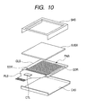
- FIG. 10 shows a projected perspective view of an organic EL display device to explain its configuration as a second example of an image display device of the present invention.
- FIG. 11 shows a plan view of the organic EL display device into which its components shown in FIG. 10 have been assembled.
- Organic EL elements are formed on the pixel electrodes comprised in the above-mentioned active matrix substrate GLS.
- the organic EL elements are formed of a laminate of a hole transport layer, light emitting layer, electron transport layer, and cathode metal layer deposited in series on the pixel electrode surface. Sealants are placed around the pixel area PAR where this laminate layer was formed on the active matrix substrate GLS and the laminate is sealed with a sealing substrate SUB or a sealing can.
- signals for display from an external signal source are supplied to a drain driving circuit region DDR, a gate driving circuit GDR, and other peripheral circuits CTL via a printed-circuit board (PLB). All components are packaged between a shield frame SHD as the upper case and the lower case CAS, thus fabricating the organic EL display device.
- PLB printed-circuit board
- the circuits formed in the drive circuit area are essential for high speed and high resolution.
- the active matrix substrate to which the present invention is applied has high performance fulfilling such requirements.
- the organic EL display device using that active matrix substrate is one of the display devices that maximize the features of the present embodiment.
- the present invention is not restricted to the above-described image display devices and not limited to the constitutions described in attached claims and the constitutions described in the embodiments and may be changed in various forms without departing the technical concept and idea of the present invention.
- the present invention is applicable to various types of semiconductor devices, not limited to semiconductor devices for image display.
- the present invention can also be applied to forming a semiconductor device in which circuits are simply formed. If the present invention is applied to simply form circuits on a substrate, all circuit regions can be formed with a semiconductor film crystallized by directly irradiating the amorphous silicon film with a CW laser light and the irradiation with a pulse excimer laser light can be dispensed with.
Landscapes
- Engineering & Computer Science (AREA)
- Physics & Mathematics (AREA)
- Power Engineering (AREA)
- Microelectronics & Electronic Packaging (AREA)
- Manufacturing & Machinery (AREA)
- Computer Hardware Design (AREA)
- General Physics & Mathematics (AREA)
- Condensed Matter Physics & Semiconductors (AREA)
- Chemical & Material Sciences (AREA)
- Crystallography & Structural Chemistry (AREA)
- Optics & Photonics (AREA)
- Liquid Crystal (AREA)
- Thin Film Transistor (AREA)
- Recrystallisation Techniques (AREA)
Applications Claiming Priority (2)
| Application Number | Priority Date | Filing Date | Title |
|---|---|---|---|
| JP2006-000618 | 2006-01-05 | ||
| JP2006000618A JP5232360B2 (ja) | 2006-01-05 | 2006-01-05 | 半導体装置及びその製造方法 |
Publications (2)
| Publication Number | Publication Date |
|---|---|
| US20070155070A1 US20070155070A1 (en) | 2007-07-05 |
| US7902003B2 true US7902003B2 (en) | 2011-03-08 |
Family
ID=38224967
Family Applications (1)
| Application Number | Title | Priority Date | Filing Date |
|---|---|---|---|
| US11/620,154 Expired - Fee Related US7902003B2 (en) | 2006-01-05 | 2007-01-05 | Semiconductor device and method for manufacturing the same |
Country Status (2)
| Country | Link |
|---|---|
| US (1) | US7902003B2 (ja) |
| JP (1) | JP5232360B2 (ja) |
Cited By (1)
| Publication number | Priority date | Publication date | Assignee | Title |
|---|---|---|---|---|
| TWI695381B (zh) * | 2018-09-06 | 2020-06-01 | 日商東芝記憶體股份有限公司 | 半導體記憶裝置及其製造方法 |
Families Citing this family (4)
| Publication number | Priority date | Publication date | Assignee | Title |
|---|---|---|---|---|
| SG156537A1 (en) | 2008-04-09 | 2009-11-26 | Toshiba Matsushita Display Tec | Methods of laser annealing a semiconductor layer and semiconductor devices produced thereby |
| KR20110114089A (ko) * | 2010-04-12 | 2011-10-19 | 삼성모바일디스플레이주식회사 | 박막 트랜지스터, 이의 제조 방법 및 이를 포함하는 표시 장치 |
| US20120001179A1 (en) * | 2010-07-02 | 2012-01-05 | Semiconductor Energy Laboratory Co., Ltd. | Semiconductor device |
| JP2023131583A (ja) * | 2022-03-09 | 2023-09-22 | 株式会社ブイ・テクノロジー | レーザアニール装置およびレーザアニール方法 |
Citations (5)
| Publication number | Priority date | Publication date | Assignee | Title |
|---|---|---|---|---|
| US5731613A (en) * | 1994-08-19 | 1998-03-24 | Semiconductor Energy Laboratory Co., Ltd. | Semiconductor device having a monocrystalline layer composed of carbon, oxygen, hydrogen and nitrogen atoms |
| JP2002368009A (ja) * | 2001-06-05 | 2002-12-20 | Matsushita Electric Ind Co Ltd | 薄膜トランジスタおよび液晶表示装置 |
| US20030042542A1 (en) * | 1996-04-26 | 2003-03-06 | Shigeto Maegawa | Semiconductor device having a thin film transistor and manufacturing method thereof |
| US20060001051A1 (en) * | 2004-07-01 | 2006-01-05 | Mitsuharu Tai | Thin film semiconductor circuit, manufacturing method thereof, and image display apparatus utilizing the same thin film semiconductor circuit |
| US20070004112A1 (en) * | 2005-06-30 | 2007-01-04 | Chia-Nan Shen | Method of forming thin film transistor and method of repairing defects in polysilicon layer |
Family Cites Families (3)
| Publication number | Priority date | Publication date | Assignee | Title |
|---|---|---|---|---|
| JP3103385B2 (ja) * | 1991-01-25 | 2000-10-30 | 株式会社東芝 | ポリシリコン薄膜半導体装置 |
| JP3134910B2 (ja) * | 1993-09-07 | 2001-02-13 | 株式会社半導体エネルギー研究所 | 半導体装置の作製方法および液晶ディスプレイ用集積回路の作製方法 |
| JP4474108B2 (ja) * | 2002-09-02 | 2010-06-02 | 株式会社 日立ディスプレイズ | 表示装置とその製造方法および製造装置 |
-
2006
- 2006-01-05 JP JP2006000618A patent/JP5232360B2/ja active Active
-
2007
- 2007-01-05 US US11/620,154 patent/US7902003B2/en not_active Expired - Fee Related
Patent Citations (5)
| Publication number | Priority date | Publication date | Assignee | Title |
|---|---|---|---|---|
| US5731613A (en) * | 1994-08-19 | 1998-03-24 | Semiconductor Energy Laboratory Co., Ltd. | Semiconductor device having a monocrystalline layer composed of carbon, oxygen, hydrogen and nitrogen atoms |
| US20030042542A1 (en) * | 1996-04-26 | 2003-03-06 | Shigeto Maegawa | Semiconductor device having a thin film transistor and manufacturing method thereof |
| JP2002368009A (ja) * | 2001-06-05 | 2002-12-20 | Matsushita Electric Ind Co Ltd | 薄膜トランジスタおよび液晶表示装置 |
| US20060001051A1 (en) * | 2004-07-01 | 2006-01-05 | Mitsuharu Tai | Thin film semiconductor circuit, manufacturing method thereof, and image display apparatus utilizing the same thin film semiconductor circuit |
| US20070004112A1 (en) * | 2005-06-30 | 2007-01-04 | Chia-Nan Shen | Method of forming thin film transistor and method of repairing defects in polysilicon layer |
Non-Patent Citations (1)
| Title |
|---|
| 12.4L Late-News paper: Selectively Enlarging laser Crystallization; Technology for High and Uniform Performance Poly-Si TFTs; M. Hatano et al. |
Cited By (1)
| Publication number | Priority date | Publication date | Assignee | Title |
|---|---|---|---|---|
| TWI695381B (zh) * | 2018-09-06 | 2020-06-01 | 日商東芝記憶體股份有限公司 | 半導體記憶裝置及其製造方法 |
Also Published As
| Publication number | Publication date |
|---|---|
| JP2007184358A (ja) | 2007-07-19 |
| US20070155070A1 (en) | 2007-07-05 |
| JP5232360B2 (ja) | 2013-07-10 |
Similar Documents
| Publication | Publication Date | Title |
|---|---|---|
| US7691545B2 (en) | Crystallization mask, crystallization method, and method of manufacturing thin film transistor including crystallized semiconductor | |
| US7183229B2 (en) | Semiconductor thin film forming method, production methods for semiconductor device and electrooptical device, devices used for these methods, and semiconductor device and electrooptical device | |
| JP5395384B2 (ja) | 薄膜トランジスタの作製方法 | |
| KR101518794B1 (ko) | 박막 트랜지스터의 제작 방법, 및 표시 장치의 제작 방법 | |
| KR100881992B1 (ko) | 반도체장치 제조방법 | |
| US5936291A (en) | Thin film transistor and method for fabricating the same | |
| US7790521B2 (en) | Thin film semiconductor device, method of manufacturing the same and display | |
| US20030010980A1 (en) | Semiconductor device and method for manufacturing same | |
| JP2009076894A (ja) | 表示装置及び表示装置の作製方法 | |
| JP2009049388A (ja) | 表示装置の作製方法 | |
| US8106409B2 (en) | Thin film transistor array panel | |
| US20070298553A1 (en) | Thin Film Transistor and Method For Production Thereof | |
| TWI446408B (zh) | 光罩與使用該光罩之薄膜電晶體陣列面板之製造方法 | |
| US8097883B2 (en) | Thin film transistors in pixel and driver portions characterized by surface roughness | |
| US7902003B2 (en) | Semiconductor device and method for manufacturing the same | |
| US20060006391A1 (en) | Image display devices | |
| JP5277020B2 (ja) | 表示装置 | |
| JP2009088106A (ja) | 半導体層とこの半導体層を用いた半導体装置および表示装置 | |
| US20040178452A1 (en) | Complementary thin film transistor circuit, electro-optical device, and electronic apparatus | |
| KR100915160B1 (ko) | 반도체 박막, 박막 트랜지스터, 그것들의 제조 방법 및반도체 박막의 제조 장치 | |
| JP2009302171A (ja) | 半導体装置の製造方法、トランジスタの製造方法ならびに電気光学装置の製造方法 | |
| US7026201B2 (en) | Method for forming polycrystalline silicon thin film transistor | |
| US8314428B2 (en) | Thin film transistor with LDD/offset structure | |
| KR20170041962A (ko) | 박막 트랜지스터 표시판의 제조 방법 및 박막 트랜지스터 표시판 | |
| JP5307992B2 (ja) | 表示装置の生産方法 |
Legal Events
| Date | Code | Title | Description |
|---|---|---|---|
| AS | Assignment |
Owner name: HITACHI DISPLAYS, LTD., JAPAN Free format text: ASSIGNMENT OF ASSIGNORS INTEREST;ASSIGNORS:OUCHI, KIYOSHI;HATANO, MATSUKO;SATO, TAKESHI;AND OTHERS;REEL/FRAME:018714/0820 Effective date: 20061215 |
|
| STCF | Information on status: patent grant |
Free format text: PATENTED CASE |
|
| AS | Assignment |
Owner name: PANASONIC LIQUID CRYSTAL DISPLAY CO., LTD., JAPAN Free format text: MERGER;ASSIGNOR:IPS ALPHA SUPPORT CO., LTD.;REEL/FRAME:027056/0914 Effective date: 20101001 Owner name: IPS ALPHA SUPPORT CO., LTD., JAPAN Free format text: COMPANY SPLIT PLAN TRANSFERRING FIFTY (50) PERCENT SHARE OF PATENTS;ASSIGNOR:HITACHI DISPLAYS, LTD.;REEL/FRAME:027056/0692 Effective date: 20100630 |
|
| FPAY | Fee payment |
Year of fee payment: 4 |
|
| MAFP | Maintenance fee payment |
Free format text: PAYMENT OF MAINTENANCE FEE, 8TH YEAR, LARGE ENTITY (ORIGINAL EVENT CODE: M1552); ENTITY STATUS OF PATENT OWNER: LARGE ENTITY Year of fee payment: 8 |
|
| FEPP | Fee payment procedure |
Free format text: MAINTENANCE FEE REMINDER MAILED (ORIGINAL EVENT CODE: REM.); ENTITY STATUS OF PATENT OWNER: LARGE ENTITY |
|
| LAPS | Lapse for failure to pay maintenance fees |
Free format text: PATENT EXPIRED FOR FAILURE TO PAY MAINTENANCE FEES (ORIGINAL EVENT CODE: EXP.); ENTITY STATUS OF PATENT OWNER: LARGE ENTITY |
|
| STCH | Information on status: patent discontinuation |
Free format text: PATENT EXPIRED DUE TO NONPAYMENT OF MAINTENANCE FEES UNDER 37 CFR 1.362 |
|
| FP | Lapsed due to failure to pay maintenance fee |
Effective date: 20230308 |