US7843004B2 - Power MOSFET with recessed field plate - Google Patents
Power MOSFET with recessed field plate Download PDFInfo
- Publication number
- US7843004B2 US7843004B2 US11/903,972 US90397207A US7843004B2 US 7843004 B2 US7843004 B2 US 7843004B2 US 90397207 A US90397207 A US 90397207A US 7843004 B2 US7843004 B2 US 7843004B2
- Authority
- US
- United States
- Prior art keywords
- rfp
- mosfet
- trench
- die
- gate
- Prior art date
- Legal status (The legal status is an assumption and is not a legal conclusion. Google has not performed a legal analysis and makes no representation as to the accuracy of the status listed.)
- Active, expires
Links
- 229910052751 metal Inorganic materials 0.000 claims description 24
- 239000002184 metal Substances 0.000 claims description 24
- 210000000746 body region Anatomy 0.000 claims description 19
- 229910021420 polycrystalline silicon Inorganic materials 0.000 claims description 13
- 229920005591 polysilicon Polymers 0.000 claims description 13
- 239000002019 doping agent Substances 0.000 claims description 11
- 239000004065 semiconductor Substances 0.000 claims description 5
- 238000002513 implantation Methods 0.000 claims 6
- 150000002500 ions Chemical class 0.000 claims 6
- 230000005684 electric field Effects 0.000 abstract description 7
- 238000011084 recovery Methods 0.000 abstract description 5
- 230000002301 combined effect Effects 0.000 abstract description 3
- 238000009792 diffusion process Methods 0.000 abstract description 3
- 238000000034 method Methods 0.000 description 19
- 230000015556 catabolic process Effects 0.000 description 11
- 239000000758 substrate Substances 0.000 description 9
- 229920002120 photoresistant polymer Polymers 0.000 description 7
- 229910052581 Si3N4 Inorganic materials 0.000 description 6
- VYPSYNLAJGMNEJ-UHFFFAOYSA-N Silicium dioxide Chemical compound O=[Si]=O VYPSYNLAJGMNEJ-UHFFFAOYSA-N 0.000 description 6
- HQVNEWCFYHHQES-UHFFFAOYSA-N silicon nitride Chemical compound N12[Si]34N5[Si]62N3[Si]51N64 HQVNEWCFYHHQES-UHFFFAOYSA-N 0.000 description 6
- 229910052796 boron Inorganic materials 0.000 description 5
- ZOXJGFHDIHLPTG-UHFFFAOYSA-N Boron Chemical compound [B] ZOXJGFHDIHLPTG-UHFFFAOYSA-N 0.000 description 4
- 239000004020 conductor Substances 0.000 description 4
- 150000004767 nitrides Chemical class 0.000 description 4
- 230000002441 reversible effect Effects 0.000 description 4
- OAICVXFJPJFONN-UHFFFAOYSA-N Phosphorus Chemical compound [P] OAICVXFJPJFONN-UHFFFAOYSA-N 0.000 description 3
- 229910052785 arsenic Inorganic materials 0.000 description 3
- RQNWIZPPADIBDY-UHFFFAOYSA-N arsenic atom Chemical compound [As] RQNWIZPPADIBDY-UHFFFAOYSA-N 0.000 description 3
- 238000005530 etching Methods 0.000 description 3
- 229910052698 phosphorus Inorganic materials 0.000 description 3
- 239000011574 phosphorus Substances 0.000 description 3
- 239000000377 silicon dioxide Substances 0.000 description 3
- WFKWXMTUELFFGS-UHFFFAOYSA-N tungsten Chemical compound [W] WFKWXMTUELFFGS-UHFFFAOYSA-N 0.000 description 3
- 229910052721 tungsten Inorganic materials 0.000 description 3
- 239000010937 tungsten Substances 0.000 description 3
- 239000005380 borophosphosilicate glass Substances 0.000 description 2
- 238000001312 dry etching Methods 0.000 description 2
- 238000002347 injection Methods 0.000 description 2
- 239000007924 injection Substances 0.000 description 2
- 239000011810 insulating material Substances 0.000 description 2
- 238000004519 manufacturing process Methods 0.000 description 2
- 235000012239 silicon dioxide Nutrition 0.000 description 2
- 238000001039 wet etching Methods 0.000 description 2
- BOTDANWDWHJENH-UHFFFAOYSA-N Tetraethyl orthosilicate Chemical compound CCO[Si](OCC)(OCC)OCC BOTDANWDWHJENH-UHFFFAOYSA-N 0.000 description 1
- 230000015572 biosynthetic process Effects 0.000 description 1
- 230000001413 cellular effect Effects 0.000 description 1
- 238000000151 deposition Methods 0.000 description 1
- 230000000694 effects Effects 0.000 description 1
- 239000007943 implant Substances 0.000 description 1
- 230000000873 masking effect Effects 0.000 description 1
- 238000012856 packing Methods 0.000 description 1
- 238000005498 polishing Methods 0.000 description 1
- 238000003892 spreading Methods 0.000 description 1
- 239000007858 starting material Substances 0.000 description 1
- 230000001360 synchronised effect Effects 0.000 description 1
Images


Classifications
-
- H—ELECTRICITY
- H01—ELECTRIC ELEMENTS
- H01L—SEMICONDUCTOR DEVICES NOT COVERED BY CLASS H10
- H01L29/00—Semiconductor devices adapted for rectifying, amplifying, oscillating or switching, or capacitors or resistors with at least one potential-jump barrier or surface barrier, e.g. PN junction depletion layer or carrier concentration layer; Details of semiconductor bodies or of electrodes thereof ; Multistep manufacturing processes therefor
- H01L29/40—Electrodes ; Multistep manufacturing processes therefor
- H01L29/402—Field plates
- H01L29/407—Recessed field plates, e.g. trench field plates, buried field plates
-
- H—ELECTRICITY
- H01—ELECTRIC ELEMENTS
- H01L—SEMICONDUCTOR DEVICES NOT COVERED BY CLASS H10
- H01L21/00—Processes or apparatus adapted for the manufacture or treatment of semiconductor or solid state devices or of parts thereof
- H01L21/02—Manufacture or treatment of semiconductor devices or of parts thereof
- H01L21/04—Manufacture or treatment of semiconductor devices or of parts thereof the devices having at least one potential-jump barrier or surface barrier, e.g. PN junction, depletion layer or carrier concentration layer
- H01L21/18—Manufacture or treatment of semiconductor devices or of parts thereof the devices having at least one potential-jump barrier or surface barrier, e.g. PN junction, depletion layer or carrier concentration layer the devices having semiconductor bodies comprising elements of Group IV of the Periodic System or AIIIBV compounds with or without impurities, e.g. doping materials
- H01L21/26—Bombardment with radiation
- H01L21/263—Bombardment with radiation with high-energy radiation
- H01L21/265—Bombardment with radiation with high-energy radiation producing ion implantation
- H01L21/26586—Bombardment with radiation with high-energy radiation producing ion implantation characterised by the angle between the ion beam and the crystal planes or the main crystal surface
-
- H—ELECTRICITY
- H01—ELECTRIC ELEMENTS
- H01L—SEMICONDUCTOR DEVICES NOT COVERED BY CLASS H10
- H01L29/00—Semiconductor devices adapted for rectifying, amplifying, oscillating or switching, or capacitors or resistors with at least one potential-jump barrier or surface barrier, e.g. PN junction depletion layer or carrier concentration layer; Details of semiconductor bodies or of electrodes thereof ; Multistep manufacturing processes therefor
- H01L29/02—Semiconductor bodies ; Multistep manufacturing processes therefor
- H01L29/06—Semiconductor bodies ; Multistep manufacturing processes therefor characterised by their shape; characterised by the shapes, relative sizes, or dispositions of the semiconductor regions ; characterised by the concentration or distribution of impurities within semiconductor regions
- H01L29/10—Semiconductor bodies ; Multistep manufacturing processes therefor characterised by their shape; characterised by the shapes, relative sizes, or dispositions of the semiconductor regions ; characterised by the concentration or distribution of impurities within semiconductor regions with semiconductor regions connected to an electrode not carrying current to be rectified, amplified or switched and such electrode being part of a semiconductor device which comprises three or more electrodes
- H01L29/1095—Body region, i.e. base region, of DMOS transistors or IGBTs
-
- H—ELECTRICITY
- H01—ELECTRIC ELEMENTS
- H01L—SEMICONDUCTOR DEVICES NOT COVERED BY CLASS H10
- H01L29/00—Semiconductor devices adapted for rectifying, amplifying, oscillating or switching, or capacitors or resistors with at least one potential-jump barrier or surface barrier, e.g. PN junction depletion layer or carrier concentration layer; Details of semiconductor bodies or of electrodes thereof ; Multistep manufacturing processes therefor
- H01L29/40—Electrodes ; Multistep manufacturing processes therefor
- H01L29/41—Electrodes ; Multistep manufacturing processes therefor characterised by their shape, relative sizes or dispositions
- H01L29/423—Electrodes ; Multistep manufacturing processes therefor characterised by their shape, relative sizes or dispositions not carrying the current to be rectified, amplified or switched
- H01L29/42312—Gate electrodes for field effect devices
- H01L29/42316—Gate electrodes for field effect devices for field-effect transistors
- H01L29/4232—Gate electrodes for field effect devices for field-effect transistors with insulated gate
- H01L29/42364—Gate electrodes for field effect devices for field-effect transistors with insulated gate characterised by the insulating layer, e.g. thickness or uniformity
- H01L29/42368—Gate electrodes for field effect devices for field-effect transistors with insulated gate characterised by the insulating layer, e.g. thickness or uniformity the thickness being non-uniform
-
- H—ELECTRICITY
- H01—ELECTRIC ELEMENTS
- H01L—SEMICONDUCTOR DEVICES NOT COVERED BY CLASS H10
- H01L29/00—Semiconductor devices adapted for rectifying, amplifying, oscillating or switching, or capacitors or resistors with at least one potential-jump barrier or surface barrier, e.g. PN junction depletion layer or carrier concentration layer; Details of semiconductor bodies or of electrodes thereof ; Multistep manufacturing processes therefor
- H01L29/66—Types of semiconductor device ; Multistep manufacturing processes therefor
- H01L29/66007—Multistep manufacturing processes
- H01L29/66075—Multistep manufacturing processes of devices having semiconductor bodies comprising group 14 or group 13/15 materials
- H01L29/66227—Multistep manufacturing processes of devices having semiconductor bodies comprising group 14 or group 13/15 materials the devices being controllable only by the electric current supplied or the electric potential applied, to an electrode which does not carry the current to be rectified, amplified or switched, e.g. three-terminal devices
- H01L29/66409—Unipolar field-effect transistors
- H01L29/66477—Unipolar field-effect transistors with an insulated gate, i.e. MISFET
- H01L29/66674—DMOS transistors, i.e. MISFETs with a channel accommodating body or base region adjoining a drain drift region
- H01L29/66712—Vertical DMOS transistors, i.e. VDMOS transistors
- H01L29/66734—Vertical DMOS transistors, i.e. VDMOS transistors with a step of recessing the gate electrode, e.g. to form a trench gate electrode
-
- H—ELECTRICITY
- H01—ELECTRIC ELEMENTS
- H01L—SEMICONDUCTOR DEVICES NOT COVERED BY CLASS H10
- H01L29/00—Semiconductor devices adapted for rectifying, amplifying, oscillating or switching, or capacitors or resistors with at least one potential-jump barrier or surface barrier, e.g. PN junction depletion layer or carrier concentration layer; Details of semiconductor bodies or of electrodes thereof ; Multistep manufacturing processes therefor
- H01L29/66—Types of semiconductor device ; Multistep manufacturing processes therefor
- H01L29/68—Types of semiconductor device ; Multistep manufacturing processes therefor controllable by only the electric current supplied, or only the electric potential applied, to an electrode which does not carry the current to be rectified, amplified or switched
- H01L29/76—Unipolar devices, e.g. field effect transistors
- H01L29/772—Field effect transistors
- H01L29/78—Field effect transistors with field effect produced by an insulated gate
- H01L29/7801—DMOS transistors, i.e. MISFETs with a channel accommodating body or base region adjoining a drain drift region
- H01L29/7802—Vertical DMOS transistors, i.e. VDMOS transistors
- H01L29/7803—Vertical DMOS transistors, i.e. VDMOS transistors structurally associated with at least one other device
- H01L29/7808—Vertical DMOS transistors, i.e. VDMOS transistors structurally associated with at least one other device the other device being a breakdown diode, e.g. Zener diode
-
- H—ELECTRICITY
- H01—ELECTRIC ELEMENTS
- H01L—SEMICONDUCTOR DEVICES NOT COVERED BY CLASS H10
- H01L29/00—Semiconductor devices adapted for rectifying, amplifying, oscillating or switching, or capacitors or resistors with at least one potential-jump barrier or surface barrier, e.g. PN junction depletion layer or carrier concentration layer; Details of semiconductor bodies or of electrodes thereof ; Multistep manufacturing processes therefor
- H01L29/66—Types of semiconductor device ; Multistep manufacturing processes therefor
- H01L29/68—Types of semiconductor device ; Multistep manufacturing processes therefor controllable by only the electric current supplied, or only the electric potential applied, to an electrode which does not carry the current to be rectified, amplified or switched
- H01L29/76—Unipolar devices, e.g. field effect transistors
- H01L29/772—Field effect transistors
- H01L29/78—Field effect transistors with field effect produced by an insulated gate
- H01L29/7801—DMOS transistors, i.e. MISFETs with a channel accommodating body or base region adjoining a drain drift region
- H01L29/7802—Vertical DMOS transistors, i.e. VDMOS transistors
- H01L29/7809—Vertical DMOS transistors, i.e. VDMOS transistors having both source and drain contacts on the same surface, i.e. Up-Drain VDMOS transistors
-
- H—ELECTRICITY
- H01—ELECTRIC ELEMENTS
- H01L—SEMICONDUCTOR DEVICES NOT COVERED BY CLASS H10
- H01L29/00—Semiconductor devices adapted for rectifying, amplifying, oscillating or switching, or capacitors or resistors with at least one potential-jump barrier or surface barrier, e.g. PN junction depletion layer or carrier concentration layer; Details of semiconductor bodies or of electrodes thereof ; Multistep manufacturing processes therefor
- H01L29/66—Types of semiconductor device ; Multistep manufacturing processes therefor
- H01L29/68—Types of semiconductor device ; Multistep manufacturing processes therefor controllable by only the electric current supplied, or only the electric potential applied, to an electrode which does not carry the current to be rectified, amplified or switched
- H01L29/76—Unipolar devices, e.g. field effect transistors
- H01L29/772—Field effect transistors
- H01L29/78—Field effect transistors with field effect produced by an insulated gate
- H01L29/7801—DMOS transistors, i.e. MISFETs with a channel accommodating body or base region adjoining a drain drift region
- H01L29/7802—Vertical DMOS transistors, i.e. VDMOS transistors
- H01L29/7813—Vertical DMOS transistors, i.e. VDMOS transistors with trench gate electrode, e.g. UMOS transistors
-
- H—ELECTRICITY
- H01—ELECTRIC ELEMENTS
- H01L—SEMICONDUCTOR DEVICES NOT COVERED BY CLASS H10
- H01L29/00—Semiconductor devices adapted for rectifying, amplifying, oscillating or switching, or capacitors or resistors with at least one potential-jump barrier or surface barrier, e.g. PN junction depletion layer or carrier concentration layer; Details of semiconductor bodies or of electrodes thereof ; Multistep manufacturing processes therefor
- H01L29/02—Semiconductor bodies ; Multistep manufacturing processes therefor
- H01L29/06—Semiconductor bodies ; Multistep manufacturing processes therefor characterised by their shape; characterised by the shapes, relative sizes, or dispositions of the semiconductor regions ; characterised by the concentration or distribution of impurities within semiconductor regions
- H01L29/0684—Semiconductor bodies ; Multistep manufacturing processes therefor characterised by their shape; characterised by the shapes, relative sizes, or dispositions of the semiconductor regions ; characterised by the concentration or distribution of impurities within semiconductor regions characterised by the shape, relative sizes or dispositions of the semiconductor regions or junctions between the regions
- H01L29/0692—Surface layout
- H01L29/0696—Surface layout of cellular field-effect devices, e.g. multicellular DMOS transistors or IGBTs
-
- H—ELECTRICITY
- H01—ELECTRIC ELEMENTS
- H01L—SEMICONDUCTOR DEVICES NOT COVERED BY CLASS H10
- H01L29/00—Semiconductor devices adapted for rectifying, amplifying, oscillating or switching, or capacitors or resistors with at least one potential-jump barrier or surface barrier, e.g. PN junction depletion layer or carrier concentration layer; Details of semiconductor bodies or of electrodes thereof ; Multistep manufacturing processes therefor
- H01L29/40—Electrodes ; Multistep manufacturing processes therefor
- H01L29/41—Electrodes ; Multistep manufacturing processes therefor characterised by their shape, relative sizes or dispositions
- H01L29/417—Electrodes ; Multistep manufacturing processes therefor characterised by their shape, relative sizes or dispositions carrying the current to be rectified, amplified or switched
- H01L29/41725—Source or drain electrodes for field effect devices
- H01L29/41766—Source or drain electrodes for field effect devices with at least part of the source or drain electrode having contact below the semiconductor surface, e.g. the source or drain electrode formed at least partially in a groove or with inclusions of conductor inside the semiconductor
-
- H—ELECTRICITY
- H01—ELECTRIC ELEMENTS
- H01L—SEMICONDUCTOR DEVICES NOT COVERED BY CLASS H10
- H01L2924/00—Indexing scheme for arrangements or methods for connecting or disconnecting semiconductor or solid-state bodies as covered by H01L24/00
- H01L2924/10—Details of semiconductor or other solid state devices to be connected
- H01L2924/11—Device type
- H01L2924/13—Discrete devices, e.g. 3 terminal devices
- H01L2924/1304—Transistor
- H01L2924/1306—Field-effect transistor [FET]
- H01L2924/13091—Metal-Oxide-Semiconductor Field-Effect Transistor [MOSFET]
Definitions
- Power MOSFETs are widely used as switching devices in many electronic applications. In order to minimize conduction power loss it is desirable that power MOSFETs have a low specific on-resistance, which is defined as the product of the on-resistance (Ron) of the MOSFET multiplied by the active die area (A) of the MOSFET (Ron*A).
- Ron on-resistance
- a trench-type MOSFET as shown in the schematic cross-sectional view of a MOSFET 10 in FIG. 1 , provides a low specific on-resistance because of its high packing density or number of cells per unit area.
- the associated capacitances such as the gate-to-source capacitance (Cgs), the gate-to-drain capacitance (Cgd), and the drain-to-source capacitance (Cds), also increase.
- Cgs gate-to-source capacitance
- Cgd gate-to-drain capacitance
- Cds drain-to-source capacitance
- MOSFETs with a breakdown voltage in the range of 12 to 30V are required to operate at switching frequencies approaching 1 MHz. Therefore, it is desirable to minimize the switching or dynamic power loss caused by these capacitances.
- the magnitudes of these capacitances are directly proportional to the gate charge (Qg), the gate-drain charge (Qgd), and output charge (Qoss).
- U.S. Pat. No. 6,710,403 to Sapp proposes a dual-trench power MOSFET, as shown in FIG. 2 , with two deeper polysilicon-filled trenches 22 on either side of an active trench 24 , to lower the levels of Ron, Cgs and Cgd.
- MOSFET 20 does not lower the reverse recovery charge Qrr and requires the fabrication of trenches having two different depths.
- the deep and shallow trenches are not self-aligned, which causes variations in mesa widths and hence in breakdown voltages.
- a MOSFET according to the invention is formed in a semiconductor die and comprises a gate trench and a recessed field plate (RFP) trench that are self-aligned, both trenches extending from a surface of the die and forming a mesa between them.
- the gate trench comprises a gate electrode separated from the die by a first dielectric layer having a thick section at the bottom of the gate trench and extends to substantially the same depth as the RFP trench.
- the RFP trench contains an RFP electrode separated from the die by a second dielectric layer.
- the MOSFET also comprises a source region of a first conductivity type adjacent the surface of the die and a sidewall of the gate trench and adjacent to the RFP electrode trench in some areas of the MOSFET and a body region of a second conductivity type opposite to the first conductivity type adjacent the sidewall of the gate trench and the source region.
- a p+ body contact region may be placed laterally adjacent to the P ⁇ body.
- the RFP electrode may be independently biased or may be biased at the source potential
- the respective depths of the gate and RFP trenches are substantially the same.
- the invention also comprises a method of fabricating a MOSFET.
- the method comprises providing a semiconductor die; etching the die so as to form a gate trench and a recessed field plate (RFP) trench, the gate trench and the RFP trench extending from a surface of the die and being of substantially equal depth; forming an insulating layer at a bottom of the gate trench; forming a gate dielectric layer on a sidewall of the gate trench above the insulating layer; forming a second dielectric layer along the walls of the RFP trench; introducing conductive material into the gate trench to form a gate electrode; introducing conductive material into the RFP trench to form an RFP electrode; implanting dopant of a second conductivity type opposite to the first conductivity type to form a body region in the mesa adjacent the sidewall of the gate trench; implanting dopant of a first conductivity type to form a source region adjacent the surface of the die in the mesa; and depositing a source contact layer on the surface of the die in contact with the
- FIG. 1 is a cross-sectional view of a conventional trench-type MOSFET.
- FIG. 2 is a cross-sectional view of a known dual-trench MOSFET.
- FIG. 3A is a cross-sectional view of a MOSFET having a recessed field plate (RFP) in accordance with the invention, with the recessed field plate (RFP) electrode independently biased.
- RFP recessed field plate
- FIG. 3B is a cross-sectional view of a MOSFET having a recessed field plate (RFP) in accordance with the invention, with the RFP electrode biased at the same potential as the source.
- RFP recessed field plate
- FIG. 4A is a top view of the MOSFET shown in FIG. 3A .
- FIG. 4B is a cross-sectional view of the MOSFET shown in FIG. 3A , taken at cross-section 4 B- 4 B in FIG. 4A .
- FIG. 5A is a cross-sectional view of an alternative embodiment wherein the RFP electrode is in contact with the source region.
- FIG. 5B is a cross-sectional view of the MOSFET of FIG. 5A taken at a cross-section corresponding to cross-section 4 B- 4 B in FIG. 4A .
- FIGS. 6A-6H illustrate a process of fabricating the MOSFET shown in FIG. 3A .
- FIGS. 7A and B illustrate an alternative version of a portion of the process shown in FIGS. 6A-6H .
- FIGS. 8A and 8B are cross-sectional views of a MOSFET according to the invention wherein an insulating layer above the gate trench overlaps a portion of the source regions and the source contact layer contacts the RFP electrodes.
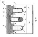
- FIG. 9 is a cross-sectional view of a MOSFET similar to the MOSFET of FIGS. 8A and 8B wherein body contact regions are formed laterally adjacent to the source regions.
- FIG. 10 is a cross-sectional view of an MOSFET similar to the MOSFET of FIG. 9 wherein the body contact regions extend to a level below the source regions.
- FIG. 11 is a cross-sectional view of a MOSFET according to the invention wherein the RFP electrodes are recessed and body contact regions are formed laterally adjacent to the body regions.
- FIG. 12 is a cross-sectional view of a MOSFET similar to the MOSFET of FIG. 11 wherein the body contact regions extend to a level below the body regions.
- FIG. 13 is a cross-sectional view of a MOSFET similar to the MOSFET of FIG. 12 wherein metal plugs are formed in the upper portions of the RFP trenches.
- FIGS. 14A-14H illustrate a process of fabricating the MOSFET shown in FIG. 10 .
- FIGS. 15A and 15B illustrate a variation of the process shown in FIGS. 14A-14H .
- FIGS. 16A and 16B are cross-sectional views of MOSFETs according to the invention that contain deep p-type regions to limit the breakdown voltage of the MOSFET.
- FIG. 17 is a cross-sectional view of a MOSFETs according to the invention wherein the RFP trenches contain a thick bottom oxide layer.
- FIGS. 18A-18C are cross-sectional views of MOSFETs containing a stepped oxide layer in the gate trench and/or the RFP trenches.
- FIG. 19 is a cross-sectional view of a MOSFET wherein the gate trench is deeper than the RFP trenches.
- FIG. 20 is a cross-sectional view of a quasi-vertical MOSFET in accordance with the invention.
- MOSFET 30 is formed in a semiconductor die comprising an n-type epitaxial layer 36 that is grown over a heavily doped n+ substrate 38 .
- MOSFET 30 includes recessed field plate (RFP) trenches 32 A and 32 B located on either side a gate trench 34 in the n-type epitaxial layer 36 .
- RFP recessed field plate
- the thick bottom oxide of the gate trench 34 extends to substantially the same depth as the RFP trenches 32 A and 32 B.
- the RFP trenches 32 A and 32 B and the gate trench 34 are preferably formed in the same processing step and therefore are self-aligned (i.e., the RFP trenches 32 A and 32 B are equally spaced from gate trench 34 regardless of processing and alignment variations), and RFP trenches 32 A and 32 B and gate trench 34 are of equal or substantially equal depth (e.g., the respective depths of RFP trenches 32 A and 32 B are within +/ ⁇ 10%, or preferably +/ ⁇ 5%, of the depth of gate trench 32 ).
- the mesas between the trenches contain n+ source regions 37 and p-body regions 39 , and below p-body regions 39 is an n-type drain-drift region 41 of epitaxial layer 36 .
- the drain-drift region 41 includes areas 41 A between RFP trenches 32 A and 32 B and gate trench 34 .
- the drain-drift region 41 and the n+ substrate 38 together form the drain 43 of MOSFET 30 .
- MOSFET 20 when the body-drain junction is reverse-biased, the electric field strength is reduced and hence the breakdown voltage is increased due to the spread of the depletion region between the two deep trenches 22 , mainly in the drift region below the gate trench 24 .
- MOSFET 30 under the same conditions the electric field is further reduced because the depletion layer is initially limited to the narrower areas 41 A of drain-drift region 41 located between the thick oxide of the gate trench 34 and RFP trenches 32 A and 32 B.
- trenches 32 A and 32 B are lined with a layer 33 of an insulating material such as silicon dioxide (SiO 2 ) and trenches 32 A and 32 B contain RFP electrodes 35 , each of which comprises a layer of a conductive material such as n-type or p-type doped polysilicon.
- the oxide layer 33 preferably has a breakdown voltage that exceeds the breakdown voltage of MOSFET 30 .
- the gate trench 34 is filled with a layer 40 of insulating material up to the level of the p-n junctions between p-body regions 39 and the drain-drift region 41 of epitaxial layer 36 .
- insulating layer 40 Above insulating layer 40 is a gate electrode 42 , which may be formed of n-type doped polysilicon and which is separated from epitaxial layer 36 by a gate dielectric layer 44 . Channel regions 45 (represented by the dashed lines) lie within the p-body regions 39 adjacent the gate dielectric layer 44 .
- the thickness of insulating layer 40 is preferably set so as to minimize the overlap of the gate electrode 42 and the drain-drift region 41 .
- An overlying source contact layer 46 contacts n+ source regions 37
- a drain contact layer 31 contacts n+ substrate 38 .
- Contact layers 46 and 31 are typically formed of a metal although they could also be formed of another conductive material.
- RFP electrodes 35 in RFP trenches 32 A and 32 B extend to a level that is deeper below the surface 36 A of epitaxial layer 36 than the bottom of gate electrode 42 .
- RFP electrodes 35 may be independently biased or, as shown in FIG. 3B , may be connected to n+ source regions 37 outside the plane of the drawing.
- the doping concentration of the drain-drift region 41 in the areas between the RFP trenches 32 A and 32 B and the gate trench 34 is less (e.g., 5 ⁇ 10 15 to 1.5 ⁇ 10 16 cm ⁇ 3 ) than the doping concentration of the drain-drift region 41 in the area below the gate trench 34 (e.g., 2 ⁇ 10 16 to 3 ⁇ 10 16 cm ⁇ 3 ).
- This structure improves depletion-spreading in the areas of drain-drift region 41 A between the RFP trenches 32 A and 32 B and the gate trench 34 when the PN junction between the body region 39 and the drain-drift region 41 is reverse-biased due to the limited depletion charge in region 41 A.
- n+ source regions 37 extend between the gate trench 34 and the RFP trenches 32 A and 32 B.
- a MOSFET 50 shown in the top view of FIG. 4A and the cross-sectional view of FIG. 4B , is similar to MOSFET 30 , but in selected areas the n+ source regions 37 are replaced by p+ body contact regions 52 so as to avoid snap-back or second breakdown characteristics.
- FIG. 4A the view at cross-section 3 A- 3 A is identical to cross-sectional view shown in FIG. 3A , and the view at cross-section 4 B- 4 B is shown in FIG. 4B .
- a conventional N-channel MOSFET When a conventional N-channel MOSFET operates in the third quadrant, its drain is negatively biased with respect to its source-body electrode, and the diffusion current results in minority carrier injection and a high Qrr.
- MOSFETs 30 and 50 because the n+ source regions 37 extend all the way across the mesa between the gate trench 34 and the RFP trenches 32 A and 32 B, the RFP electrodes 35 provide a majority carrier channel current path from drain to source in addition to that provided by the gate electrode in the conventional structure.
- the combined effect of the RFP and gate electrodes results in a significant reduction in the minority carrier diffusion current and reverse recovery charge Qrr than in conventional structures.
- the RFP electrode acts as an additional gate without the penalty of the added gate-drain capacitance (Cgd) and gate-source capacitance (Cgs).
- the RFP electrodes 35 also function as a recessed field plates to reduce the electric field in the channel regions 45 when MOSFETs 30 and 50 are reverse-biased. This effect enables the use of shorter channel lengths, without concern about punchthrough breakdown, and this results in a lower specific on-resistance (Ron*A) and a lower gate charge (Qg).
- Ron*A specific on-resistance
- Qg gate charge
- the drift regions 41 A below p ⁇ body regions 39 are constrained between the thick gate bottom oxide and the RFP electrode and are therefore more effectively depleted. Therefore, a deeper depletion layer results for the same reverse bias body-drain junction conditions, and a shorter channel can be used, resulting in a lower on-resistance.
- the gate-to-drain capacitance (Cgd) drops at a faster rate with applied drain-source voltage Vds, a lower gate-drain charge Qgd and a better Ron-Qgd trade-off are realized.
- the combined effect of the RFP electrodes 35 and of having the gate trench 34 filled with insulating layer 40 up to the junctions between the p-body regions 39 and the drain-drift region 41 helps to deplete area of the drain-drift region 36 between the trenches 32 A, 32 B and 34 at a higher rate as the drain-source voltage Vds is increased while MOSFETs 30 and 50 are in the off-state.
- a lower gate-drain charge (Qgd) results because of the low gate-to-drain capacitance (Cgd) and its fast falling rate with increasing Vds.
- the doping in the p-body regions 39 can be adjusted to obtain a lower threshold voltage at the same breakdown or punchthrough voltage.
- the doping in the p-body regions 39 can be further adjusted so that the p-body regions 39 are fully depleted, which significantly reduces gate charge Qg.
- FIGS. 3A and 3B the RFP electrodes 35 are separated from the source contact layer 46 by an insulating layer 48 .
- a MOSFET 60 shown in FIGS. 5A and 5B , there is no insulating layer 48 , and RFP electrodes 62 in RFP trenches 64 A and 64 B extend upward to electrically contact the source contact layer 46 .
- FIG. 5A is a view taken at a cross-section corresponding to cross-section 3 A- 3 A in FIG. 4A
- FIG. 5B is a view taken at a cross-section corresponding to cross-section 4 B- 4 B in FIG. 4A
- FIGS. 6A-6H An exemplary process for fabricating MOSFET 30 of FIG. 3A is shown in FIGS. 6A-6H .
- the starting material is the heavily-doped n+ substrate 38 , which may be doped, for example, with phosphorus or arsenic.
- the n-type epitaxial layer 36 is grown on top of the n+ substrate 38 .
- a thin oxide layer 72 is grown over the n-type epitaxial layer 36 , and a silicon nitride layer 74 is deposited on top of the oxide layer 72 .
- the oxide layer 72 can be 200-300 A thick, and the silicon nitride layer 74 can be 1000 A thick.
- a photoresist mask (not shown) is used to pattern the silicon nitride layer 74 and oxide layer 72 with openings 76 , as shown in FIG. 6B .
- the epitaxial layer 36 is etched through the openings 76 to form the RFP trenches 32 A and 32 B and the gate trench 34 , as shown in FIG. 6C .
- trenches 32 A, 32 B and 34 are illustrative only; typically numerous trenches would be formed.
- a thin thermal oxide layer (not shown), for example, 300 A thick, is grown on the walls of trenches 32 A, 32 B and 34 , and trenches 32 A, 32 B and 34 are then filled with a layer 78 of deposited silicon dioxide such as LTO or TEOS or high density plasma (HDP) oxide.
- the resulting structure is shown in FIG. 6C .
- the oxide layer 78 is etched back using a dry plasma etch or chemical-mechanical polishing (CMP) technique to a level the same as or slightly below the top surface of the silicon nitride layer 74 .
- a photoresist mask layer 80 is deposited and patterned to form openings 82 over the RFP trenches 32 A and 32 B, as shown in FIG. 6D , and the oxide layer 78 in the RFP trenches 32 A and 32 B is then completely or partially etched through the openings 82 by a wet or a dry plasma etch or a combination of wet and dry etching to yield the structure shown in FIG. 6D .
- Silicon nitride layer 74 prevents epitaxial layer 36 from being etched.
- the photoresist mask layer 80 is removed and the portion of oxide layer 78 remaining in the gate trench 34 is partially etched by wet etching. At the same time, the remaining portion of oxide layer 78 at the bottom of the RFP trenches 32 A and 32 B is removed. This is followed by an etch to remove the silicon nitride layer 74 and a wet oxide etch to remove the oxide layer 72 and any remaining oxide on the walls of the RFP trenches 32 A and 32 B. The resulting structure is shown in FIG. 6E .
- a thermal process is then performed to form oxide layer 33 on the walls of the RFP trenches 32 A and 32 B and gate dielectric layer 44 on the walls of the gate trench 34 above the remaining portion of the oxide layer 78 (which forms the insulating layer 40 at the bottom of the gate trench 34 ).
- This process also creates an oxide layer 80 on the top surface of the epitaxial layer 36 .
- These oxide layers could have a thickness, for example, in the range of 200 A to 1000 A.
- a layer 82 of polysilicon is then deposited and then doped, for example, by implanting with an n-type dopant such as phosphorus and then etched back to a level at or below that of the surface of oxide layer 80 by a plasma dry etching or CMP technique.
- Several masking and implant steps are performed to form the p-body regions 39 and p+ body contact regions 52 (shown in FIGS. 4A and 4B ), using a p-type dopant such as boron, and to form the n+ source regions 37 , using an n-type dopant such as arsenic or phosphorus or a combination thereof.
- a deep p layer (not shown) may also be implanted at this step or earlier in the process.
- the polysilicon layer 82 is etched back and an oxide layer is deposited and later etched, leaving the RFP electrodes 35 and the gate electrode 42 covered by an oxide layer 84 , as shown in FIG. 6G
- the source contact layer 46 is deposited and defined by a photoresist mask (not shown).
- the back side of the n+ substrate 38 is thinned and the drain metal layer 31 deposited, resulting in the MOSFET 30 shown in FIGS. 3A and 6H .
- oxide layer 78 remaining in RFP trenches 32 A and 32 B and in gate trench 34 are etched, and the steps shown in FIGS. 7A and 7B are performed.
- oxide layer 72 and nitride layer 74 still in place oxide layers 33 and 44 are thermally grown on the walls of the RFP and gate trenches 32 A/ 32 B and 34 , respectively.
- a polysilicon layer 85 is deposited and partially removed by etching or CMP so that the surface of the polysilicon layer 85 is level with or below the surface of the nitride layer 74 . The resulting structure is shown in FIG. 7A .
- the polysilicon layer 85 is etched (e.g., by about 0.1 ⁇ m) and an oxide layer 87 is deposited and etched back so that the surface of oxide layer 87 is level with or below the nitride layer 74 .
- Nitride layer 74 is removed by etching and optionally oxide layer 72 may be removed and a sacrificial oxide layer (not shown) may be re-grown.
- P-body regions 39 and n+ source regions 37 are implanted.
- Oxide layer 87 is then removed from the areas over the n+ source regions 37 , leaving the structure shown in FIG. 7B .
- a source contact layer (not shown) is then deposited on top of the oxide layer 87 and n+ source regions 37 .
- FIG. 8A is another view of MOSFET 70 , taken at a cross-section similar to cross-section 4 B- 4 B shown in FIG. 4A , where the n+ source regions are replaced by p+ body contact regions 52 .
- a MOSFET 80 shown in FIG. 9 , is similar to MOSFET 70 except that p+ body contact regions 96 are formed adjacent to n+ source regions 98 at the surface 36 A of epitaxial layer 36 to provide a source-body short via source contact layer 94 .
- MOSFET 80 it would not be necessary to interrupt the n+ source regions with p+ body contact regions 52 as shown in FIG. 4A to provide a source-body short.
- MOSFET 90 shown in FIG. 10 , is similar to MOSFET 80 except that p+ body contact regions 99 extend to a level below the bottoms of n+ source regions to provide a larger surface along the walls of RFP trenches 32 A and 32 B for contact with source contact layer 94 .
- a process for making MOSFET 90 is shown in FIGS. 14A-14H .
- p+ body contact regions 104 are formed below the n+ source regions 37 and adjacent to the p-body regions 106 .
- the bottom junctions of p-body regions 106 and p+ body contact regions 104 are at approximately the same level in epitaxial layer 36 .
- the RFP electrodes 112 and the oxide layers 110 are recessed sufficiently to permit the source contact layer 108 to contact the p+ body contact regions 104 , thereby providing a source-body short.
- insulating layer 92 extends above the surface 36 A of epitaxial layer 36 and covers the n+ source regions 37 .
- MOSFET 100 may allow for a higher cell density and therefore a lower specific on-resistance.
- MOSFET 110 shown in FIG. 12 , is similar to MOSFET 100 except that p+ body contact regions 114 extend to a level below the bottom of p-body regions 106 .
- MOSFET 120 shown in FIG. 13 , is similar to MOSFET 110 except that RFP trenches 118 A and 118 B contain metal plugs 116 , comprising for example tungsten, which contact both the source regions 37 and the p+ body contact regions 114 to provide a very low-resistance conduction path between source regions 37 and p+ body contact regions 114 .
- FIGS. 14A-14H illustrate a process of fabricating MOSFET 90 , shown in FIG. 10 .
- the process starts with growing n-type epitaxial layer 36 on top of n+ substrate 38 .
- an oxide layer 120 e.g., 0.5 ⁇ m thick
- a photoresist trench mask layer 122 are deposited over the top surface of epitaxial layer 36 .
- Mask layer 122 is patterned to form openings and oxide layer 120 and epitaxial layer 36 are etched through the openings to form RFP trenches 32 A and 32 B and gate trench 34 .
- the mask layer 122 and oxide layer 120 are removed, and a sacrificial oxide layer and a pad oxide layer (not shown) are grown.
- an oxide layer 124 is deposited in trenches 32 A, 32 B and 34 .
- Oxide layer 124 is preferably a high quality oxide, such as a high-density plasma oxide.
- An active mask (not shown) is deposited and patterned with an opening over the active areas of the die, and oxide layer 124 is etched down into trenches 32 A, 32 B and 34 , as shown in FIG. 14C .
- the active mask prevents optional field termination oxide (not shown) or oxide layer 124 from being etched in the termination areas of the die.
- a photoresist bottom oxide (BOX) mask layer 126 is deposited and patterned with openings over the RFP trenches 32 A and 32 B, and the remains of oxide layer 124 is removed from RFP trenches 32 A and 32 B, leaving the remains of oxide layer 124 (which becomes insulating layer 40 ) in the bottom of gate trench 34 .
- the resulting structure is shown in FIG. 14D .
- BOX mask layer 126 is removed and, as shown in FIG. 14E , an oxide layer 128 is grown, resulting in the formation of oxide layer 33 on the walls of RFP trenches 32 A and 32 B and oxide layer 44 on the walls of gate trench 34 above insulating layer 40 .
- a polysilicon layer 130 is deposited (e.g., 7000 A thick) and a mask layer (not shown) is deposited and patterned, and polysilicon layer 130 is etched back into trenches 32 A, 32 B and 34 using CMP and/or a dry etch process, thereby forming the gate electrode 42 in gate trench 34 and the RFP electrodes 35 in RFP trenches 32 A and 32 B.
- a p-type dopant is implanted to form p-body regions 39 (e.g., boron at a dose of 5 ⁇ 10 12 cm ⁇ 2 and an energy of 100 keV).
- a rapid thermal anneal (RTA) process may be performed at a temperature of 1025° C. for 30 seconds, for example, resulting in a junction depth of 0.5 ⁇ m for p-body regions 39 .
- a photoresist source mask layer 132 is deposited and patterned to form an opening, and an n-type dopant is implanted to form n+ source regions 98 at the surface of epitaxial layer 36 adjacent to gate trench 34 .
- arsenic may be implanted at a dose of 2 ⁇ 10 15 cm ⁇ 2 and an energy of 80 keV to provide a junction depth of 0.2 ⁇ m for n+ source regions 98 and a channel length (L) of 0.25-0.3 ⁇ m.
- Source mask layer 132 is removed and, as shown in FIG. 14G , an inter-level dielectric (ILD) layer 136 —e.g., low-temperature oxide (LTO) and borophosphosilicate glass (BPSG)—is deposited to a thickness of 0.5-1.5 ⁇ m, for example. ILD layer 136 may then be densified.
- ILD inter-level dielectric
- a contact mask layer (not shown) is deposited on ILD layer 136 and patterned with openings over RFP trenches 32 A and 32 B, and ILD layer 136 and portions of RFP electrodes 35 are dry or wet etched through the openings in the contact mask layer.
- a reflow process may be performed on ILD layer 136 .
- a p-type dopant is implanted to form p+ body contact regions 99 .
- boron may be implanted at a dose of 1 ⁇ 10 15 cm ⁇ 2 to 4 ⁇ 10 15 cm ⁇ 2 and an energy of 20-60 keV to produce a junction depth of 0.4 ⁇ m for p+ body contact regions 99 .
- Source contact layer 94 is then deposited in contact with the RFP electrodes 35 , resulting in MOSFET 90 .
- tungsten plugs may be formed in the upper portions of RFP trenches 32 A and 32 B in contact with RFP electrodes 35 before source contact layer 94 is deposited.
- the polysilicon layer 130 is etched further down into RFP trenches 32 A and 32 B through the openings in the contact mask layer, forming RFP electrodes 112 .
- a p-type dopant such as boron is then implanted at an angle, forming p+ body contact regions 114 that are located below n+ source regions 37 and may extend further into the epitaxial layer 36 than the bottoms of p-body regions 106 .
- metal plugs 116 comprising tungsten, for example, may be formed in the upper portions of RFP trenches 32 A and 32 B before source contact layer 94 is deposited. Except for the presence of the metal plugs 116 , MOSFET 130 is similar to MOSFET 110 , shown in FIG. 12 .
- a deeper p region is formed in selected areas of the MOSFET to clamp its breakdown voltage to a predetermined value that is lower than the breakdown voltage of the RFP trench or other points in the device.
- MOSFET 150 shown in FIG. 16A
- deep p+ regions 152 are located outside of the areas between the RFP trenches 32 A and 32 B and the gate trench 34 .
- MOSFET 160 shown in FIG. 16B
- deep p+ regions 162 are located on both sides of each of the RFP trenches 32 A and 32 B.
- P+ regions 152 and 162 extend deeper into the epitaxial layer 36 than the p-body regions 39 and may be as deep as the RFP trenches 32 A and 32 B and the gate trench 34 . It should be noted that FIGS. 16A and 16B are taken at cross-sections where there is no n+ source region.
- the insulating layers lining the RFP trenches are thicker at the bottoms of the trenches than on the sides of the trenches.
- the insulating layer 172 lining the walls of RFP trenches 32 A and 32 B includes a section 172 B at the bottom of the trench that is thicker than a section 172 A along the sidewalls of the trench.
- the doping of the N-epitaxial drain-drift region 41 of the epitaxial layer 36 is non-uniform (see FIG. 3A ).
- the doping of drain-drift region 41 may be non-uniform, with the doping concentration increasing with increasing depth in the epitaxial layer 36 so that the doping concentration in the areas 41 A of drain-drift region 41 is less than the doping concentration in the portion of drain-drift region 41 below areas 41 A.
- the gate oxide layer 182 in gate trench 34 includes a thinner section 182 B, having a thickness d 1 , on the sidewalls of the trench 34 adjacent to the p-body regions 39 and a thicker section 182 A, having a thickness d 2 , along the lower sidewalls and bottom of the trench 34 .
- the thickness d 2 is less than one-half the width W of the trench 34 , so that the gate oxide layer 182 forms a “keyhole” shape.
- the thinner section 182 B and the thicker section 182 A are joined at a location adjacent to the junction between the p-body regions 39 and the drain-drift region 41 .
- the oxide layer 192 in each of the RFP trenches 32 A and 32 B includes a thinner section 192 B, having a thickness d 3 , on the upper sidewalls of the trenches 32 A and 32 B and a thicker section 192 A, having a thickness d 4 , along the lower sidewalls and bottom of the trenches 32 A and 32 B.
- the thickness d 4 is less than one-half the width W of the trenches 32 A and 32 B, so that the oxide layer 192 forms a “keyhole” shape.
- the gate trench 34 contains the gate oxide layer 182 (as described above) and the RFP trenches 32 A and 32 B contain the oxide layer 192 (as described above).
- the gate trench 214 is deeper than the RFP trenches 212 A and 212 B to reduce the electric field at the RFP trenches 212 A and 212 B, while the gate electrode 216 is shallower than the RFP electrodes 215 .
- gate trench 214 extends to a deeper level in epitaxial layer 36 than the bottoms of RFP trenches 212 A and 212 B but owing to the thickness of insulating layer 40 at the bottom of the gate trench 216 RFP electrodes 215 extend to a deeper level than gate electrode 216 .
- FIG. 20 is a cross-sectional view of a quasi-vertical MOSFET 220 .
- MOSFET 220 includes a gate trench 224 , RFP trenches 222 A and 222 B, n+ source regions 226 and p-body regions 228 .
- An n-buried layer 230 is formed at the interface between a p-type substrate 236 and an n-epitaxial layer 234 .
- N-buried layer 230 is contacted from the top surface of n-epitaxial layer 234 via n+ sinker regions 232 .
- RFP electrodes 235 in RFP trenches 222 A and 222 B are contacted by a source contact layer 238 .
- MOSFET 220 When MOSFET 220 is turned on, a current flows from n+ source regions 226 , through p-body regions 228 to n-buried layer 230 and back up to the surface of n-epitaxial layer 234 via n+ sinker regions 232 .
- devices in accordance with this invention may be fabricated in various layouts, including “stripe” and “cellular” layouts.
- the embodiments described above have generally been n-channel MOSFETs, the principles of this invention are equally applicable to p-channel MOSFETs.
- the embodiments described above include an epitaxial layer grown on a substrate, in some embodiments the epitaxial layer may be omitted. It should also be noted that various combinations of the above embodiments can be realized and are included within the scope of this disclosure.
Abstract
Description
Claims (27)
Priority Applications (2)
| Application Number | Priority Date | Filing Date | Title |
|---|---|---|---|
| US11/903,972 US7843004B2 (en) | 2006-09-27 | 2007-09-25 | Power MOSFET with recessed field plate |
| US12/912,811 US20110039384A1 (en) | 2006-09-27 | 2010-10-27 | Power MOSFET With Recessed Field Plate |
Applications Claiming Priority (2)
| Application Number | Priority Date | Filing Date | Title |
|---|---|---|---|
| US84755106P | 2006-09-27 | 2006-09-27 | |
| US11/903,972 US7843004B2 (en) | 2006-09-27 | 2007-09-25 | Power MOSFET with recessed field plate |
Related Child Applications (1)
| Application Number | Title | Priority Date | Filing Date |
|---|---|---|---|
| US12/912,811 Division US20110039384A1 (en) | 2006-09-27 | 2010-10-27 | Power MOSFET With Recessed Field Plate |
Publications (2)
| Publication Number | Publication Date |
|---|---|
| US20080073707A1 US20080073707A1 (en) | 2008-03-27 |
| US7843004B2 true US7843004B2 (en) | 2010-11-30 |
Family
ID=39230511
Family Applications (2)
| Application Number | Title | Priority Date | Filing Date |
|---|---|---|---|
| US11/903,972 Active 2028-10-17 US7843004B2 (en) | 2006-09-27 | 2007-09-25 | Power MOSFET with recessed field plate |
| US12/912,811 Abandoned US20110039384A1 (en) | 2006-09-27 | 2010-10-27 | Power MOSFET With Recessed Field Plate |
Family Applications After (1)
| Application Number | Title | Priority Date | Filing Date |
|---|---|---|---|
| US12/912,811 Abandoned US20110039384A1 (en) | 2006-09-27 | 2010-10-27 | Power MOSFET With Recessed Field Plate |
Country Status (6)
| Country | Link |
|---|---|
| US (2) | US7843004B2 (en) |
| EP (1) | EP2070108A4 (en) |
| JP (1) | JP2010505270A (en) |
| KR (1) | KR101375035B1 (en) |
| CN (1) | CN101536164B (en) |
| WO (1) | WO2008039459A1 (en) |
Cited By (28)
| Publication number | Priority date | Publication date | Assignee | Title |
|---|---|---|---|---|
| US20100176447A1 (en) * | 2007-05-30 | 2010-07-15 | Rohm Co., Ltd. | Semiconductor device |
| US20100289059A1 (en) * | 2009-05-18 | 2010-11-18 | Force Mos Technology Co. Ltd. | Power semiconductor devices integrated with clamp diodes having separated gate metal pads to avoid breakdown voltage degradation |
| US20120319199A1 (en) * | 2011-06-20 | 2012-12-20 | Maxpower Semiconductor, Inc. | Trench Gated Power Device With Multiple Trench Width and its Fabrication Process |
| US20120322217A1 (en) * | 2011-06-20 | 2012-12-20 | Great Power Semiconductor Corp. | Fabrication method of trenched power semiconductor device with source trench |
| US8390060B2 (en) | 2010-07-06 | 2013-03-05 | Maxpower Semiconductor, Inc. | Power semiconductor devices, structures, and related methods |
| US20130240987A1 (en) * | 2008-09-30 | 2013-09-19 | Infineon Technologies Austria Ag | Semiconductor field effect power switching device |
| US20140042525A1 (en) * | 2012-02-13 | 2014-02-13 | Maxpower Semiconductor, Inc. | Lateral transistors and methods with low-voltage-drop shunt to body diode |
| US8697560B2 (en) | 2012-02-24 | 2014-04-15 | Semiconductor Components Industries, Llc | Process of forming an electronic device including a trench and a conductive structure therein |
| US20140264562A1 (en) * | 2013-03-13 | 2014-09-18 | Cree, Inc. | Field Effect Transistor Devices with Regrown P-Layers |
| WO2014164294A1 (en) * | 2013-03-13 | 2014-10-09 | Cree, Inc. | Field effect transistor devices with protective regions |
| US9029921B2 (en) | 2007-09-26 | 2015-05-12 | Stmicroelectronics International N.V. | Self-bootstrapping field effect diode structures and methods |
| US9070585B2 (en) | 2012-02-24 | 2015-06-30 | Semiconductor Components Industries, Llc | Electronic device including a trench and a conductive structure therein and a process of forming the same |
| US9130060B2 (en) | 2012-07-11 | 2015-09-08 | Taiwan Semiconductor Manufacturing Company, Ltd. | Integrated circuit having a vertical power MOS transistor |
| US9142668B2 (en) | 2013-03-13 | 2015-09-22 | Cree, Inc. | Field effect transistor devices with buried well protection regions |
| TWI514578B (en) * | 2013-06-21 | 2015-12-21 | Chip Integration Tech Co Ltd | Structure of dual trench rectifier and method of forming the same |
| US9240476B2 (en) | 2013-03-13 | 2016-01-19 | Cree, Inc. | Field effect transistor devices with buried well regions and epitaxial layers |
| US9356022B2 (en) | 2013-02-25 | 2016-05-31 | Alpha And Omega Semiconductor Incorporated | Semiconductor device with termination structure for power MOSFET applications |
| US9425187B1 (en) | 2015-02-13 | 2016-08-23 | The United States Of America As Represented By The Secretary Of The Navy | Apparatus and methods for modulating current / voltage response using multiple semi-conductive channel regions (SCR) produced from different integrated semiconductor structures |
| US9425303B1 (en) * | 2015-02-13 | 2016-08-23 | The United States Of America As Represented By The Secretary Of The Navy | Controlling current or mitigating electromagnetic or radiation interference effects using multiple and different semi-conductive channel regions generating structures |
| US9450088B2 (en) | 2012-12-21 | 2016-09-20 | Alpha And Omega Semiconductor Incorporated | High density trench-based power MOSFETs with self-aligned active contacts and method for making such devices |
| US20160276339A1 (en) * | 2015-03-19 | 2016-09-22 | The United States Of America As Represented By The Secretary Of The Navy | Combination Metal Oxide Semi-Conductor Field Effect Transistor (MOSFET) and Junction Field Effect Transistor (JFET) Operable for Modulating Current Voltage Response or Mitigating Electromagnetic or Radiation Interference Effects by Altering Current Flow through the MOSFETs Semi-Conductive Channel Region (SCR) |
| US9484453B2 (en) * | 2012-12-21 | 2016-11-01 | Alpha And Omega Semiconductor Incorporated | Device structure and methods of making high density MOSFETs for load switch and DC-DC applications |
| US9502554B2 (en) | 2012-12-21 | 2016-11-22 | Alpha And Omega Semiconductor Incorporated | High frequency switching MOSFETs with low output capacitance using a depletable P-shield |
| US9536997B1 (en) * | 2015-09-10 | 2017-01-03 | Kabushiki Kaisha Toshiba | Semiconductor device |
| US20180012974A1 (en) * | 2014-11-18 | 2018-01-11 | Rohm Co., Ltd. | Semiconductor device and method for manufacturing semiconductor device |
| US10164085B2 (en) | 2012-07-11 | 2018-12-25 | Taiwan Semiconductor Manufacturing Company, Ltd. | Apparatus and method for power MOS transistor |
| DE102019207761A1 (en) * | 2019-05-27 | 2020-12-03 | Robert Bosch Gmbh | Process for manufacturing a power transistor and a power transistor |
| US11387338B1 (en) | 2021-01-22 | 2022-07-12 | Applied Materials, Inc. | Methods for forming planar metal-oxide-semiconductor field-effect transistors |
Families Citing this family (83)
| Publication number | Priority date | Publication date | Assignee | Title |
|---|---|---|---|---|
| US7705397B2 (en) | 2006-09-08 | 2010-04-27 | Fairchild Semiconductor, Inc. | Devices, methods, and systems with MOS-gated trench-to-trench lateral current flow |
| US20090108343A1 (en) * | 2007-10-31 | 2009-04-30 | Gennadiy Nemtsev | Semiconductor component and method of manufacture |
| US7633121B2 (en) * | 2007-10-31 | 2009-12-15 | Force-Mos Technology Corp. | Trench MOSFET with implanted drift region |
| JP2009135360A (en) * | 2007-12-03 | 2009-06-18 | Renesas Technology Corp | Semiconductor device and its manufacturing method |
| EP2274770A4 (en) * | 2008-04-28 | 2012-12-26 | St Microelectronics Nv | Mosfet with integrated field effect rectifier |
| US7910439B2 (en) * | 2008-06-11 | 2011-03-22 | Maxpower Semiconductor Inc. | Super self-aligned trench MOSFET devices, methods, and systems |
| US20090321818A1 (en) * | 2008-06-30 | 2009-12-31 | Infineon Technologies Austria Ag | Semiconductor component with two-stage body zone |
| US8310001B2 (en) * | 2008-07-15 | 2012-11-13 | Maxpower Semiconductor Inc. | MOSFET switch with embedded electrostatic charge |
| US8022474B2 (en) | 2008-09-30 | 2011-09-20 | Infineon Technologies Austria Ag | Semiconductor device |
| US7851312B2 (en) * | 2009-01-23 | 2010-12-14 | Semiconductor Components Industries, Llc | Semiconductor component and method of manufacture |
| US20110057259A1 (en) * | 2009-09-04 | 2011-03-10 | Tiesheng Li | Method for forming a thick bottom oxide (tbo) in a trench mosfet |
| US9425305B2 (en) | 2009-10-20 | 2016-08-23 | Vishay-Siliconix | Structures of and methods of fabricating split gate MIS devices |
| US9419129B2 (en) | 2009-10-21 | 2016-08-16 | Vishay-Siliconix | Split gate semiconductor device with curved gate oxide profile |
| US10026835B2 (en) * | 2009-10-28 | 2018-07-17 | Vishay-Siliconix | Field boosted metal-oxide-semiconductor field effect transistor |
| US8198678B2 (en) | 2009-12-09 | 2012-06-12 | Infineon Technologies Austria Ag | Semiconductor device with improved on-resistance |
| US8546893B2 (en) * | 2010-01-12 | 2013-10-01 | Mohamed N. Darwish | Devices, components and methods combining trench field plates with immobile electrostatic charge |
| WO2011101955A1 (en) | 2010-02-16 | 2011-08-25 | トヨタ自動車株式会社 | Semiconductor device |
| JP5762689B2 (en) * | 2010-02-26 | 2015-08-12 | 株式会社東芝 | Semiconductor device |
| CN102859699B (en) | 2010-03-02 | 2016-01-06 | 维西埃-硅化物公司 | Manufacture structure and the method for double gate device |
| US8581341B2 (en) * | 2010-04-20 | 2013-11-12 | Maxpower Semiconductor, Inc. | Power MOSFET with embedded recessed field plate and methods of fabrication |
| JP5633992B2 (en) | 2010-06-11 | 2014-12-03 | トヨタ自動車株式会社 | Semiconductor device and manufacturing method of semiconductor device |
| JP5580150B2 (en) * | 2010-09-09 | 2014-08-27 | 株式会社東芝 | Semiconductor device |
| US9806190B2 (en) * | 2010-10-28 | 2017-10-31 | Texas Instruments Incorporated | High voltage drain extension on thin buried oxide SOI |
| US20120261746A1 (en) * | 2011-03-14 | 2012-10-18 | Maxpower Semiconductor, Inc. | Double-Trench Vertical Devices and Methods with Self-Alignment Between Gate and Body Contact |
| US8598654B2 (en) * | 2011-03-16 | 2013-12-03 | Fairchild Semiconductor Corporation | MOSFET device with thick trench bottom oxide |
| KR101809463B1 (en) | 2011-05-02 | 2017-12-15 | 삼성전자주식회사 | Semiconductor devices and methods of manufacturing a semiconductor device |
| CN103688363B (en) | 2011-05-18 | 2017-08-04 | 威世硅尼克斯公司 | Semiconductor devices |
| JP5192615B2 (en) * | 2011-06-27 | 2013-05-08 | パナソニック株式会社 | Silicon carbide semiconductor device and manufacturing method thereof |
| US9312335B2 (en) | 2011-09-23 | 2016-04-12 | Alpha And Omega Semiconductor Incorporated | Lateral PNP bipolar transistor with narrow trench emitter |
| JP2013084904A (en) * | 2011-09-29 | 2013-05-09 | Toshiba Corp | Semiconductor device |
| US9443972B2 (en) * | 2011-11-30 | 2016-09-13 | Infineon Technologies Austria Ag | Semiconductor device with field electrode |
| CN103325685A (en) * | 2012-03-23 | 2013-09-25 | 无锡维赛半导体有限公司 | Deep groove power semiconductor field effect transistor and manufacturing method thereof |
| CN103390645B (en) * | 2012-05-08 | 2016-08-03 | 上海韦尔半导体股份有限公司 | LDMOS transistor and preparation method thereof |
| MY180765A (en) * | 2012-06-11 | 2020-12-08 | Mimos Berhad | Fabrication method of thick bottom oxide in deep trench of metal oxide semiconductor field effect transistors |
| US8975691B2 (en) * | 2012-08-13 | 2015-03-10 | Great Power Semiconductor Corp. | Trenched power MOSFET with enhanced breakdown voltage and fabrication method thereof |
| JP5802636B2 (en) * | 2012-09-18 | 2015-10-28 | 株式会社東芝 | Semiconductor device and manufacturing method thereof |
| US9941403B2 (en) * | 2012-09-26 | 2018-04-10 | Infineon Technologies Ag | Semiconductor device and method for manufacturing a semiconductor device |
| US9437440B2 (en) * | 2012-11-21 | 2016-09-06 | Infineon Technologies Dresden Gmbh | Method for manufacturing a semiconductor device |
| JP5893172B2 (en) * | 2012-12-28 | 2016-03-23 | 三菱電機株式会社 | Silicon carbide semiconductor device and manufacturing method thereof |
| KR20150011185A (en) | 2013-07-22 | 2015-01-30 | 삼성전자주식회사 | Semiconductor device and method for fabricating the same |
| US9666663B2 (en) * | 2013-08-09 | 2017-05-30 | Infineon Technologies Ag | Semiconductor device with cell trench structures and contacts and method of manufacturing a semiconductor device |
| US9111766B2 (en) * | 2013-09-24 | 2015-08-18 | Infineon Technologies Austria Ag | Transistor device with a field electrode |
| US20150118810A1 (en) * | 2013-10-24 | 2015-04-30 | Madhur Bobde | Buried field ring field effect transistor (buf-fet) integrated with cells implanted with hole supply path |
| US9324802B2 (en) * | 2013-10-31 | 2016-04-26 | Infineon Technologies Austria | Spacer supported lateral channel FET |
| US9570577B2 (en) * | 2014-05-12 | 2017-02-14 | Infineon Technologies Ag | Semiconductor device and insulated gate bipolar transistor with source zones formed in semiconductor mesas |
| US9508596B2 (en) | 2014-06-20 | 2016-11-29 | Vishay-Siliconix | Processes used in fabricating a metal-insulator-semiconductor field effect transistor |
| DE102014109846B4 (en) | 2014-07-14 | 2020-06-18 | Infineon Technologies Austria Ag | Power MOSFET and method of manufacturing a power MOSFET |
| CN104518028A (en) * | 2014-08-13 | 2015-04-15 | 上海华虹宏力半导体制造有限公司 | Shield gate-based trench gate MOSFET (metal oxide semiconductor field-effect transistor) |
| US9324823B2 (en) | 2014-08-15 | 2016-04-26 | Infineon Technologies Austria Ag | Semiconductor device having a tapered gate structure and method |
| WO2016028943A1 (en) | 2014-08-19 | 2016-02-25 | Vishay-Siliconix | Electronic circuit |
| US9478639B2 (en) | 2015-02-27 | 2016-10-25 | Infineon Technologies Austria Ag | Electrode-aligned selective epitaxy method for vertical power devices |
| JP6089070B2 (en) * | 2015-06-02 | 2017-03-01 | 株式会社東芝 | Semiconductor device |
| JP6472714B2 (en) * | 2015-06-03 | 2019-02-20 | ルネサスエレクトロニクス株式会社 | Semiconductor device and manufacturing method thereof |
| JP6561611B2 (en) * | 2015-06-17 | 2019-08-21 | 富士電機株式会社 | Semiconductor device |
| CN107210322B (en) * | 2015-07-07 | 2020-11-06 | 富士电机株式会社 | Semiconductor device with a plurality of semiconductor chips |
| JP6631632B2 (en) * | 2015-09-16 | 2020-01-15 | 富士電機株式会社 | Semiconductor device |
| DE102015122938B4 (en) | 2015-12-30 | 2021-11-11 | Infineon Technologies Austria Ag | TRANSISTOR WITH FIELD ELECTRODE AND METHOD FOR MANUFACTURING IT |
| JP6907233B2 (en) * | 2016-02-02 | 2021-07-21 | アーベーベー・シュバイツ・アーゲーABB Schweiz AG | Power semiconductor device |
| CN106158973A (en) * | 2016-07-06 | 2016-11-23 | 电子科技大学 | A kind of accumulation type DMOS |
| CN106098779B (en) * | 2016-07-18 | 2019-10-29 | 中国科学院微电子研究所 | A kind of slot grid VDMOS |
| CN106206738B (en) * | 2016-08-22 | 2019-09-27 | 电子科技大学 | A kind of accumulation type power DMOS device |
| JP6786316B2 (en) * | 2016-09-12 | 2020-11-18 | ルネサスエレクトロニクス株式会社 | Manufacturing method of semiconductor devices |
| CN106298946A (en) * | 2016-10-09 | 2017-01-04 | 无锡新洁能股份有限公司 | A kind of manufacture method reducing low pressure Trench DMOS conducting resistance |
| JP7280666B2 (en) | 2017-05-17 | 2023-05-24 | ローム株式会社 | Semiconductor device and its manufacturing method |
| DE212018000102U1 (en) * | 2017-05-17 | 2019-08-05 | Rohm Co., Ltd. | Semiconductor device |
| US10573745B2 (en) | 2017-05-23 | 2020-02-25 | International Business Machines Corporation | Super long channel device within VFET architecture |
| US10424663B2 (en) * | 2017-05-23 | 2019-09-24 | International Business Machines Corporation | Super long channel device within VFET architecture |
| JP6922535B2 (en) * | 2017-08-04 | 2021-08-18 | 富士電機株式会社 | Semiconductor devices and methods for manufacturing semiconductor devices |
| CN108376708B (en) * | 2018-02-13 | 2021-08-24 | 天津中科先进技术研究院有限公司 | Semiconductor device with voltage-resistant structure and manufacturing method thereof |
| JP2019050434A (en) * | 2019-01-04 | 2019-03-28 | 株式会社東芝 | Semiconductor device |
| JP7196000B2 (en) * | 2019-04-02 | 2022-12-26 | ルネサスエレクトロニクス株式会社 | Semiconductor device and its manufacturing method |
| US11217541B2 (en) | 2019-05-08 | 2022-01-04 | Vishay-Siliconix, LLC | Transistors with electrically active chip seal ring and methods of manufacture |
| CN110400802A (en) * | 2019-08-22 | 2019-11-01 | 无锡沃达科半导体技术有限公司 | Novel common drain dual MOSFET structure and forming method thereof |
| JP7164497B2 (en) * | 2019-08-23 | 2022-11-01 | 株式会社東芝 | semiconductor equipment |
| US11218144B2 (en) | 2019-09-12 | 2022-01-04 | Vishay-Siliconix, LLC | Semiconductor device with multiple independent gates |
| JP2021086949A (en) * | 2019-11-28 | 2021-06-03 | ラピスセミコンダクタ株式会社 | Method for manufacturing semiconductor device and semiconductor device |
| CN113035947A (en) * | 2019-12-24 | 2021-06-25 | 珠海格力电器股份有限公司 | Power device, power electronic equipment and manufacturing method of power device |
| CN113690301B (en) * | 2020-05-18 | 2024-01-26 | 华润微电子(重庆)有限公司 | Semiconductor device and method for manufacturing the same |
| CN112002751A (en) * | 2020-07-22 | 2020-11-27 | 湖南国芯半导体科技有限公司 | Cellular structure of silicon carbide VDMOSFET device, preparation method of cellular structure and silicon carbide VDMOSFET device |
| US20220336594A1 (en) * | 2021-04-14 | 2022-10-20 | Infineon Technologies Austria Ag | Transistor device having charge compensating field plates in-line with body contacts |
| CN113113473B (en) * | 2021-04-16 | 2022-08-12 | 深圳真茂佳半导体有限公司 | Field effect transistor structure, manufacturing method thereof and chip device |
| CN115881776A (en) * | 2022-12-14 | 2023-03-31 | 上海功成半导体科技有限公司 | Power device, manufacturing method thereof and electronic device |
| CN116779649B (en) * | 2023-08-18 | 2023-12-01 | 深圳市锐骏半导体股份有限公司 | Semiconductor power device layout |
Citations (10)
| Publication number | Priority date | Publication date | Assignee | Title |
|---|---|---|---|---|
| US5879980A (en) | 1997-03-24 | 1999-03-09 | Advanced Micro Devices, Inc. | Method of making static random access memory cell having a trench field plate for increased capacitance |
| US5907776A (en) | 1997-07-11 | 1999-05-25 | Magepower Semiconductor Corp. | Method of forming a semiconductor structure having reduced threshold voltage and high punch-through tolerance |
| US6388286B1 (en) | 1998-10-26 | 2002-05-14 | North Carolina State University | Power semiconductor devices having trench-based gate electrodes and field plates |
| US6429481B1 (en) | 1997-11-14 | 2002-08-06 | Fairchild Semiconductor Corporation | Field effect transistor and method of its manufacture |
| US6710403B2 (en) | 2002-07-30 | 2004-03-23 | Fairchild Semiconductor Corporation | Dual trench power MOSFET |
| US6833584B2 (en) | 2001-06-08 | 2004-12-21 | Infineon Technologies Ag | Trench power semiconductor |
| US20050167742A1 (en) * | 2001-01-30 | 2005-08-04 | Fairchild Semiconductor Corp. | Power semiconductor devices and methods of manufacture |
| US20050208722A1 (en) | 2002-05-31 | 2005-09-22 | Koninklijke Phillips Electronics N.V. | Trench-gate semiconductor device and method of manufacturing |
| US20060060916A1 (en) * | 2004-08-27 | 2006-03-23 | International Rectifier Corporation | Power devices having trench-based source and gate electrodes |
| US20060209887A1 (en) * | 2005-02-11 | 2006-09-21 | Alpha & Omega Semiconductor, Ltd | Shielded gate trench (SGT) MOSFET cells implemented with a schottky source contact |
Family Cites Families (13)
| Publication number | Priority date | Publication date | Assignee | Title |
|---|---|---|---|---|
| JPH05304297A (en) * | 1992-01-29 | 1993-11-16 | Nec Corp | Semiconductor power device and manufacture thereof |
| US5341011A (en) * | 1993-03-15 | 1994-08-23 | Siliconix Incorporated | Short channel trenched DMOS transistor |
| JPH08264772A (en) * | 1995-03-23 | 1996-10-11 | Toyota Motor Corp | Field-effect type semiconductor element |
| US6049108A (en) * | 1995-06-02 | 2000-04-11 | Siliconix Incorporated | Trench-gated MOSFET with bidirectional voltage clamping |
| US5770878A (en) * | 1996-04-10 | 1998-06-23 | Harris Corporation | Trench MOS gate device |
| KR100218260B1 (en) * | 1997-01-14 | 1999-09-01 | 김덕중 | Trench type mos transistor fabricating method |
| JP3938964B2 (en) * | 1997-02-10 | 2007-06-27 | 三菱電機株式会社 | High voltage semiconductor device and manufacturing method thereof |
| WO2002041402A2 (en) * | 2000-11-16 | 2002-05-23 | Silicon Wireless Corporation | Discrete and packaged power devices for radio frequency (rf) applications and methods of forming same |
| US6677641B2 (en) * | 2001-10-17 | 2004-01-13 | Fairchild Semiconductor Corporation | Semiconductor structure with improved smaller forward voltage loss and higher blocking capability |
| CN1181559C (en) * | 2001-11-21 | 2004-12-22 | 同济大学 | Voltage-withstanding layer consisting of high dielectric coefficient medium and semiconductor |
| KR20030078867A (en) * | 2002-01-28 | 2003-10-08 | 미쓰비시덴키 가부시키가이샤 | Semiconductor device |
| JP4109565B2 (en) * | 2003-03-31 | 2008-07-02 | ローム株式会社 | Semiconductor device manufacturing method and semiconductor device |
| JP2006237066A (en) * | 2005-02-22 | 2006-09-07 | Toshiba Corp | Semiconductor apparatus |
-
2007
- 2007-09-25 JP JP2009530396A patent/JP2010505270A/en active Pending
- 2007-09-25 US US11/903,972 patent/US7843004B2/en active Active
- 2007-09-25 CN CN2007800360768A patent/CN101536164B/en active Active
- 2007-09-25 EP EP07838815A patent/EP2070108A4/en not_active Withdrawn
- 2007-09-25 WO PCT/US2007/020684 patent/WO2008039459A1/en active Application Filing
- 2007-09-25 KR KR1020097004795A patent/KR101375035B1/en active IP Right Review Request
-
2010
- 2010-10-27 US US12/912,811 patent/US20110039384A1/en not_active Abandoned
Patent Citations (13)
| Publication number | Priority date | Publication date | Assignee | Title |
|---|---|---|---|---|
| US5879980A (en) | 1997-03-24 | 1999-03-09 | Advanced Micro Devices, Inc. | Method of making static random access memory cell having a trench field plate for increased capacitance |
| US5907776A (en) | 1997-07-11 | 1999-05-25 | Magepower Semiconductor Corp. | Method of forming a semiconductor structure having reduced threshold voltage and high punch-through tolerance |
| US6828195B2 (en) | 1997-11-14 | 2004-12-07 | Fairchild Semiconductor Corporation | Method of manufacturing a trench transistor having a heavy body region |
| US6429481B1 (en) | 1997-11-14 | 2002-08-06 | Fairchild Semiconductor Corporation | Field effect transistor and method of its manufacture |
| US6521497B2 (en) | 1997-11-14 | 2003-02-18 | Fairchild Semiconductor Corporation | Method of manufacturing a field effect transistor |
| US6710406B2 (en) | 1997-11-14 | 2004-03-23 | Fairchild Semiconductor Corporation | Field effect transistor and method of its manufacture |
| US6388286B1 (en) | 1998-10-26 | 2002-05-14 | North Carolina State University | Power semiconductor devices having trench-based gate electrodes and field plates |
| US20050167742A1 (en) * | 2001-01-30 | 2005-08-04 | Fairchild Semiconductor Corp. | Power semiconductor devices and methods of manufacture |
| US6833584B2 (en) | 2001-06-08 | 2004-12-21 | Infineon Technologies Ag | Trench power semiconductor |
| US20050208722A1 (en) | 2002-05-31 | 2005-09-22 | Koninklijke Phillips Electronics N.V. | Trench-gate semiconductor device and method of manufacturing |
| US6710403B2 (en) | 2002-07-30 | 2004-03-23 | Fairchild Semiconductor Corporation | Dual trench power MOSFET |
| US20060060916A1 (en) * | 2004-08-27 | 2006-03-23 | International Rectifier Corporation | Power devices having trench-based source and gate electrodes |
| US20060209887A1 (en) * | 2005-02-11 | 2006-09-21 | Alpha & Omega Semiconductor, Ltd | Shielded gate trench (SGT) MOSFET cells implemented with a schottky source contact |
Cited By (55)
| Publication number | Priority date | Publication date | Assignee | Title |
|---|---|---|---|---|
| US20100176447A1 (en) * | 2007-05-30 | 2010-07-15 | Rohm Co., Ltd. | Semiconductor device |
| US8575687B2 (en) * | 2007-05-30 | 2013-11-05 | Rohm Co., Ltd. | Semiconductor switch device |
| US9029921B2 (en) | 2007-09-26 | 2015-05-12 | Stmicroelectronics International N.V. | Self-bootstrapping field effect diode structures and methods |
| US9257549B2 (en) * | 2008-09-30 | 2016-02-09 | Infineon Technologies Austria Ag | Semiconductor field effect power switching device |
| US20130240987A1 (en) * | 2008-09-30 | 2013-09-19 | Infineon Technologies Austria Ag | Semiconductor field effect power switching device |
| US20100289059A1 (en) * | 2009-05-18 | 2010-11-18 | Force Mos Technology Co. Ltd. | Power semiconductor devices integrated with clamp diodes having separated gate metal pads to avoid breakdown voltage degradation |
| US7936014B2 (en) * | 2009-05-18 | 2011-05-03 | Force Mos Technology Co., Ltd. | Power semiconductor devices integrated with clamp diodes having separated gate metal pads to avoid breakdown voltage degradation |
| US8390060B2 (en) | 2010-07-06 | 2013-03-05 | Maxpower Semiconductor, Inc. | Power semiconductor devices, structures, and related methods |
| US8680607B2 (en) * | 2011-06-20 | 2014-03-25 | Maxpower Semiconductor, Inc. | Trench gated power device with multiple trench width and its fabrication process |
| US8846469B2 (en) * | 2011-06-20 | 2014-09-30 | Great Power Semiconductor Corp. | Fabrication method of trenched power semiconductor device with source trench |
| TWI421923B (en) * | 2011-06-20 | 2014-01-01 | Great Power Semiconductor Corp | Fabrication method of trenched power semiconductor device with source trench |
| US20120322217A1 (en) * | 2011-06-20 | 2012-12-20 | Great Power Semiconductor Corp. | Fabrication method of trenched power semiconductor device with source trench |
| US20120319199A1 (en) * | 2011-06-20 | 2012-12-20 | Maxpower Semiconductor, Inc. | Trench Gated Power Device With Multiple Trench Width and its Fabrication Process |
| US20140042525A1 (en) * | 2012-02-13 | 2014-02-13 | Maxpower Semiconductor, Inc. | Lateral transistors and methods with low-voltage-drop shunt to body diode |
| US10720511B2 (en) | 2012-02-13 | 2020-07-21 | Maxpower Semiconductor Inc. | Trench transistors and methods with low-voltage-drop shunt to body diode |
| US9024379B2 (en) * | 2012-02-13 | 2015-05-05 | Maxpower Semiconductor Inc. | Trench transistors and methods with low-voltage-drop shunt to body diode |
| US9048118B2 (en) * | 2012-02-13 | 2015-06-02 | Maxpower Semiconductor Inc. | Lateral transistors with low-voltage-drop shunt to body diode |
| US8697560B2 (en) | 2012-02-24 | 2014-04-15 | Semiconductor Components Industries, Llc | Process of forming an electronic device including a trench and a conductive structure therein |
| US9620639B2 (en) | 2012-02-24 | 2017-04-11 | Semiconductor Components Industries, Llc | Electronic device including a trench and a conductive structure therein |
| US8969956B2 (en) | 2012-02-24 | 2015-03-03 | Semiconductor Components Industries, Llc | Electronic device including a trench and a conductive structure therein |
| US9070585B2 (en) | 2012-02-24 | 2015-06-30 | Semiconductor Components Industries, Llc | Electronic device including a trench and a conductive structure therein and a process of forming the same |
| US10840246B2 (en) | 2012-07-11 | 2020-11-17 | Taiwan Semiconductor Manufacturing Company, Ltd. | Integrated circuit having a vertical power MOS transistor |
| US9130060B2 (en) | 2012-07-11 | 2015-09-08 | Taiwan Semiconductor Manufacturing Company, Ltd. | Integrated circuit having a vertical power MOS transistor |
| US10686065B2 (en) | 2012-07-11 | 2020-06-16 | Taiwan Semiconductor Manufacturing Company, Ltd. | Apparatus and method for power MOS transistor |
| US10304829B2 (en) | 2012-07-11 | 2019-05-28 | Taiwan Semiconductor Manufacturing Company, Ltd. | Integrated circuit having a vertical power MOS transistor |
| US10164085B2 (en) | 2012-07-11 | 2018-12-25 | Taiwan Semiconductor Manufacturing Company, Ltd. | Apparatus and method for power MOS transistor |
| US11031495B2 (en) | 2012-07-11 | 2021-06-08 | Taiwan Semiconductor Manufacturing Company, Ltd. | Apparatus and method for power MOS transistor |
| US9825035B2 (en) | 2012-07-11 | 2017-11-21 | Taiwan Semiconductor Manufacturing Company, Ltd. | Integrated circuit having a vertical power MOS transistor |
| US11424244B2 (en) | 2012-07-11 | 2022-08-23 | Taiwan Semiconductor Manufacturing Company, Ltd. | Integrated circuit having a vertical power MOS transistor |
| US9553029B2 (en) | 2012-07-11 | 2017-01-24 | Taiwan Semiconductor Manufacturing Company, Ltd. | Integrated circuit having a vertical power MOS transistor |
| US9484453B2 (en) * | 2012-12-21 | 2016-11-01 | Alpha And Omega Semiconductor Incorporated | Device structure and methods of making high density MOSFETs for load switch and DC-DC applications |
| US9450088B2 (en) | 2012-12-21 | 2016-09-20 | Alpha And Omega Semiconductor Incorporated | High density trench-based power MOSFETs with self-aligned active contacts and method for making such devices |
| US9502554B2 (en) | 2012-12-21 | 2016-11-22 | Alpha And Omega Semiconductor Incorporated | High frequency switching MOSFETs with low output capacitance using a depletable P-shield |
| US9356022B2 (en) | 2013-02-25 | 2016-05-31 | Alpha And Omega Semiconductor Incorporated | Semiconductor device with termination structure for power MOSFET applications |
| US9412733B2 (en) | 2013-02-25 | 2016-08-09 | Alpha And Omega Semiconductor Incorporated | MOSFET with integrated schottky diode |
| US10008579B2 (en) | 2013-02-25 | 2018-06-26 | Alpha And Omega Semiconductor Incorporated | MOSFET with integrated schottky diode |
| US9012984B2 (en) * | 2013-03-13 | 2015-04-21 | Cree, Inc. | Field effect transistor devices with regrown p-layers |
| US20140264562A1 (en) * | 2013-03-13 | 2014-09-18 | Cree, Inc. | Field Effect Transistor Devices with Regrown P-Layers |
| WO2014164294A1 (en) * | 2013-03-13 | 2014-10-09 | Cree, Inc. | Field effect transistor devices with protective regions |
| US10784338B2 (en) | 2013-03-13 | 2020-09-22 | Cree, Inc. | Field effect transistor devices with buried well protection regions |
| US9570585B2 (en) | 2013-03-13 | 2017-02-14 | Cree, Inc. | Field effect transistor devices with buried well protection regions |
| US9142668B2 (en) | 2013-03-13 | 2015-09-22 | Cree, Inc. | Field effect transistor devices with buried well protection regions |
| US10134834B2 (en) | 2013-03-13 | 2018-11-20 | Cree, Inc. | Field effect transistor devices with buried well protection regions |
| US9306061B2 (en) | 2013-03-13 | 2016-04-05 | Cree, Inc. | Field effect transistor devices with protective regions |
| US9240476B2 (en) | 2013-03-13 | 2016-01-19 | Cree, Inc. | Field effect transistor devices with buried well regions and epitaxial layers |
| TWI514578B (en) * | 2013-06-21 | 2015-12-21 | Chip Integration Tech Co Ltd | Structure of dual trench rectifier and method of forming the same |
| US20180012974A1 (en) * | 2014-11-18 | 2018-01-11 | Rohm Co., Ltd. | Semiconductor device and method for manufacturing semiconductor device |
| US11189709B2 (en) | 2014-11-18 | 2021-11-30 | Rohm Co., Ltd. | Semiconductor device and method for manufacturing semiconductor device |
| US9425303B1 (en) * | 2015-02-13 | 2016-08-23 | The United States Of America As Represented By The Secretary Of The Navy | Controlling current or mitigating electromagnetic or radiation interference effects using multiple and different semi-conductive channel regions generating structures |
| US9425187B1 (en) | 2015-02-13 | 2016-08-23 | The United States Of America As Represented By The Secretary Of The Navy | Apparatus and methods for modulating current / voltage response using multiple semi-conductive channel regions (SCR) produced from different integrated semiconductor structures |
| US20160276339A1 (en) * | 2015-03-19 | 2016-09-22 | The United States Of America As Represented By The Secretary Of The Navy | Combination Metal Oxide Semi-Conductor Field Effect Transistor (MOSFET) and Junction Field Effect Transistor (JFET) Operable for Modulating Current Voltage Response or Mitigating Electromagnetic or Radiation Interference Effects by Altering Current Flow through the MOSFETs Semi-Conductive Channel Region (SCR) |
| US9595519B2 (en) * | 2015-03-19 | 2017-03-14 | The United States Of America As Represented By The Secretary Of The Navy | Combination metal oxide semi-conductor field effect transistor (MOSFET) and junction field effect transistor (JFET) operable for modulating current voltage response or mitigating electromagnetic or radiation interference effects by altering current flow through the MOSFETs semi-conductive channel region (SCR) |
| US9536997B1 (en) * | 2015-09-10 | 2017-01-03 | Kabushiki Kaisha Toshiba | Semiconductor device |
| DE102019207761A1 (en) * | 2019-05-27 | 2020-12-03 | Robert Bosch Gmbh | Process for manufacturing a power transistor and a power transistor |
| US11387338B1 (en) | 2021-01-22 | 2022-07-12 | Applied Materials, Inc. | Methods for forming planar metal-oxide-semiconductor field-effect transistors |
Also Published As
| Publication number | Publication date |
|---|---|
| CN101536164A (en) | 2009-09-16 |
| JP2010505270A (en) | 2010-02-18 |
| KR20090057976A (en) | 2009-06-08 |
| EP2070108A4 (en) | 2010-12-01 |
| US20080073707A1 (en) | 2008-03-27 |
| US20110039384A1 (en) | 2011-02-17 |
| WO2008039459A1 (en) | 2008-04-03 |
| CN101536164B (en) | 2012-06-20 |
| EP2070108A1 (en) | 2009-06-17 |
| KR101375035B1 (en) | 2014-03-14 |
Similar Documents
| Publication | Publication Date | Title |
|---|---|---|
| US7843004B2 (en) | Power MOSFET with recessed field plate | |
| US11888047B2 (en) | Lateral transistors and methods with low-voltage-drop shunt to body diode | |
| US9947779B2 (en) | Power MOSFET having lateral channel, vertical current path, and P-region under gate for increasing breakdown voltage | |
| US9530883B2 (en) | Insulated gate semiconductor device having a shield electrode structure and method | |
| US10510863B2 (en) | Power device having a polysilicon-filled trench with a tapered oxide thickness | |
| US8742401B2 (en) | Field effect transistor with gated and non-gated trenches | |
| US8659076B2 (en) | Semiconductor device structures and related processes | |
| US7923776B2 (en) | Trench-gate field effect transistor with channel enhancement region and methods of forming the same | |
| US7989293B2 (en) | Trench device structure and fabrication | |
| KR20080027899A (en) | Structures and methods for forming shielded gate field effect transistors | |
| KR100566599B1 (en) | Power mosfet with deep implanted junctions | |
| US8575688B2 (en) | Trench device structure and fabrication | |
| WO2018034818A1 (en) | Power mosfet having planar channel, vertical current path, and top drain electrode | |
| JP2004063844A (en) | Semiconductor device and its manufacturing method | |
| WO2010098742A1 (en) | Trench device structure and fabrication |
Legal Events
| Date | Code | Title | Description |
|---|---|---|---|
| STCF | Information on status: patent grant |
Free format text: PATENTED CASE |
|
| FEPP | Fee payment procedure |
Free format text: PAYOR NUMBER ASSIGNED (ORIGINAL EVENT CODE: ASPN); ENTITY STATUS OF PATENT OWNER: LARGE ENTITY |
|
| FPAY | Fee payment |
Year of fee payment: 4 |
|
| MAFP | Maintenance fee payment |
Free format text: PAYMENT OF MAINTENANCE FEE, 8TH YEAR, LARGE ENTITY (ORIGINAL EVENT CODE: M1552) Year of fee payment: 8 |
|
| IPR | Aia trial proceeding filed before the patent and appeal board: inter partes review |
Free format text: TRIAL NO: IPR2020-01674 Opponent name: ROHM SEMICONDUCTOR USA, LLC, ROHM U.S.A., INC., AND ROHM CO., LTD. Effective date: 20200923 |
|
| AS | Assignment |
Owner name: MAXPOWER SEMICONDUCTOR INC., CALIFORNIA Free format text: ASSIGNMENT OF ASSIGNORS INTEREST;ASSIGNOR:DARWISH, MOHAMED N.;REEL/FRAME:054494/0792 Effective date: 20200117 |
|
| MAFP | Maintenance fee payment |
Free format text: PAYMENT OF MAINTENANCE FEE, 12TH YEAR, LARGE ENTITY (ORIGINAL EVENT CODE: M1553); ENTITY STATUS OF PATENT OWNER: LARGE ENTITY Year of fee payment: 12 |
|
| AS | Assignment |
Owner name: JPMORGAN CHASE BANK, N.A., ILLINOIS Free format text: SECURITY INTEREST;ASSIGNOR:MAXPOWER SEMICONDUCTOR, INC.;REEL/FRAME:062228/0648 Effective date: 20221227 |