US7755985B2 - Optical pickup device and optical disk drive - Google Patents
Optical pickup device and optical disk drive Download PDFInfo
- Publication number
- US7755985B2 US7755985B2 US11/582,967 US58296706A US7755985B2 US 7755985 B2 US7755985 B2 US 7755985B2 US 58296706 A US58296706 A US 58296706A US 7755985 B2 US7755985 B2 US 7755985B2
- Authority
- US
- United States
- Prior art keywords
- light
- coils
- optical
- focus
- tracking
- Prior art date
- Legal status (The legal status is an assumption and is not a legal conclusion. Google has not performed a legal analysis and makes no representation as to the accuracy of the status listed.)
- Expired - Fee Related, expires
Links
Images


Classifications
-
- G—PHYSICS
- G11—INFORMATION STORAGE
- G11B—INFORMATION STORAGE BASED ON RELATIVE MOVEMENT BETWEEN RECORD CARRIER AND TRANSDUCER
- G11B7/00—Recording or reproducing by optical means, e.g. recording using a thermal beam of optical radiation by modifying optical properties or the physical structure, reproducing using an optical beam at lower power by sensing optical properties; Record carriers therefor
- G11B7/08—Disposition or mounting of heads or light sources relatively to record carriers
- G11B7/09—Disposition or mounting of heads or light sources relatively to record carriers with provision for moving the light beam or focus plane for the purpose of maintaining alignment of the light beam relative to the record carrier during transducing operation, e.g. to compensate for surface irregularities of the latter or for track following
- G11B7/0925—Electromechanical actuators for lens positioning
- G11B7/0933—Details of stationary parts
-
- G—PHYSICS
- G11—INFORMATION STORAGE
- G11B—INFORMATION STORAGE BASED ON RELATIVE MOVEMENT BETWEEN RECORD CARRIER AND TRANSDUCER
- G11B7/00—Recording or reproducing by optical means, e.g. recording using a thermal beam of optical radiation by modifying optical properties or the physical structure, reproducing using an optical beam at lower power by sensing optical properties; Record carriers therefor
- G11B7/08—Disposition or mounting of heads or light sources relatively to record carriers
- G11B7/09—Disposition or mounting of heads or light sources relatively to record carriers with provision for moving the light beam or focus plane for the purpose of maintaining alignment of the light beam relative to the record carrier during transducing operation, e.g. to compensate for surface irregularities of the latter or for track following
- G11B7/0925—Electromechanical actuators for lens positioning
- G11B7/0935—Details of the moving parts
-
- G—PHYSICS
- G11—INFORMATION STORAGE
- G11B—INFORMATION STORAGE BASED ON RELATIVE MOVEMENT BETWEEN RECORD CARRIER AND TRANSDUCER
- G11B7/00—Recording or reproducing by optical means, e.g. recording using a thermal beam of optical radiation by modifying optical properties or the physical structure, reproducing using an optical beam at lower power by sensing optical properties; Record carriers therefor
- G11B7/12—Heads, e.g. forming of the optical beam spot or modulation of the optical beam
- G11B7/135—Means for guiding the beam from the source to the record carrier or from the record carrier to the detector
- G11B7/1353—Diffractive elements, e.g. holograms or gratings
-
- G—PHYSICS
- G11—INFORMATION STORAGE
- G11B—INFORMATION STORAGE BASED ON RELATIVE MOVEMENT BETWEEN RECORD CARRIER AND TRANSDUCER
- G11B7/00—Recording or reproducing by optical means, e.g. recording using a thermal beam of optical radiation by modifying optical properties or the physical structure, reproducing using an optical beam at lower power by sensing optical properties; Record carriers therefor
- G11B7/12—Heads, e.g. forming of the optical beam spot or modulation of the optical beam
- G11B7/135—Means for guiding the beam from the source to the record carrier or from the record carrier to the detector
- G11B7/1356—Double or multiple prisms, i.e. having two or more prisms in cooperation
-
- G—PHYSICS
- G11—INFORMATION STORAGE
- G11B—INFORMATION STORAGE BASED ON RELATIVE MOVEMENT BETWEEN RECORD CARRIER AND TRANSDUCER
- G11B7/00—Recording or reproducing by optical means, e.g. recording using a thermal beam of optical radiation by modifying optical properties or the physical structure, reproducing using an optical beam at lower power by sensing optical properties; Record carriers therefor
- G11B7/12—Heads, e.g. forming of the optical beam spot or modulation of the optical beam
- G11B7/135—Means for guiding the beam from the source to the record carrier or from the record carrier to the detector
- G11B7/1362—Mirrors
-
- G—PHYSICS
- G11—INFORMATION STORAGE
- G11B—INFORMATION STORAGE BASED ON RELATIVE MOVEMENT BETWEEN RECORD CARRIER AND TRANSDUCER
- G11B7/00—Recording or reproducing by optical means, e.g. recording using a thermal beam of optical radiation by modifying optical properties or the physical structure, reproducing using an optical beam at lower power by sensing optical properties; Record carriers therefor
- G11B7/12—Heads, e.g. forming of the optical beam spot or modulation of the optical beam
- G11B7/135—Means for guiding the beam from the source to the record carrier or from the record carrier to the detector
- G11B7/1372—Lenses
- G11B7/1374—Objective lenses
-
- G—PHYSICS
- G11—INFORMATION STORAGE
- G11B—INFORMATION STORAGE BASED ON RELATIVE MOVEMENT BETWEEN RECORD CARRIER AND TRANSDUCER
- G11B7/00—Recording or reproducing by optical means, e.g. recording using a thermal beam of optical radiation by modifying optical properties or the physical structure, reproducing using an optical beam at lower power by sensing optical properties; Record carriers therefor
- G11B7/12—Heads, e.g. forming of the optical beam spot or modulation of the optical beam
- G11B7/135—Means for guiding the beam from the source to the record carrier or from the record carrier to the detector
- G11B7/1372—Lenses
- G11B7/1378—Separate aberration correction lenses; Cylindrical lenses to generate astigmatism; Beam expanders
-
- G—PHYSICS
- G11—INFORMATION STORAGE
- G11B—INFORMATION STORAGE BASED ON RELATIVE MOVEMENT BETWEEN RECORD CARRIER AND TRANSDUCER
- G11B7/00—Recording or reproducing by optical means, e.g. recording using a thermal beam of optical radiation by modifying optical properties or the physical structure, reproducing using an optical beam at lower power by sensing optical properties; Record carriers therefor
- G11B2007/0003—Recording, reproducing or erasing systems characterised by the structure or type of the carrier
- G11B2007/0006—Recording, reproducing or erasing systems characterised by the structure or type of the carrier adapted for scanning different types of carrier, e.g. CD & DVD
-
- G—PHYSICS
- G11—INFORMATION STORAGE
- G11B—INFORMATION STORAGE BASED ON RELATIVE MOVEMENT BETWEEN RECORD CARRIER AND TRANSDUCER
- G11B7/00—Recording or reproducing by optical means, e.g. recording using a thermal beam of optical radiation by modifying optical properties or the physical structure, reproducing using an optical beam at lower power by sensing optical properties; Record carriers therefor
- G11B7/08—Disposition or mounting of heads or light sources relatively to record carriers
- G11B7/09—Disposition or mounting of heads or light sources relatively to record carriers with provision for moving the light beam or focus plane for the purpose of maintaining alignment of the light beam relative to the record carrier during transducing operation, e.g. to compensate for surface irregularities of the latter or for track following
- G11B7/0925—Electromechanical actuators for lens positioning
- G11B7/0932—Details of sprung supports
Definitions
- the present invention relates to an optical disk drive, which can be mounted on portable electronic apparatuses such as notebook computers or electronic apparatuses such as stationary personal computers, and an optical pickup device which can be mounted on the optical disk drive.
- An advantage of the present invention is that it provides an optical pickup device including a first condensing member that condenses light from a first light source; a second condensing member that condenses light from a second light source; a holder that has the first and second condensing members attached thereto; a plurality of tracking coils that drive the holder in a tracking direction of an optical disk; and a plurality of focus coils that drive the holder in a focus direction of an optical disk.
- the plurality of focus coils are disposed in the holder such that virtual center axes for winding coil are set to be substantially perpendicular to the optical axes of the first and second condensing members, and are disposed in four direction such that the region in which the first and second condensing members are attached is surrounded in a rectangular shape.
- the tracking coils are disposed in the holder such that virtual center axes for winding coil are set to be substantially perpendicular to the optical axes of the first and second condensing members, and are disposed between the first and second condensing members in a tangential direction.
- a moving section of the optical pickup device which drives at least an object lens, can be constructed to be small-sized.
- FIG. 1 is a schematic view showing an optical pickup device according to an embodiment of the present invention.
- FIG. 2 is a diagram showing the optical pickup device according to the embodiment of the invention.
- FIG. 3 is a diagram showing a module on which the optical pickup device according to the embodiment of the invention is mounted.
- FIG. 4 is a diagram showing a module on which the optical pickup device according to the embodiment of the invention is mounted.
- FIG. 5 is a diagram showing a portion of the optical pickup device according to the embodiment of the invention.
- FIG. 6 is a diagram showing a portion of the optical pickup device according to the embodiment of the invention.
- FIG. 7 is a diagram showing a portion of the optical pickup device according to the embodiment of the invention.
- FIG. 8 is a diagram showing a portion of the optical pickup device according to the embodiment of the invention.
- FIG. 9 is a diagram showing a portion of the optical pickup device according to the embodiment of the invention.
- FIG. 10 is a diagram showing a portion of the optical pickup device according to the embodiment of the invention.
- FIGS. 11 a and 11 b are diagrams showing a portion of the optical pickup device according to the embodiment of the invention.
- FIG. 12 is a diagram showing a portion of the optical pickup device according to the embodiment of the invention.
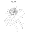
- FIG. 13 is a diagram showing a portion of the optical pickup device according to the embodiment of the invention.
- FIGS. 14 a , 14 b , 14 c , 14 d , 14 e , and 14 f are diagrams showing light which is emitted from a light source of the optical pickup device according to the embodiment of the invention.
- FIGS. 15 a and 15 b are diagrams showing light which is emitted from the light source of the optical pickup device according to the embodiment of the invention.
- FIG. 16 is a diagram showing a portion of the optical pickup device according to the embodiment of the invention.
- FIGS. 17 a , 17 b and 17 c are diagrams showing a portion of the optical pickup device according to the embodiment of the invention.
- FIGS. 18 a , 18 b , 18 c , and 18 d are diagrams showing a portion of the optical pickup device according to the embodiment of the invention.
- FIG. 19 is a diagram showing a portion of the optical pickup device according to the embodiment of the invention.
- FIG. 20 is a diagram showing a portion of the optical pickup device according to the embodiment of the invention.
- FIG. 21 is a diagram showing a portion of the optical pickup device according to the embodiment of the invention.
- FIG. 22 is a diagram showing a portion of the optical pickup device according to the embodiment of the invention.
- FIG. 23 is a diagram showing a portion of the optical pickup device according to the embodiment of the invention.
- FIG. 24 is a diagram showing a portion of the optical pickup device according to the embodiment of the invention.
- FIG. 25 is a diagram showing a portion of the optical pickup device according to the embodiment of the invention.
- FIG. 26 is a diagram showing a portion of the optical pickup device according to the embodiment of the invention.
- FIG. 27 is a diagram showing a portion of the optical pickup device according to the embodiment of the invention.
- FIG. 28 is a diagram showing a portion of the optical pickup device according to the embodiment of the invention.
- FIG. 29 is a diagram showing a portion of the optical pickup device according to the embodiment of the invention.
- FIG. 30 is a diagram showing a portion of the optical pickup device according to the embodiment of the invention.
- FIG. 31 is a diagram showing the temperature distribution of the optical pickup device according to the embodiment of the invention.
- FIG. 32 is a diagram showing a portion of the optical pickup device according to the embodiment of the invention.
- FIG. 33 is a diagram showing a portion of the optical pickup device according to the embodiment of the invention.
- FIG. 34 is a diagram showing a portion of the optical pickup device according to the embodiment of the invention.
- FIG. 35 is a diagram showing a portion of the optical pickup device according to the embodiment of the invention.
- FIG. 36 is a diagram showing a portion of the optical pickup device according to the embodiment of the invention.
- FIG. 37 is a diagram showing a portion of the optical pickup device according to the embodiment of the invention.
- FIG. 38 is a diagram showing a portion of the optical pickup device according to the embodiment of the invention.
- FIG. 39 is a diagram showing a portion of the optical pickup device according to the embodiment of the invention.
- FIG. 40 is a diagram showing a portion of the optical pickup device according to the embodiment of the invention.
- FIG. 41 is a diagram showing a portion of the optical pickup device according to the embodiment of the invention.
- FIG. 42 is a diagram showing a portion of the optical pickup device according to the embodiment of the invention.
- FIG. 43 is a diagram showing a portion of the optical pickup device according to the embodiment of the invention.
- FIG. 44 is a diagram showing a portion of the optical pickup device according to the embodiment of the invention.
- FIG. 45 is a diagram showing a portion of the optical pickup device according to the embodiment of the invention.
- FIG. 46 is a diagram showing a portion of the optical pickup device according to the embodiment of the invention.
- FIG. 47 is a diagram showing a portion of the optical pickup device according to the embodiment of the invention.
- FIG. 48 is a diagram showing a portion of the optical pickup device according to the embodiment of the invention.
- FIG. 49 is a diagram showing a portion of the optical pickup device according to the embodiment of the invention.
- FIG. 50 is a diagram showing a portion of the optical pickup device according to the embodiment of the invention.
- FIGS. 51 a and 51 b are diagrams showing a portion of the optical pickup device according to the embodiment of the invention.
- FIGS. 52 a and 52 b are diagrams showing a portion of the optical pickup device according to the embodiment of the invention.
- FIG. 53 is a diagram showing a portion of the optical pickup device according to the embodiment of the invention.
- FIGS. 54 a and 54 b are diagrams showing a portion of the optical pickup device according to the embodiment of the invention.
- FIGS. 55 a and 55 b are diagrams showing a portion of the optical pickup device according to the embodiment of the invention.
- FIGS. 56 a and 56 b are diagrams showing a portion of the optical pickup device according to the embodiment of the invention.
- FIGS. 57 a and 57 b are diagrams showing a portion of the optical pickup device according to the embodiment of the invention.
- FIGS. 58 a and 58 b are diagrams showing a portion of the optical pickup device according to the embodiment of the invention.
- FIGS. 59 a and 59 b are diagrams showing a portion of the optical pickup device according to the embodiment of the invention.
- FIG. 60 is a diagram showing an optical disk drive according to an embodiment of the invention.
- FIG. 61 is a diagram showing a portion of the optical disk drive according to the embodiment of the invention.
- FIG. 62 is a diagram showing a portion of the optical pickup device according to the embodiment of the invention.
- FIG. 63 is a diagram showing a portion of the optical pickup device according to the embodiment of the invention.
- FIG. 64 is a diagram showing a portion of the optical pickup device according to the embodiment of the invention.
- FIG. 65 is a diagram showing a portion of the optical pickup device according to the embodiment of the invention.
- FIG. 66 is a diagram showing a portion of the optical pickup device according to the embodiment of the invention.
- FIG. 67 is a diagram showing a portion of the optical pickup device according to the embodiment of the invention.
- FIG. 68 is a diagram showing a portion of the optical pickup device according to the embodiment of the invention.
- FIG. 69 is a diagram showing a portion of the optical pickup device according to the embodiment of the invention.
- FIG. 70 is a diagram showing a portion of the optical pickup device according to the embodiment of the invention.
- FIG. 71 is a diagram showing a portion of the optical pickup device according to the embodiment of the invention.
- FIG. 72 is a diagram showing a portion of the optical pickup device according to the embodiment of the invention.
- FIG. 73 is a diagram showing a portion of the optical pickup device according to the embodiment of the invention.
- FIG. 74 is a diagram showing a portion of the optical pickup device according to the embodiment of the invention.
- FIG. 1 is a schematic view illustrating the construction of an optical pickup device according to an embodiment of the present invention.
- the A-side of FIG. 1 from a short wavelength optical unit 1 and a long wavelength optical unit 3 to a collimator lens 8 by reference to a double wavy line is a schematic view when the optical pickup device is seen from a Z-direction (the top side of the page) in FIG. 2 .
- the B-side of FIG. 1 from a inclined-right mirror 9 to an optical disk 2 by reference to the double wavy line is a schematic view when the optical pickup device is seen from an R-direction in FIG. 2 .
- reference numeral 1 represents a short wavelength optical unit which emits short-wavelength laser.
- the short wavelength optical unit 1 emits light with a wavelength of 400 to 415 nm.
- the short wavelength optical unit 1 is constructed so as to emit light with a wavelength of 405 nm.
- light with the above-described laser wavelength has a blue color to violet color.
- the short wavelength optical unit 1 includes a light source section 1 a which emits short-wavelength laser, a light receiving section 1 b for detecting a signal which receives light reflected from the optical disk 2 , a light receiving section 1 c which is provided so as to monitor an amount of light emitted from the light source section 1 a , an optical member 1 d , and a holding member (not shown) which holds the above-described constituent members in a predetermined positional relationship.
- the light source member 1 a is provided with a semiconductor laser element (not shown) which consists primarily of GaN.
- the light emitted from the semiconductor laser element is incident on the optical member 1 d , and some of the incident light is reflected by the optical member 1 d so as to enter the light receiving section 1 c .
- the light receiving section 1 c is provided with a circuit which converts light into an electrical signal and adjusts the intensity of light to a desired level, the light being emitted from the light source section 1 a based on the electrical signal. Further, most of light emitted from the light source section 1 a is introduced toward the optical disk 2 through the optical member 1 d , and the light reflected from the optical disk 2 is incident on the light receiving section 1 b through the optical member 1 d .
- the light receiving section 1 b converts light into an electrical signal and generates an RF signal, a tracking error signal, a focus error signal and the like from the electrical signal.
- a hologram 1 e is provided to separate the reflected light from the optical disk 2 such that a focus error signal can be obtained.
- one short wavelength optical unit including the light source section 1 a , the light receiving sections 1 b and 1 c , and the optical member 1 d is constructed so as to miniaturize the optical pickup device.
- at least one of the receiving sections 1 b and 1 c may be removed from the short wavelength optical unit 1 so as to be separately constructed.
- the optical member 1 d may be removed from the short wavelength optical unit 1 so as to be separately constructed.
- Reference numeral 3 represents a long wavelength optical unit which emits laser with a long wavelength.
- the long wavelength optical unit 3 emitting light with a wavelength of 640 to 800 nm is constructed so as to emit light with one kind of wavelength or a plurality of lights with plural kinds of wavelengths.
- the long wavelength optical unit 3 is constructed so as to emit a light flux with a wavelength of about 660 nm (red: corresponding to DVD) and a light flux with a wavelength of about 780 nm (infrared: corresponding to CD).
- the long wavelength optical unit 3 includes a light source section 3 a which emits laser with a long wavelength, a light receiving section 3 b for detecting a signal which receives light reflected from the optical disk 2 , a light receiving section 3 c which is provided so as to monitor an amount of light emitted from the light source section 3 a , an optical member 3 d , a holding member (not shown) which holds those constituent members in a predetermined positional relationship.
- the light source section 3 a is provided with a semiconductor laser element (not shown).
- the semiconductor laser element is composed of a mono block (monolithic structure).
- the semiconductor layer element emits a light flux with a wavelength of about 660 nm (red) and a light flux with a wavelength of about 780 nm (infrared) from the mono-block element.
- the mono-block element emits two-light fluxes.
- two elements may be built therein, each element emitting one light flux.
- a plurality of light fluxes emitted from the semiconductor layer element are incident on the optical member 3 d , and some of the incident light is reflected by the optical member 3 d so as to enter the light receiving section 3 c .
- the light receiving section 3 c is provided with a circuit which converts light into an electrical signal and adjusts the intensity of light to a desired level, the light being emitted from the light source section 3 a based on the electrical signal. Further, most of light emitted from the light source section 3 a is introduced toward the optical disk 2 through the optical member 3 d , and the light reflected from the optical disk 2 is incident on the light receiving section 3 b through the optical member 3 d .
- the light receiving section 3 b converts light into an electrical signal and generates an RF signal, a tracking error signal, a focus error signal and the like from the electrical signal.
- the optical member 3 d is provided with a hologram 3 e which separates reflected light from the optical disk 2 into a plurality of lights such that the respective lights are guided to predetermined places of the light receiving section 3 b.
- one long wavelength optical unit including the light source section 3 a , the light receiving sections 3 b and 3 c , and the optical member 3 d is constructed so as to miniaturize the optical pickup device.
- at least one of the receiving sections 3 b and 3 c may be removed from the long wavelength optical unit 3 so as to be separately constructed.
- the optical member 3 d may be removed from the long wavelength optical unit 3 so as to be separately constructed.
- Reference numeral 4 represents a beam shaping lens, through which light emitted from the short wavelength optical unit 1 and reflected light from the optical disk 2 pass.
- the beam shaping lens 4 is formed of glass which is hardly degraded by the passing of short-wavelength laser.
- the beam shaping lens 4 may be formed of another material as long as the material is hardly degraded by the passing of short-wavelength laser.
- the beam shaping lens 4 is provided so as to remove astigmatism of short-wavelength laser and astigmatism occurring in a light path from the short wavelength optical unit 1 to the optical disk 2 .
- the light reflected from the optical disk 2 may be caused to be incident on the short wavelength optical unit 1 without the beam shaping lens 4 .
- the reflected light from the optical disk 2 is caused to be incident on the short wavelength optical unit 1 through the beam shaping lens 4 .
- the beam shaping lens 4 is used so as to reduce astigmatism of light with a short wavelength, a beam shaping prism or beam shaping hologram may be used instead.
- a convex portion 4 a and a concave portion 4 b are respectively provided.
- the beam shaping lens 4 is disposed so that the light emitted from the short wavelength optical unit 1 is first incident on the convex portion 4 a so as to be emitted from the concave portion 4 b.
- Reference numeral 5 represents an optical part.
- the optical part 5 is disposed ahead of the beam shaping lens 4 on the light path and in the side of the concave section 4 b of the beam shaping lens 4 . That is, the light emitted from the short wavelength optical unit 1 is incident on the optical part 5 through the beam shaping lens 4 so as to be guided to the optical disk 2 , and the light reflected from the optical disk 2 is incident on the short wavelength optical unit 1 after sequentially passing through the optical part 5 and the beam shaping lens 4 .
- the optical part 5 is provided with a hologram or the like, which has at least the following function. That is, the function is to separate the light reflected from the optical disk 2 into predetermined light fluxes so as to mainly generate a tracking error signal.
- the light is separated into a plurality of light fluxes by the hologram 1 e provided in the optical member 1 d , in order to generate a focus error signal. Further, the light is separated into a plurality of light fluxes by the optical part 5 , in order to generate a tracking error signal.
- the optical parts 5 may have a function of serving as a RIM intensity correction filter which attenuates the light intensity of short-wavelength light at the substantial center portion. Further, the optical parts 5 may be separated into two optical parts. One of the optical parts 5 can serve to separate the light reflected from the optical disk 2 into predetermined light fluxes so as to mainly generate a tracking error signal, and the other of the optical parts 5 can serve as a RIM intensity correction filter.
- Reference numeral 6 represents a relay lens though which long-wavelength light emitted from the long wavelength optical unit 3 passes.
- the relay lens 6 is formed of a transparent member such as resin or glass.
- the relay lens 6 is provided so as to effectively guide light emitted from the long wavelength optical unit 3 into a backward member. Further, with the relay lens 6 being provided, the long wavelength optical unit 3 can be disposed toward a beam splitter 7 , which makes it possible to realize the miniaturization of device.
- Reference numeral 7 represents a beam splitter.
- the beam splitter 7 at least two transparent members 7 b and 7 c are provided so as to be bonded to each other. Between the transparent members 7 b and 7 c , one inclined surface 7 a is provided on which a wavelength selecting film is formed. As the wavelength selecting film is directly formed on the inclined surface 7 a of the transparent member 7 c into which the light emitted from the short wavelength optical unit 1 enters, the transparent member 7 b is bonded to the inclined surface 7 a of the transparent member 7 c , on which the wavelength selecting film is formed, through a bonding material such as resin or glass.
- the beam splitter 7 has a function of reflecting the short-wavelength light emitted from the short wavelength optical unit 1 and transmitting the light emitted from the long wavelength optical unit 3 . That is, the light emitted from the short wavelength optical unit 1 and the light emitted from the long wavelength optical unit 3 are guided in the substantially same direction.
- Reference numeral 8 represents a collimator lens which is movably held.
- the collimator lens 8 is attached to a slider 8 b , and the slider 8 b is movably attached to a pair of support members 8 a which are provided substantially parallel to each other.
- a lead screw 8 c provided with a helical groove is provided substantially parallel to the support member 8 a , and a projection inserted into the groove of the lead screw 8 c is provided on the end portion of the slider 8 b .
- the lead screw 8 c is coupled to a gear group 8 d which is provided with a driving member 8 e .
- a driving force of the driving member 8 e is transmitted to the lead screw 8 c through the gear group 8 d , and the lead screw 8 c is rotated by the driving force.
- the slider 8 b moves along the support member 8 a . That is, the collimator lens 8 can be moved in a direction approaching or departing from the beam splitter 7 by a difference in driving direction or driving speed of driving member 8 e . Further, the speed of the movement can be adjusted.
- the driving member 8 e various motors are used, among which a stepping motor is preferably used.
- An amount of rotation of the lead screw 8 c is determined by adjusting the number of pulses to be sent to the stepping motor. As a result, it is possible to easily set an amount of movement of the collimator lens 8 .
- the collimator lens 8 is constructed so as to approach or depart from the beam splitter 7 , it is possible to easily adjust a spherical aberration. That is, the spherical aberration of short-wavelength light can be adjusted by the position of the collimator lens 8 . Therefore, at least any one of recording and reproducing can be effectively performed on a first recording layer provided in the optical disk, the first recording layer corresponding to a short wavelength, and a second recoding layer provided at a depth different from the first recording layer, respectively.
- the collimator lens 8 Through the collimator lens 8 , long-wavelength and short-wavelength lights incident from the beam splitter 7 pass. Therefore, the collimator lens 8 is formed of glass or, preferably, short-wavelength-light-resistant resin (which is not or hardly degraded by short-wavelength light). The collimator lens 8 transmits short-wavelength or long-wavelength light reflected by the optical disk 2 .
- the collimator lens 8 is moved by the driving member 8 e in order to correct a spherical aberration of short-wavelength light.
- the collimator lens 8 may be moved by another constituent member.
- the spherical aberration of short-wavelength light may be adjusted by another unit.
- Reference numeral 9 represents a inclined-right mirror.
- the inclined-right mirror 9 is provided with a quarter wavelength member 9 a acting on short-wavelength light.
- a quarter wavelength member is preferably used, which can rotate a polarization direction of light at about 90 degrees, the light having passed two times (through an outward path and inward path).
- the quarter wavelength member 9 a is interposed inside the inclined-right mirror 9 .
- a wavelength selecting film 9 b is provided, which has a function of reflecting most of long-wavelength light emitted from the long wavelength optical unit 3 and transmitting most of short-wavelength light emitted from the short wavelength optical unit 1 .
- Reference numeral 10 represents an object lens for long-wavelength laser.
- the object lens 10 condenses light reflected from the inclined-right mirror 9 on the optical disk 2 .
- the object lens 10 is used in this embodiment, other condensing members such as a hologram and the like may be used. Further, it is natural that the light reflected from the optical disk 2 passes through the object lens 10 .
- the object lens 10 is formed of glass or resin.
- Reference numeral 11 represents an optical part.
- the optical part 11 is an optical part provided between the object lens 10 and the inclined-right mirror 9 .
- the optical part 11 includes an aperture filter for implementing a required number of apertures which can correspond to a DVD optical disk (light with a wavelength of about 660 nm) and a CD optical disk (light with a wavelength of about 780 nm); a polarization hologram responding to light with a wavelength of about 660 nm; and a quarter wavelength member (preferably, a quarter wavelength plate).
- the optical part 11 is composed of a dielectric multilayer, a diffraction grating aperture unit or the like.
- the polarization hologram adds polarized light to light with a wavelength of about 660 nm (light with a wavelength of about 660 nm is separated into light for tracking error signal or focus error signal). Further, the quarter wavelength member rotates the polarization direction of an inward path of light with a wavelength of about 660 nm or 780 nm with respect to an outward path thereof, by 90 degrees.
- Reference numeral 12 represents a inclined-right mirror which reflects most of short-wavelength light.
- the inclined-right mirror 12 is provided with a reflective film.
- Reference numeral 13 represents an object lens.
- the object lens 13 condenses light reflected from the inclined-right mirror 12 on the optical disk 2 .
- the object lens 13 is used in this embodiment, other condensing members such as a hologram and the like may be used. Further, it is natural that the light reflected from the optical disk 2 passes through the object lens 13 .
- the object lens 13 is formed of glass or resin. In this case, when the object lens 13 is formed of resin, it is preferable that the object lens 13 is formed of short-wavelength-light-resistant resin (which is not or hardly degraded by short wavelength light).
- Reference numeral 14 represents an achromatic diffraction lens provided between the object lens 13 and the inclined-right mirror 12 .
- the achromatic diffraction lens 14 has a function of correcting a chromatic aberration.
- the achromatic diffraction lens 14 is provided so as to reduce a chromatic aberration occurring in each optical part through which short-wavelength light passes.
- the achromatic diffraction lens 14 is constructed by forming a desired hologram on a lens, and the correction degree of chromatic aberration can be determined by adjusting at least one of a grating pitch of the hologram and the curvature radius of the lens.
- the achromatic lens 14 is formed of resin such as plastic or glass. When resin is used, it is preferable that the achromatic lens 14 is formed of short-wavelength-light-resistant resin (which is not or hardly degraded by short wavelength light).
- FIG. 2 illustrates an example where the optical construction shown in FIG. 1 is embodied. Although members thereof have a slightly different shape from the respective members shown in FIG. 1 , functions thereof are the substantially same.
- Reference numeral 15 represent a base. On the base 15 , the above-described respective members are fixed or movably attached.
- the base 15 is formed of metal or metallic alloy, such as zinc, a zinc alloy, aluminum, an aluminum alloy, titanium, a titanium alloy or the like.
- the base 15 is manufactured using a die casting method in terms of mass production.
- the base 15 is movably held by a pickup module shown in FIGS. 3 and 4 .
- Reference numeral 20 represents a frame.
- the frame 20 has shafts 21 and 22 disposed in parallel to each other.
- the base 15 is movably attached to the shafts 21 and 22 .
- a screw shaft 23 provided with a helical groove is attached substantially parallel to the shafts 21 and 22 so as to freely rotate around the frame 20 .
- a member provided integrally with or separately from the base 15 is geared into the groove provided on the screw shaft 23 .
- the screw shaft 23 is geared with a gear group 24 a which is rotatably provided in the frame 20 , and the gear group 24 a is geared with a feed motor 24 .
- the gear group 24 a rotates.
- the screw shaft 23 is rotated.
- the base 15 can reciprocate in an arrow direction shown in FIG. 3 .
- the feed motor 24 is disposed substantially parallel to the screw shaft 23 .
- the frame 20 has the optical disk 2 mounted thereon, and a spindle motor 25 for rotating the optical disk 2 is attached by such a technique as screw fastening or bonding.
- a control board 26 is provided separately from the frame 20 , as shown in FIG. 3 .
- the control board 26 and the base 15 are electrically coupled through a flexible board 29 , and the control board 26 is also electrically connected to the spindle motor 25 by a member which is not shown.
- the control board 26 is provided with a connector 27 which performs electric connection with the control board provided in the optical disk drive.
- a flexible board (not shown) or the like is plugged in the connector 27 , thereby performing electrical connection.
- a frame cover 30 having a function of protecting members may be provided at least in the side of the frame 20 opposite to the optical disk.
- the frame cover 30 is provided with a through-hole 31 , from which at least the object lenses 10 and 13 are exposed in the base 15 and the spindle motor 25 projects by a predetermined amount.
- the frame 20 is provided with an attachment section 20 a for fixing the frame 20 to another member, and a screw or the like is inserted into the attachment section 20 a so as to attach the frame 20 to another member.
- the short wavelength optical unit 1 , the long wavelength optical unit 3 , the beam shaping lens 4 , the optical part 5 , the relay lens 6 , the beam splitter 7 , the support member 8 a , the lead screw 8 c , the gear group 8 d , the driving member 8 e , the inclined-right mirrors 9 and 12 and the like are bonded to the base 15 by using an organic adhesive such as a light-curing adhesive or epoxy-based adhesive or a metallic adhesive such as solder or lead-free solder. Alternately, they are attached to the base 15 by a technique such as screw fastening, fitting, pressing-in or the like.
- the lead screw 8 c and the gear group 8 d are rotatably attached to the base 15 .
- Reference numeral 17 represents a suspension holder.
- the suspension holder 17 is attached to the base 15 by various bonding techniques through a yoke member to be described below.
- the lens holder 16 and the suspension holder 17 are coupled to each other through a plurality of suspensions 18 .
- the lens holder 16 is supported so as to move in a predetermined range with respect to the base 15 .
- the object lens 10 and 13 , the optical part 11 , the achromatic diffraction lens 14 and the like are attached to the lens holder 16 . In accordance with the movement of the lens holder 16 , the object lens 10 and 13 , the optical part 11 , the achromatic diffraction lens 14 and the like are moved together with the lens holder 16 . As shown in FIG.
- the inclined-right mirrors 9 and 12 are attached to protuberating portions 15 d and 15 e , respectively, by a light-curing resin or instant adhesive, the protuberating portions 15 d and 15 e being provided so as to protuberate on the base 15 .
- a bonding position between the inclined-right mirror 9 and the protuberating portion 15 d is considered so as not to block light passing through the inclined-right mirror 9 . Since the inclined-right mirrors 9 and 12 are provided so as to be positioned under the lens holder 16 , they are not shown in FIG. 2 .
- the inclined-right mirror 9 is provided to be inclined with respect to the light flux which is emitted from the short wavelength optical unit 1 so as to pass through the beam splitter 7 and the collimator lens 8 . Therefore, the light flux coming from the short wavelength optical unit 1 is refracted when passing through the inclined-right mirror 9 . Then, the light flux moves in a direction away from the object lenses 10 and 13 by a distance d shown in FIG. 5 .
- the object lenses 10 and 13 are disposed in an order of the object lens 10 and the object lens 13 along the direction where light emitted from the short wavelength optical unit 1 or long wavelength optical unit 3 so as to pass through the beam splitter 7 or the collimator lens 8 proceeds.
- the thickness of the object lens 13 on the lens axis is larger than that of the object lens 10 .
- the object lenses 10 and 13 are disposed in an order of the object lens 13 and the object lens 10 from the side of the suspension holder 17 , as shown in FIG. 6 .
- the object lenses 10 and 13 are disposed in such a manner, a light flux is not blocked by the object lens 13 or the achromatic diffraction lens 14 even though the lens holder 16 is driven up and down. Therefore, it is possible to make the optical pickup device slim.
- FIG. 7 is a sectional view taken along A-A line of FIG. 6 showing the optical pickup device according to this embodiment.
- the lens holder 16 is provided with through-holes 16 a and 16 b .
- the object lenses 10 and 13 are brought down into the through-holes 16 a and 16 b , respectively, from a direction of an arrow P 1 shown in FIG. 7 and are then fixed by a light-curing adhesive or the like.
- the outer circumferences of the object lenses 10 and 13 are abutted on the circumferential edges of the through-holes 16 and 16 b of the lens holder 16 , respectively.
- the optical part 11 and the achromatic lens 14 are inserted into the through-holes 16 a and 16 b , respectively, from a direction of an arrow P 2 shown in FIG.
- Reference numerals 33 and 34 represent a focus coil. As shown in FIG. 6 , the respective focus coils 33 and 34 are wound in a substantial ring shape and are provided in diagonal positions of the lens holder 16 . Reference numerals 35 and 36 , respectively, represent a tracking coil. The respective tracking coils 35 and 36 are also wound in a substantial ring shape and are provided in different diagonal positions of the lens holder 16 . Between the focus coils 33 and 34 and the lens holder 16 , sub-tracking coils 37 and 38 are respectively provided. With the sub-tracking coils 37 and 38 being provided, it is possible to suppress unnecessary inclination of the lens holder occurring on tracking.
- the sub-tracking coils 37 and 38 are bonded to the lens holder 16 by an organic adhesive such as a heat-curing adhesive or the like. Then, the focus coils 33 and 34 may be bonded on the sub-tacking coils 37 and 38 by an adhesive or the like. Further, a bonding body in which the sub-tracking coil 37 and the focus coil 33 are previously bonded may be bonded to the lens holder 16 .
- a heat-curing adhesive is used for bonding between the coils and the lens holder 16 or bonding between the coils.
- a light-curing adhesive or other adhesives may be used for bonding. Further, if the coils and the lens holder or the coils can be reliably disposed in predetermined positions, other methods may be used for bonding.
- Three of the suspensions 18 are provided in each side of the lens holder such that the lens holder 16 is interposed therebetween.
- the suspensions 18 elastically connect the suspension holder 17 and the lens holder 16 .
- At least the lens holder 16 can be displaced in a predetermined range with respect to the suspension holder 17 .
- three of suspensions 18 are provided in one side (six in total), a larger number (for example, eight) of suspensions 18 may be provided, or a smaller number (for example, four) of suspensions 18 may be provided.
- suspensions 18 a , 18 b , and 18 c are respectively set to suspensions 18 a , 18 b , and 18 c from the side opposite to the optical disk 2
- three of the suspensions 18 positioned in the lower side of FIG. 6 are respectively set to suspensions 18 d , 18 e , and 18 f from the side opposite to the optical disk 2 .
- Both ends of the suspension 18 are fixed to the lens holder 16 and the suspension holder 17 , respectively, by insert molding.
- Both ends of the focus coil 33 are electrically connected to the suspensions 18 a and 18 b , respectively, and both ends of the focus coil 34 are electrically connected to the suspensions 18 d and 18 e , respectively. Further, the tracking coil 35 , the sub-tracking coil 37 , tracking coil 36 , and the sub-tracking coil 38 are connected in series. One end of the coil group connected in series is connected to the suspension 18 c , and the other end of the coil group is connected to the suspension 18 f . The ends of the respective coils and the suspensions 18 are electrically connected by a metallic bonding material such as solder or lead-free solder.
- the suspensions 18 may be composed of wire of which the cross-section is formed in a substantially circular or elliptical shape or in a polygonal shape such as a rectangle. Further, a plate spring may be processed into the suspension 18 .
- the suspension 18 is formed in a reverse V-shape, if it is seen from the light emission direction of the object lenses 10 and 13 with the suspension holder 17 being set in the lower side. In the suspension 18 , tension is applied. Accordingly, it is possible to reduce the size and the resonance of the suspension 18 in a buckling direction.
- Reference numeral 32 represents a yoke member formed of Fe or a Fe alloy. If Fe or a Fe alloy is used, it is easy to construct a magnetic circuit.
- the yoke member 32 is integrally provided with upright portions 32 a , 32 b , and 32 c facing the respective coils provided in the lens holder 16 by a cutting and raising process. Further, on the lower surface of the yoke member 32 , an opening portion 32 d is provided. From the opening portion 32 d , the inclined-right mirrors 9 and 12 fixed to the base 15 enter. Further, the suspension holder 17 is fixed on the yoke member 32 by a technique such as bonding, and the yoke member 32 is bonded to the base 15 by a technique such as bonding.
- Reference numerals 39 to 42 are magnets provided on the yoke member 32 by a technique such as bonding or the like.
- the magnet 39 is attached to the upright portion 32 c and is provided so as to face the focus coil 33 and the sub-tracking coil 37 . Further, the magnet 39 is disposed in the yoke member 32 and is magnetized so that a magnetic pole thereof is exposed on the surface facing the focus coil 33 and the sub-tracking coil 37 in an order of the S pole and the N pole in the height direction of FIG. 7 from the bottom surface toward the object lenses 10 and 13 .
- the magnet 40 is attached in the side opposite to the side, where the magnet 39 of the upright portion 32 c is attached, in the width direction shown in FIG. 6 . Further, the magnet 40 is provided so as to face the tracking coil 35 .
- the upright portion 32 c is widely formed in the width direction shown in FIG. 6 , in order to increase rigidity of the yoke member 32 .
- the upright portion 32 c may be divided into two portions such that the magnet 39 is attached to one of them by bonding or the like and the magnet 40 is attached to the other.
- the magnet 40 is disposed in the yoke member 32 and is magnetized so that a magnetic pole thereof is exposed on the surface facing the tracking coil 35 in an order of the N pole and the S pole from the inside in the width direction shown in FIG. 6 .
- the magnet 41 is attached on the upright portion 32 b and is provided so as to face the tracking coil 36 . Further, the magnet 41 is disposed in the yoke member 32 and is magnetized so that a magnetic pole thereof is exposed on the surface facing the tracking coil 36 in an order of the N pole and the S pole from the inside in the width direction shown in FIG. 6 .
- the magnet 42 is attached on the upright portion 32 a and is provided so as to face the focus coil 34 and the sub-tracking coil 38 . Further, the magnet 42 is disposed in the yoke member 32 and is magnetized so that a magnetic pole thereof is exposed on the surface facing the focus coil 34 and the sub-tracking coil 38 in an order of the S pole and the N pole in the height direction of FIG. 7 from the bottom surface toward the object lenses 10 and 13 .
- FIG. 9 clearly shows a dispositional relationship between the respective sections
- FIG. 10 is a sectional view of the short wavelength optical unit 1 .
- At least the light source section 1 a , the light receiving sections 1 b and 1 c , and the optical member 1 d are directly or indirectly attached to a loading section 43 . Further, the back end of the loading section 43 is attached to a holding member 44 .
- the attachment portion 43 c of the loading section 43 with respect to the holding member 44 is formed in a convexly curved shape, and similarly, the attachment portion of the holding member 44 with respect to the loading section 43 is formed in a concavely curved shape.
- the loading section 43 is combined with the holding member 44 . Further, as the curved-shaped portions thereof are moved so as to slide, the loading section 43 and the holding member 44 are positioned in a desired positional relationship. After that, the loading section 43 and the holding member 44 are fixed to each other by a metallic adhesive such as solder or an organic adhesive.
- the loading section 43 is provided with a light source housing section 43 a which can house at least a portion of the light source section 1 a . After being housed in the light source housing section 43 a , the light source section 1 a is bonded by a bonding material so as not to be detached from the light source housing section 43 a . Further, a through-hole 43 b is provided in a portion facing the light-emitting portion of the light source section 1 a so as to communicate with the light source housing section 43 a . The light emitted from the light source section 1 a passes through the through-hole 43 b so as to be guided to the optical member 1 d .
- the optical member 1 d includes at least an optical section 46 having an inclined surface 46 a and an optical section 47 having a plurality of inclined surfaces formed therein.
- the loading section 43 has a light receiving section attaching portion 48 integrally formed, the light receiving section attaching portion 48 facing the optical member 1 d .
- the light receiving section attaching portion 48 is provided with a through-hole 45 .
- the light receiving section 1 b is attached through a flexible printed board 49 by a technique such as bonding. Although the flexible printed board 49 is omitted and is shown in FIG.
- the flexible printed board 49 electrically connects the light receiving section 1 b to another member and is provided with a through-hole 49 a .
- the light from the optical member 1 d is guided to the light receiving section 1 b through the through-holes 45 and 49 a .
- a light receiving section attaching portion 50 is integrally provided in the loading section 43 so as to face the light receiving section attaching portion 48 , and the optical member 1 d is disposed between the light receiving section attaching portions 48 and 50 .
- the light receiving section attaching portion 50 is provided with a through hole (not shown), and the light receiving section 1 c is attached to the light receiving section attaching portion 50 by a technique such as bonding.
- the light from the optical section 46 passes through the through-hole of the light receiving attaching portion 50 (not shown) so as to be incident on the light receiving section 1 c.
- optical sections 46 and 47 of the optical member 1 d will be described in detail with reference to FIG. 11 .
- the short-wavelength light emitted from the light-emitting point of the light source section 1 a is guided to the optical section 46 through a cover glass 51 provided in a portion serving as a light-emission window of the light source section 1 a .
- the light incident on a plane 46 b provided substantially parallel to the cover glass 51 of the optical section 46 passes through the optical section 46 , and the light incident on the inclined surface 46 a inclined to the plane 46 b is reflected so as to be incident on the light receiving section 1 c (which is not shown in FIG. 11 ).
- the lights are used for monitoring an optical output.
- a reflecting section is formed of a dielectric multilayer or metallic film.
- the plane 46 c has a dimming filter (not shown) formed thereon, and light dimmed by the dimming filter is guided to the optical section 47 .
- the dimming filter has various transmittances, the transmittance thereof is adjusted by a spread angle of light emitted from the light source section 1 a . That is, when a spread angle of light from the light source section 1 a is large, the transmittance of the dimming filter becomes small. Alternately, when a spread angle of light from the light source section 1 a is small, the transmittance of the dimming filter becomes large.
- the transmittance of the dimming filter is adjusted by a spread angle of light from the light source section 1 a , it is possible to prevent undesired occurrence of data erasing which is caused by excessively intensive light output when recording or reproducing is performed on a single-layer disk or multi-layer disk.
- a spread angle of light emitted from the light source section 1 a is previously classified into predetermined ranges.
- a dimming filter having a different transmittance is provided in each of the classified light source sections 1 a , thereby obtaining an excellent recording/reproducing characteristic with respect to an optical disk.
- the dimming filter is formed of a dielectric multilayer film or metallic film. When transmittance is adjusted and a dielectric multilayer film is used, it is possible to adjust a constituent material or film construction thereof or a thickness thereof. When a metallic film is used, it is possible to adjust a constituent material or thickness thereof.
- the light passing through the plane 46 c is incident on the optical section 47 .
- the optical section 47 is formed in a rectangular parallelepiped shape as a whole.
- a light absorbing film having a function of absorbing light is provided except for a predetermined region.
- the light absorbing film prevents the light emitted from the light source section 1 a from being incident on the optical section 47 from a place excluding a predetermined portion. At least some of light, which is emitted from the light source 1 a so as to pass through the optical section 46 , is incident on the inside of the optical section 47 from a portion where the light absorbing film of the bottom surface 53 is not disposed.
- the optical section 47 is constructed by bonding blocks 58 to 61 formed of transparent glass or the like.
- An inclined surface 54 is formed on a bonding portion between the block 58 and the block 59 , an inclined surface 55 is formed between the block 59 and the block 60 , and an inclined surface 56 is formed between the block 60 and the block 61 .
- Inside the optical section 47 at least the inclined surfaces 54 , 55 , and 56 are provided, and the end portions of the inclined surfaces 54 , 55 , and 56 are exposed to the surface of the optical section 47 .
- the inclined surface 54 is provided with a first polarized beam splitter
- the inclined surface 55 is provided with a second polarized beam splitter.
- both of the first and second polarized beam splitters are directly formed in the block 59
- the first polarized beam splitter may be formed in the block 58 and the second polarized beam splitter may be formed in the block 60 .
- Both of the first and second polarized beam splitters have a function of transmitting p-polarization light (hereinafter, abbreviated to a p-wave) and reflecting s-polarization light (hereinafter abbreviated to an s-wave).
- at least the first and second polarized beam splitters may be provided in a portion within the optical section 47 through which light mainly passes. In this embodiment, however, the first and second polarized beam splitters are provided on the entire inclined surfaces 54 and 55 , in consideration of productivity.
- On the inclined surface 56 a reflective film and a hologram (the same as the hologram 1 e shown in FIG. 1 ) are formed, the hologram 57 generating astigmatism.
- the light passing through the bottom surface of the optical section 47 from the light source section 1 a so as to be incident on the optical section 47 is an s-wave.
- the light is reflected by the first polarized beam splitter provided on the inclined surface 54 so as to be incident on the second polarized beam splitter formed on the inclined surface 55 .
- the second polarized beam splitter also reflects an s-wave. Therefore, the light incident on the second polarized beam splitter is reflected so as to be emitted from the top surface 62 z of the optical section 47 and then passes through the above-described members so as to be guided to the optical disk 2 .
- the light reflected by the optical disk 2 is converted into a p-wave by the action of the quarter wavelength member 9 a and is again incident on the optical section 47 from the top surface 62 z of the optical section 47 .
- the portion where the light is emitted from the optical section 47 toward the optical disk 2 and the portion where the light reflected from the optical disk 2 is incident are located in the substantially same position. Since the light reflected by the optical disk 2 so as to return to the optical section 47 is a p-wave as described above, the light is transmitted through the second polarized beam splitter provided on the inclined surface 55 so as to be incident on the inclined surface 56 .
- the inclined surface 56 is provided with the reflective hologram 57 generating astigmatism, and the reflected light from the optical disk 2 is separated in predetermined directions by the hologram 57 such that a focus error signal can be obtained. Since the light reflected by the inclined surface 56 is a p-wave, the light is once again transmitted through the second polarized beam splitter and is then transmitted through the block 59 . Further, since the first polarized beam splitter also has a property of transmitting a p-wave as described above, the light is transmitted though the first polarized beam splitter and is then transmitted through the block 58 . Further, the light is emitted outside the optical section 47 and is then incident on the light receiving section 1 b.
- the light source section 1 a is composed of the following members.
- the light source section 1 a has a base 62 formed of a metallic material.
- a concave portion 62 a is provided which is used in adjusting the position of the light source section 1 a .
- through-holes 62 b and 62 c are provided.
- another through-hole is provided in addition to the through-holes 62 b and 62 c .
- the cover member 63 is bonded to the base 62 by welding or soldering, and a rectangular through-hole 64 is provided on the top surface of the cover member 63 on which a cover glass 65 (the same as the cover glass 51 of FIG. 11 ) is attached by bonding so as to block the through-hole 64 .
- the cross-section of the cover member 63 is formed in an elliptical or oval shape.
- a block 66 is provided which is formed of copper or a copper alloy having excellent heat conductivity.
- the block 66 is bonded to the base 62 by welding or a metallic bonding material.
- the cross-section of the block 66 is formed in a substantially semi-circular shape.
- a semiconductor laser element 68 is provided through a sub-mount 67 formed of a metallic material. Accordingly, the sub-mount 67 and the semiconductor laser element 68 as well as the block 66 are disposed within a region surrounded by the base 62 and the cover member 63 . Further, the light-emitting surface of the semiconductor laser element 68 is disposed so as to face the cover glass 65 , and light is emitted outside from the cover glass 65 . In the through-holes 62 b and 62 c and the other through-hole provided in the base 62 , rod-shaped terminals 69 , 70 , and 71 are respectively inserted.
- Portions of the terminals 69 , 70 , and 71 which are inserted into the through-holes 62 b and 62 c and the other through-hole, are attached to the base 62 though insulating materials such that the insulating between the base 62 and the terminals 69 , 70 , and 71 is secured.
- the leading end portions of the terminal 69 , 70 , and 71 are formed so as to project within the region surrounded by the base 62 and the cover member 63 .
- the terminal 69 and the sub-mount 67 are connected through gold wire 69 a , and the terminal 69 and the n-type GaN side of the semiconductor laser element 68 are electrically connected through the sub-mount 67 .
- terminal 70 and the p-type GaN side of the semiconductor laser element 68 are electrically connected through gold wire 70 a . Accordingly, electric power is supplied to the semiconductor laser element 68 through the terminals 69 , 70 , and 71 , thereby emitting short-wavelength light.
- the semiconductor laser element 68 it is preferable to use a GaN-based semiconductor laser element in which an active layer (gallium nitride with the emission center, such as In or the like) is provided between a p-type GaN layer and n-type GaN layer.
- the semiconductor layer element 68 emits light with a wavelength of 400 to 415 nm. It is natural to use a semiconductor laser element based on other materials, which emits different short-wavelength laser.
- the p-type GaN layer, the n-type GaN layer, and the active layer are laminated substantially parallel to a long-side direction X.
- a structure is used, in which the n-type GaN layer, the active layer, and the p-type GaN layer are sequentially laminated from the side of the sub-mount 67 .
- another structure may be used, in which the p-type GaN layer, the active layer, and the n-type GaN layer are sequentially laminated from the side of the sub-mount 67 .
- the laminated direction of the active layer of the semiconductor laser element 68 is not parallel to the long side 62 d of the base 62 (in this embodiment, the laminated direction perpendicularly crosses the long side 62 d ). Further, since the long side 62 d of the base 62 is attached to the base 15 so as to be perpendicular to the thickness direction of the base 15 , the active layer of the semiconductor laser element 68 is laminated substantially parallel to the thickness direction of the base 15 .
- the long side 62 d of the base 62 is attached so as to be substantially perpendicular to the thickness direction of the base 15 .
- the laminated direction of the semiconductor laser element 68 may be substantially parallel to the thickness direction of the base 15 .
- the long-side portion having a rectangular cross-section is bonded to the sub-mount 67 in the relationship between the base 62 and the semiconductor laser element 68 . Therefore, the long side 62 d of the base 62 is not parallel to the long-side direction X of the semiconductor laser element 68 (in this embodiment, the long-side direction X perpendicularly crosses the long side 62 d ). In such a construction, the cross-section of light discharged from the semiconductor laser element 68 can be discharged so that the long axis of the elliptical intensity distribution of emitted light is substantially parallel to the long side 62 d of the base 62 . As shown in FIG.
- reference numeral 72 represents an axis substantially parallel to the long side 62 d of the base 62
- reference numeral 74 is an outline of light in which the intensity distribution of light discharged from the semiconductor laser element 68 is indicated by a line where intensity becomes uniform
- reference numeral 73 represents a long axis of the elliptical outline 74 of discharged light.
- an angle ⁇ at which the axis 72 and the long axis 73 cross each other is not 90 degrees, as shown in FIG. 14A .
- the axis 72 and the long axis 73 cross each other at different angles, as shown in FIGS. 14B and 14C .
- the angle ⁇ is defined as the minimum angle among angles at which the axis 72 and the long axis 73 cross each other. That is, the angle ⁇ is more than 0 degree and less than 90 degrees.
- the axis 72 and the long axis 73 are parallel to each other, as shown in FIG. 14B , and the long axis 73 and the axis 72 cross each other at predetermined angles ⁇ , as shown in FIGS. 14B to 14F .
- the angle ⁇ at which the axis 72 and the long axis 72 cross each other is set to be in the range of 0 to 45 degrees. More preferably, the angle ⁇ is set to be in the range of 0 to 30 degrees.
- the angle ⁇ is set to be in the range of 0 to 10 degrees.
- the long axis 73 and the axis 72 become substantially parallel to each other (the angle ⁇ is almost 0 degree), as shown in FIG. 14B .
- the axis 72 is set to be parallel to the long side 62 d of the base 62 .
- the axis 72 can be also defined in the relationship with other constituent members, as follows. That is, the axis 72 can be defined as an axis which is parallel to the main surface of the mount optical disk 2 and is perpendicular to the direction of light emitted from the cover glass 65 of the light source section 1 a .
- the axis 72 can be defined as an axis which is perpendicular to the thickness direction of the base 15 shown in FIG. 2 and is also perpendicular to the direction of light emitted from the cover glass 65 of the light source section 1 a . Further, the axis 72 can be defined as an axis which is parallel to the bottom surface of the base 15 and is perpendicular to the direction of light emitted from the cover glass 65 of the light source section 1 a . Furthermore, the axis 72 can be defined as an axis which is perpendicular to the rotating shaft of the spindle motor 25 and is also perpendicular to the direction of light emitted from the cover glass 65 of the light source section 1 a.
- the long axis in the outline of light emitted from the light source section 1 a is set in such a positional relationship, it is possible to increase utilization efficiency of light. If the light source section 1 a having the same output is used, it is possible to irradiate light having a larger output onto the optical disk 2 . If the intensity of light irradiated on the optical disk 2 is set to the same magnitude, it is possible to use a light source section 1 a with a smaller output.
- FIG. 15A shows a case where the axis 72 and the long axis 73 perpendicularly cross each other, that is, a case where the outline is formed in a longitudinally-long elliptical shape.
- the light intensity of the center Q (point where the long axis and the short axis cross each other) of the outline 74 is set to 1, light of a region up to a portion having a predetermined proportion of light intensity in the direction along the axis 72 is used.
- the predetermined proportion is 0.6 (although the proportion is determined depending on a specification, it is typically in the range of 0.3 to 0.8), and the light of a circular region 75 , in which left and right distances from the center Q are set to L 1 and L 2 , can be used. That it, the light of the elliptical region 75 having a diameter of L 1 +L 2 can be used.
- L 1 is substantially equal to L 2 (L 1 ⁇ L 2 )
- a region of light to be substantially used becomes the circular region 75 with a radius of L 1 or L 2 .
- the outline is formed in a longitudinally-long elliptical shape.
- the distances L 1 and L 2 from the center Q to where a light intensity becomes 0.6 of the light intensity at the center Q become relatively small in the direction of the axis 72 , and a region with available light intensity is small.
- the predetermined proportion is 0.6 (although the proportion is determined depending on a specification, it is typically in the range of 0.3 to 0.8), and the light of a circular region 75 , in which left and right distances from the center Q are set to L 3 and L 4 , can be used. That it, the light of the circular region 75 having a diameter of L 3 +L 4 can be used.
- L 3 is substantially equal to L 4 (L 3 ⁇ L 4 )
- a region of light to be substantially used becomes the circular region 75 with a radius of L 3 or L 4 .
- the outline 74 is formed in a laterally-long elliptical shape. Therefore, the distances L 3 and L 4 from the center Q to where a light intensity becomes 0.6 of the light intensity at the center Q become relatively large in the direction of the axis 72 , and a region with available light intensity becomes much larger than in the example of FIG. 15A , which makes it possible to effectively use light. That is, the following relationship is established: L 1 ⁇ L 3 and L 2 ⁇ L 4 .
- the long axis 73 of elliptically-shaped light emitted from the light source section 1 a is set at a predetermined angle (including 0 degree) with respect to the axis 72 , as described above. Therefore, as the long side 62 of the base 62 is attached toward the base 15 as shown in FIGS. 12 and 13 , the long axis of the elliptically-shaped light emitted from the light source section 1 a can be set to be substantially parallel to the base 15 , and the height of the light source section 1 a does not become large. Accordingly, it is possible to make the device slim.
- the optical disk drive has a thickness of, preferably, less than 18 mm, or more preferably, less than 15 mm, or most preferably, less than 13 mm. Therefore, attaching the light source section 1 a at a low level can implement such an optical disk drive. Further, when the axis 72 and the long axis 73 are set at a predetermined angle (larger than 0 degree and less than 90 degrees), the following method is used in order to make the device slim.
- the light source section 1 a itself is rotated at a predetermined angle so as to be attached (in this case, when the light source section 1 a is attached, the attachment height becomes slightly large), the block 66 in the light source section 1 a is rotated by a predetermined amount so as to be attached to the base 62 , or the semiconductor laser element 68 is attached to the block 66 so as to be inclined to the long side 62 d.
- a loading section 76 is provided with a light source holding section 76 a .
- the light source 3 a is bonded to the light source holding section 76 a by a bonding material such as solder, lead-free solder, or light-curing resin.
- the optical member 3 d is attached on the light source holding section 76 a of the loading section 76 .
- the light receiving sections 3 b and 3 c are attached to the loading section 76 by a bonding material such as light-curing resin so as to interpose the optical member 3 d .
- the light source section 3 a covers at least a portion of a lead frame 77 through a molding member 78 such as resin, and a semiconductor laser element 79 is attached on the lead frame 77 to which terminals 77 a to 77 c are electrically connected.
- the semiconductor laser element 79 emitting light with a wavelength of 640 to 800 nm is constructed so as to emit light with one kind of wavelength or a plurality of lights with plural kinds of wavelengths.
- the semiconductor laser element 79 is constructed so as to emit a light flux with a wavelength of about 660 nm (red: corresponding to DVD) and a light flux with a wavelength of about 780 nm (infrared: corresponding to CD).
- the semiconductor laser element 79 as a mono-block element is constructed so as to emit two light fluxes.
- an element emitting one light flux as one block may be provided on the plurality of lead frames 77 .
- the optical member 3 d is composed of two optical sections 80 and 81 .
- the optical section 80 is formed in a plate shape.
- a film for coping with stray light is formed so that unnecessary light emitted from the light source section 3 a does not reach the optical section 81 . That is, the film for coping with stray light has an opening such that most of light is guided to the optical section 81 through the opening.
- the film is formed of such a material that absorbs light incident on a portion excluding the opening.
- a hologram having a wavelength selection property is provided, which acts on light corresponding to CD but hardly act on light corresponding to DVD. The hologram separates light corresponding to CD into three beams.
- the optical section 81 is provided on the optical section 80 and is formed by bonding blocks 82 to 85 made of transparent glass.
- An inclined surface 86 is formed in a bonding portion between the block 82 and the block 83
- an inclined surface 87 is between the block 83 and the block 84
- an inclined surface 88 is formed between the block 84 and the block 85 .
- Inside the optical section 81 at least the inclined surfaces 86 , 87 , and 88 are provided, and the end portions of the inclined surfaces 86 , 87 , and 88 are exposed to the surface of the optical section 81 .
- the inclined surface 86 has at least one of a reflective film and hologram provided in a transmitted portion of light such that 3 to 15% of light emitted from the light source section 3 a is reflected. Further, the inclined surface 86 has a dielectric multilayer formed thereon. The dielectric multilayer transmits a p-wave of light corresponding to CD and light corresponding to DVD and reflects an s-wave. The light reflected by the inclined surface 86 is incident on the light receiving section 3 c so as to be used for controlling an optical output of the light source section 3 a . Further, the inclined surface 87 has a dielectric multilayer formed thereon.
- the dielectric multilayer transmits a p-wave of light corresponding to CD and light corresponding to DVD, reflects an s-wave of light corresponding to CD, and transmits an s-wave of light corresponding to DVD.
- the inclined surface 88 has a dielectric multilayer or metallic film reflecting light. In this embodiment, the inclined surface 88 is provided with a reflective hologram 3 e.
- the optical section 80 When the light corresponding to CD emitted from the light source section 3 a is incident on the optical section 80 , stray light thereof is removed, and the light is separated into three beams on the optical disk 2 by the hologram having a wavelength selection property. Further, when the light is incident on the optical section 81 from the optical section 80 , some of the light is reflected by the inclined surface 86 so as to be incident on the light receiving section 3 c , and the other of the light which is a p-wave passes through the inclined surface 86 so as to be incident on the block 83 and is then guided to the inclined surface 87 .
- the light corresponding to CD which is a p-wave passes through the block 84 so as to be emitted from the surface of the block 84 . Further, the light reflected by the optical disk 2 becomes an s-wave by the action of the quarter wavelength member of the optical part 11 and is again incident on the top surface of the block 84 so as to be incident on the inclined surface 87 . Since the inclined surface 87 is provided with a film having a function of reflecting an s-wave of light corresponding to CD, the light corresponding to CD reflected from the optical disk 2 is reflected by the inclined surface 87 so as to be reflected by the inclined surface 88 . Further, the light passes through the block 84 so as to be again incident on the inclined surface 87 .
- the inclined surface 87 is provided with a film reflecting an s-wave of light corresponding to CD as described above, the light is again reflected by the inclined surface 87 and then passes through the block 84 so as to be guided into the light receiving section 3 b .
- the light incident on the light receiving section 3 b is converted into an electrical signal such that an RF signal, a tracking error signal, or a focus error signal is generated.
- the reflective hologram 3 e provided on the inclined surface 88 separates the reflected light from the optical disk 2 into a plurality of lights. The respective lights are guided into a predetermined place of the light receiving section 3 b , thereby generating a focus error signal.
- the optical section 80 When the light corresponding to DVD emitted from the light source section 3 a is incident on the optical section 80 , stray light thereof is removed, and the light is incident on the optical section 81 .
- the hologram having a wavelength selection property, provided in the optical section 80 does not act on the light corresponding to DVD. Further, when the light is incident on the optical section 81 from the optical section 80 , some of the light is reflected by the inclined surface 86 so as to be incident on the light receiving section 3 c , and the other of the light passes through the inclined surface 86 so as to be incident on the block 83 and is guided into the inclined surface 87 .
- the light corresponding to DVD is a p-wave in the inclined surface 87 , the light passes through the block 84 so as to be emitted from the top surface of the block 84 . Further, the light reflected by the optical disk 2 becomes an s-wave and is again incident on the top surface of block 84 so as to be incident on the inclined surface 87 . Since the inclined surface 87 is provided with a film having a function of transmitting light corresponding to DVD, the light corresponding to DVD reflected from the optical disk 2 passes through the inclined surface 87 . Further, the light passes through the block 83 so as to be incident on the inclined surface 86 .
- the inclined surface 86 reflects s-wave light corresponding to DVD
- the light corresponding to DVD is reflected by the inclined surface 86 and passes through the block 83 so as to be again incident on the inclined surface 87 .
- the inclined surface 87 is provided with a film having a function of transmitting light corresponding to DVD. Therefore, the light passes through the inclined surface 87 so as to be guided into the light receiving section 3 b .
- the light incident on the light receiving section 3 b is converted into an electrical signal such that an RF signal, a tracking error signal, or a focus error signal is generated.
- FIG. 16 illustrates an inward/outward path of light corresponding to CD.
- the beam shaping lens 4 includes a light transmitting section 4 d having a convex portion 4 a and a concave portion 4 b and attachment portions 4 c provided to interpose the light transmitting section 4 d .
- the light transmitting section 4 d and the attachment portions 4 c are integrally molded in this embodiment, the light transmitting section 4 b and the attachment portions 4 c may be constructed separately so as to be bonded to each other by an adhesive or the like.
- short-wavelength light emitted from the short wavelength optical unit 1 has an elliptical cross-sectional shape immediately before being incident on the beam shaping lens 4 .
- the light becomes light having a circular cross-sectional shape due to the curvature radius or predetermined curved shape of the convex or concave portion 4 a or 4 b .
- the light having a circular cross-sectional shape is converted into light having an elliptical cross-sectional shape.
- optical part 5 used in this embodiment will be described with reference to FIG. 18 .
- the optical part 5 includes substantially square-shaped and plate-shaped substrates 5 a and 5 b formed of transparent glass and polarizing sections 5 c and 5 d .
- the polarizing section 5 c and 5 d are interposed between the substrates 5 a and 5 b .
- the polarizing section 5 c actively acts on s-wave light emitted from the short wavelength optical unit 1 , but hardly acts on p-wave light reflected by the optical disk 2 .
- the polarizing section 5 d hardly acts on s-wave light emitted from the short wavelength optical unit 1 , but actively acts on p-wave light reflected by the optical disk 2 .
- the light emitted from the short wavelength optical unit 1 sequentially passes through the substrate 5 a , the polarizing section 5 c , the polarizing section 5 d , and the substrate 5 b
- the light reflected by the optical disk 2 sequentially passes through the substrate 5 b , the polarizing section 5 b , the polarizing section 5 d , the polarizing section 5 c , and the substrate 5 a
- the polarizing section 5 c has a hologram 5 e formed in a substantially rectangular shape.
- the hologram 5 e having a wavelength selection property is formed of an optically anisotropic resin material. As shown in FIG.
- the hologram 5 e is formed in a rectangular shape such that the end of the diameter of an incident light flux protrudes from the long side thereof.
- the polarizing section 5 c is constructed by filling isotropic resin in the hologram 5 e .
- the hologram 5 e is manufactured on the substrate 5 a by a well-known method, and isotropic resin is filled in the clearance of the hologram 5 e .
- an amount of incident light is indicated by a dotted line in the X axis of FIG. 18B .
- an amount of light decreases as a whole, as indicated by a solid line.
- an amount of incident light is indicated by a dotted light in the Y axis of FIG. 18B .
- the polarizing section 5 c decreases an amount of light in a portion where an amount of light is large. Therefore, RIM intensity (ratio of the intensity of the outermost light flux to the center intensity) can be increased, short-wavelength light can be condensed into a small spot on the optical disk 2 , and at least one of recording and reproducing can be performed onto the high-density optical disk 2 . That is, the polarizing section 5 c serves as a RIM intensity correcting filter which does not act in the X-axis direction where the RIM intensity is strong, but acts only in the Y-axis direction where the RIM intensity is weak.
- a hologram (not shown) having polarized light selection characteristics is provided on the substrate 5 b , the hologram being formed of optically anisotropic resin.
- isotropic resin is filled.
- the hologram composing a portion of the polarizing section 5 d has a function of separating light reflected from the optical disk 2 into predetermined light fluxes such that a tracking error signal is mainly generated.
- the polarizing sections 5 c and 5 d are formed on the substrates 5 a and 5 b , respectively. Then, the polarizing sections 5 c and 5 b are disposed to face each other and are then bonded to each other by an adhesive such as resin, thereby forming the optical part 5 .
- the relay lens 6 is formed in such a shape as shown in FIG. 19 . That is, the relay lens 6 includes a light transmitting section 6 a , a plurality of projecting sections 6 b , and an outer ring section 6 c .
- the light transmitting section 6 a is provided so that light passes through at least a portion thereof.
- the plurality of projecting sections 6 b are provided around the light transmitting section 6 a and, preferably, in a radial pattern.
- the outer ring section 6 c the outside thereof is formed in a substantially circular shape, in which the projecting sections are provided.
- the light transmitting section 6 a , the projecting sections 6 b , and the outer ring section 6 c are integrally formed.
- the respective sections may be constructed separately so as to be bonded to each other.
- the base 15 has an attachment section 15 a provided so as to be raised.
- the attachment section 15 a has a concave section 15 b provided with a step portion 15 c .
- the relay lens 6 is inserted from an insertion direction shown in FIG. 19 .
- the concave section 15 b provided with the step portion 15 c prevents the relay lens 6 from being detached toward the long wavelength optical unit 3 .
- a through-hole is provided in a portion facing the light transmitting section 6 a of the inserted relay lens 6 . Accordingly, as shown in FIG. 19 , the light emitted from the long wavelength optical unit 3 sequentially passes through the through-holes provided in the light transmitting section 6 a and the attachment section 15 a so as to be directed to the beam splitter 7 .
- the relay lens 6 With a thin pin (not shown) being abutted on the projecting section 6 b , the relay lens 6 is displaced at a predetermined angle by an operator or an automatic adjusting device, thereby correcting astigmatism. Further, the outer ring section 6 c is substantially abutted on the inner wall of the concave section 15 b , and the outer shape of the outer ring section 6 c is formed in a circular shape, even though some projections or concave portions are present thereon. Therefore, the relay lens 6 is rotatably held by such a thin pin as described above.
- an instant adhesive or light-curing adhesive is provided and hardened over at least the relay lens 6 and the attachment section 15 a , thereby fixing the relay lens 6 to the attachment section 15 a .
- an adhesive is provided in the concave section 15 b of the attachment section 15 a . It is more preferable to consider an applying method and an applied amount of adhesive such that the adhesive is not applied into the light transmitting section 6 a.
- the outer shape of the beam splitter 7 is formed in a substantially rectangular parallelepiped shape or a substantially cubical shape.
- the beam splitter 7 is constructed by bonding the transparent members 7 b and 7 c and has the inclined surface 7 a formed by bonding between the transparent members 7 b and 7 c .
- the inclined surface 7 a is formed at an angle of about 45 degrees with respect to a bottom side 7 f of the side surface.
- the angle is suitably determined to be a predetermined angle.
- the transparent members 7 b and 7 c made of a glass material such as BK7 or the like are formed in a triangle pole shape.
- the inclined surface 7 a has a laminate section 7 d and a bonding section 7 e.
- the laminate section 7 d is constructed by alternately laminating a low refraction film and a high refraction film.
- a SiO 2 film is used as a low refraction film
- a Ta 2 O 5 film is used as a high refraction film.
- the thicknesses of the high refraction film and the low refraction film, respectively are set to be in the range of 10 to 400 nm.
- the surface where the laminate section 7 d of the transparent member 7 c is provided is preferably subjected to a grinding process or surface treatment. Then, SiO 2 films and Ta 2 O 5 films are laminated in an order of SiO 2 , Ta 2 O 5 , SiO 2 , Ta 2 O 5 , . .
- the laminate section 7 d is composed of 40 to 70 layers. Further, it is advantageous to set the actual thickness of the laminate section 7 d to 2 to 10 nm in terms of characteristic and productivity.
- the laminate section 7 d is constructed in such a manner, the formation thicknesses of the respective layers (in the above description, the SiO 2 films and the Ta 2 O 5 films) are adjusted, so that light with a predetermined wavelength is transmitted and light with other wavelengths is reflected.
- the laminate section 7 d is constructed so as to transmit red light (with a wavelength of about 660 nm) and infrared light (with a wavelength of about 780 nm) and to reflect short-wavelength light (with a wavelength of about 405 nm).
- a bonding section 7 e is provided, and a Si-based adhesive is preferably used in the bonding section 7 e .
- the Si-based adhesive is hardly degraded by short-wavelength light.
- the Si-based adhesive is preferably used in an optical pickup device using light with a wavelength of about 405 nm, as in this embodiment.
- the bonding section 7 e may be formed of glass or other resin materials. As the thickness of the bonding section 7 e is set to 3 to 15 nm (preferably, 8 to 12 nm), the bonding between the transparent members 7 b and 7 c can be reliably performed, and productivity can be increased.
- the feature of this embodiment is that short-wavelength light is incident from the bottom side 7 f . Therefore, with the laminate section 7 d being provided on the transparent member 7 c without the bonding member 7 e , the bonding section 7 e can be suppressed from being degraded by short-wavelength light.
- the lead screw 8 c , the gear group 8 d , and the driving member 8 e are fixed to the base 89 .
- a stepping motor is used as the driving member 8 e
- a motor gear 90 is fixed to the rotating shaft of the driving member 8 e .
- a train shaft 91 is rotatably attached to the base 89
- a train gear 92 is fixed to the train shaft 91
- a motor gear 90 is geared to the train gear 92 .
- a pair of attachment sections 89 a and 89 b are integrally provided in the base 89 .
- One end of the screw shaft 8 c is rotatably held by the attachment section 89 a , and the other end of the screw shaft 8 c is rotatably inserted into the attachment section 89 b .
- a shaft gear 93 is fixed to the end of the screw shaft 8 c at the attachment 89 b , and the train gear 92 is geared to the shaft gear 93 . That is, as the driving member 8 e rotates, the rotation driving force thereof is transmitted to the screw shaft 8 c through the gear group 8 d (the motor gear 90 , the train gear 92 , and the shaft gear 93 ).
- the driving mechanism 94 having the respective members mounted thereon is attached to the base 15 .
- the slider 8 b having the collimator lens 8 mounted thereon is movably attached to the pair of support members 8 a attached to the base 15 .
- the driving mechanism 94 is provided in the side of the support member 8 a such that the screw shaft 8 c of the driving mechanism 94 and the support member 8 a are substantially parallel to each other.
- a rack member 95 formed of an elastic material such as a plane spring is attached to the slider 8 b by adhesive bonding or mechanical bonding, and the end of the rack member 95 is geared to a spiral groove provided in the screw shaft 8 c .
- the slider 8 b is parallel-displaced from the reference point O toward the beam splitter 7 or the inclined-right mirrors 9 and 12 by the rotation of the screw shaft 8 c .
- the rotation direction or rotation speed of the screw shaft 8 c is changed, it is possible to adjust the moving direction or speed of the slider 8 b .
- the position of the slider 8 b that is, the position of the collimator lens 8 can be determined by the number of pulses supplied to the driving member 8 e.
- At least one of recording and reproducing can be performed on the optical disk 2 (having a first recording layer and a second recording layer) by using light from the short wavelength optical unit 1 , or recording and reproducing of information can be performed on the optical disk 2 by using light corresponding to CD or DVD emitted from the long wavelength optical unit 2 .
- the position of the collimator lens 8 is varied in order to reliably perform at least one of recording and reproducing.
- the collimator lens 8 when at least one of recording and reproducing is performed on the first recording layer (which is positioned at a depth of 0.1 mm from the surface at the object lens 13 ) of the optical disk 2 by using light from the short wavelength optical unit 1 , the collimator lens 8 is positioned in a first position.
- the second layer which is positioned at a depth of 0.075 mm from the surface at the object lens 13 ) of the optical disk 2 by using light from the short wavelength optical unit 1
- the collimator lens 8 is positioned in a second position.
- the collimator lens 8 When at least one of recording and reproducing is performed on the optical disk 2 by using light corresponding to CD emitted from the long wavelength optical unit 3 , the collimator lens 8 is positioned in a third position. When at least one of recording and reproducing is performed on the optical disk 2 by using light corresponding to DVD emitted from the long wavelength optical unit 3 , the collimator lens 8 is positioned in a fourth position.
- the first to fourth positions are positions of the collimator lens 8 in the movable range of the slider 8 b .
- the first position and the second position always differ from each other, and the third position and the fourth position differ from at least one of the first position and the second position. That is, the first to fourth positions are set to at least two different positions.
- the first position and the second position always differ from each other. Therefore, if the third position and the fourth position can be positioned between the first and second positions, the movable range of the slider 8 b can be interposed therebetween.
- the first to fourth positions are not limited thereto. Next, one example of the positional relationship between the first to fourth positions will be described.
- the first position is set to a position of 0.83 mm from the reference point O toward the beam splitter 7
- the second position is set to a position of 0.83 mm from the reference point O toward the inclined-right mirrors 9 and 12
- the third and fourth positions are set to a position of 1.9 mm from the reference point O toward the inclined-right mirrors 9 and 12 .
- the position of the collimator lens 8 is varied, and at least one of recording and reproducing can be reliably performed on the respective recording layers of the optical disk 2 regardless of the type of the optical disk 2 .
- the first and second positions are fine-adjusted toward the beam splitter 7 or the inclined-right mirrors 9 and 12 while a distance of 1.66 mm is maintained. Accordingly, it is possible to perform more precise correction of spherical aberration with respect to short-wavelength light.
- the fourth position is fine-adjusted depending on the optical disk 2 (in this case, DVD) mounted on the spindle motor 25 .
- the slider 8 b is positioned in the home position by a separate sensor (not shown).
- a control member judges whether recording/reproducing is performed using light with a certain wavelength or whether recording/reproducing is performed on the first recording layer or the second recording layer.
- the control member reads from a memory how many pulses are delivered to the driving member 8 e .
- the first to fourth positions are determined by the wavelength of light at which recording/reproducing is performed or whether recording/reproducing is performed on the first recording layer or the second recording layer. It is determined at the time of design in which direction and how much the slider 8 b existing in the home position should be moved in order to position the collimator lens 8 in the respective positions.
- the collimator lens 8 can be easily positioned in the optimal position (the first to fourth positions).
- the first to fourth positions can coincide with the home position of the slider 8 b
- the reference point O can coincide with the home position.
- the control member delivers pulses to the driving member 8 e so as to return the slider 8 b to the home position.
- the achromatic diffraction lens 14 includes a light transmitting section 14 d and an outer ring section 14 c surrounding the outside of the light transmitting section 14 d .
- the surface 14 a of the light transmitting section 14 d at the object lens 13 is formed in a concave shape.
- a hologram is provided at a predetermined pitch and in a predetermined shape.
- the light transmitting section 14 transmits short-wavelength light. As the pitch of the hologram provided on the surface 14 b is adjusted, it is possible to perform desirable correction of chromatic aberration.
- the achromatic diffraction lens 14 is formed in a substantially circular shape, and the outer ring section 14 c is attached to the lens holder 16 .
- the light transmitting section 14 d and the outer ring section 14 d are integrally formed.
- the light transmitting section 14 c and the outer ring section 14 c may be constructed separately from each other.
- the light transmitting section 14 d may be constructed so as to be embedded in the central portion of the outer ring section 14 c.
- FIGS. 25 to 28 members having the same reference numerals as those of FIGS. 6 and 7 have the same functions.
- the members of FIGS. 25 to 28 having the same reference numerals as those of FIGS. 6 and 7 have the same functions.
- the members shown in FIGS. 25 to 28 have a slightly different shape from those shown in FIGS. 6 and 7 .
- the resonance frequency of the lens holder 16 needs to be increased. That is, when recording/reproducing is performed at high double speed, the lens holder 16 is controlled so as to follow the surface wobbling of the lens holder 16 . In this case, the resonance frequency of the lens holder 16 is increased so that the lens holder 16 is controlled in a region of less than the resonance frequency.
- it is exemplified to impart a high rigidity to the lens holder 16 .
- the entire portion or at least a portion of the lens holder 16 is formed of a material (hereinafter, referred to as a composite material) in which fiber is dispersed into resin.
- a composite material a material in which fiber is dispersed into resin.
- resin liquid crystal polymer, epoxy resin, polyimide-based resin, polyamide-based resin, acrylic resin or the like is preferably used.
- fiber carbon fiber, carbon black, metallic fiber such as copper, nickel, aluminum, or stainless steel, or composite fiber is preferably used.
- the lens holder 16 is formed of a material obtained by dispersing carbon fiber into liquid crystal polymer.
- the lens holder 16 and the suspension holder 17 when the lens holder 16 and the suspension holder 17 are formed of the composite material, the lens holder 16 and the suspension holder 17 can have conductivity. Therefore, an insulating film is formed on the suspensions 18 a to 18 f . In this case, between the lens holder 16 and various coils, an insulating member is provided for insulation. Alternately, various coils are composed of winding wire subjected to insulating treatment. As such, the suspensions 18 a to 18 f provided with an insulating film secures insulation properties with respect to the lens holder 16 and the suspension holder 17 having conductivity.
- the insulated ends 98 and 99 of the suspensions 18 a to 18 f are attached to bobbin receiving sections 96 and 97 , which are integrally provided in the lens holder 16 , by insert molding.
- the insulated ends 100 and 101 of the suspensions 18 a to 18 f at the suspension holder 17 are attached to the suspension holder 17 by insert molding.
- the leading ends 102 and 103 of the suspensions 18 a to 18 f at the lens holder 16 are not provided with an insulating film, the leading ends 102 and 103 are electrically connected to various coils provided in the lens holder 16 .
- the leading ends 104 and 105 of the suspensions 18 a to 18 f at the suspension holder 17 are not provided with an insulating film, the leading ends 104 and 105 are connected to a flexible printed board (not shown).
- all the suspensions 18 a to 18 f are not provided with an insulating film, but the ends 106 and 107 of the suspensions 18 a to 18 f are provided with an insulating film as shown in FIGS. 27 and 28 . Then, portions or the entire portions of the ends 106 and 107 are bonded to the bobbin receiving sections 96 and 97 , respectively. In the case of the entire portions, it is considered that the lens holder 16 does not come in contact with the suspensions 18 a to 18 f . In the modification of FIGS. 27 and 28 , portions of the ends 106 and 107 are bonded to the bobbin receiving sections 96 and 97 in order to secure insulation properties.
- an insulating film is also provided in the ends 108 and 109 of the suspensions 18 a to 18 f at the suspension holder 17 , and at least the ends 108 and 109 and the suspension holder 17 are bonded. In the modification of FIGS. 27 and 28 , all the ends 108 and 109 are bonded to the suspension holder 17 .
- the above-described insulating film is manufactured of a material having insulation properties by using such a technique as application, electro-deposition, or deposition.
- a material having insulating properties insulating materials such as epoxy resin or inorganic insulating materials such as silicon dioxide are used.
- the surfaces of the suspensions 18 a to 18 f having conductivity may be subjected to oxidation treatment in order to form an insulating film.
- the suspensions 18 a to 18 f may be inserted into tube-shaped insulating materials serving as insulating films, and metallic wire may be threaded into resin wire by insert molding so as to be used as the suspensions 18 a to 18 f.
- the suspensions 18 a to 18 f are not provided with an insulating film.
- the suspension holder 17 and the bobbin receiving sections 96 and 97 can be formed of non-conductive materials, and the lens holder 16 can be formed of the composite material.
- the bobbin receiving sections 96 and 97 and the lens holder 16 are integrally constructed by two-color molding, or the bobbin receiving sections 96 and 97 and the lens holder 16 are bonded to each other by an adhesive made of resin.
- the suspensions 18 a to 18 f are not subjected to insulation treatment, but the lens holder 16 with high rigidity can be used.
- FIGS. 31 to 35 members shown in FIGS. 31 to 35 have slight shapes from those shown in FIGS. 6 , 7 , and 25 to 28 .
- the members to which the same reference numerals are attached have the same functions.
- FIG. 31 shows temperature distribution on the lens holder 16 when an electric current flows in the focus coils 33 and 34 , the tracking coils 35 and 36 , and the sub-tracking coils 37 and 38 .
- the lens holder 16 has the object lenses 10 and 13 mounted thereon.
- the object lens 10 is used for long-wavelength laser
- the object lens 13 is used for short-wavelength laser.
- FIG. 31 indicates in which position the object lenses 10 and 13 , the focus coils 33 and 34 , the tracking coils 35 and 36 , and the sub-tracking coils 37 and 38 are respectively located.
- heat As an electric current flows in the coils, heat is generated.
- the generated heat moves to the lens holder 16 and then moves to the object lenses 10 and 13 .
- the object lenses 10 and 13 are deformed by the application of heat.
- the object lenses 10 and 13 are expanded, but can be contracted depending on a material. Further, resin is more severely deformed by the application of heat than glass. As evident in FIG. 31 , a bias is present in the temperature distribution of the lens holder 16 . In the object lens 10 , the side of the set of the focus coil 33 and the sub-tracking coil 37 is more heated than the side of the tracking coil 35 . In the object lens 13 , the side of the set of the focus coil 34 and the sub-tracking coil 38 is more heated than the side of the tracking coil 36 . The bias of heat generates a bias in the deformation of the lens, thereby generating an aberration in light passing through the object lenses 10 and 13 .
- reference numerals 110 a , 110 b , and 110 c represent object lens support surfaces
- reference numerals 111 a , 111 b , 111 c , 113 a , 113 b , and 113 c represent bonding sections.
- the object lens 13 for short-wavelength laser is brought down into the through-hole 16 b of the lens holder 16 from the direction P 1 shown in FIG. 7 and is then fixed by a light-curing adhesive or the like.
- the object lens 10 for long-wavelength laser is brought down into the through-hole 16 a of the lens holder 16 from the direction P 1 shown in FIG. 7 and is then fixed by a light-curing adhesive or the like.
- the object lens 10 is formed of glass or resin.
- an object lens formed of glass is used as the object lens 10 . Accordingly, since such a technique as metallic molding can be used, a hologram is easily provided in the object lens 10 , and the spherical aberration of light with plural kinds of wavelengths can be adjusted.
- the object lens 13 is formed of glass or resin (preferably, short-wavelength-light-resistant). In this embodiment, an object lens formed of glass is used as the object lens 13 . Accordingly, the object lens 13 is hardly degraded by short-wavelength light and can maintain excellent optical characteristics. Further, although the object lenses 10 and 13 are used in this embodiment, other condensing members such as a hologram and the like can be used.
- reference numerals 33 and 34 represent focus coils.
- the respective coils are wound in a ring shape and are respectively provided in the diagonal positions of the lens holder 16 .
- Reference numerals 35 and 36 represent tracking coils. Similar to the focus coils 33 and 34 , the tracking coils 35 and 36 are wound in a ring shape and are respectively provided in the diagonal positions different from the focus coils 33 and 34 .
- the sub-tracking coils 37 and 38 are respectively provided. With the sub-tracking coils 37 and 38 being provided, it is possible to suppress unnecessary inclination of the lens holder 16 which occurs on tracking.
- the object lens 13 is brought down into the through-hole 16 b formed in a substantially circular shape from the near side of the drawing toward the far side and is then fixed to the lens holder 16 by a light-curing adhesive injected into the bonding sections 113 a , 113 b , and 113 c .
- the object lens 10 is brought down into the through-hole 16 a formed in a substantially circular shape from the near side of the drawing toward the far side. Adjusting is performed in a state where the object lens 10 is supported by the object lens support surfaces 110 a , 110 b , and 110 c .
- the object lens 10 is fixed to the lens holder 16 by a light-curing adhesive injected into the bonding sections 111 a , 111 b , and 111 c .
- a light-curing adhesive such as ultraviolet curing adhesive is used, which is cured when ultraviolet rays are irradiated thereon.
- An instant adhesive or another adhesive can be used.
- FIG. 33 shows a state where the object lenses 13 and 10 are brought down into the through-hole 16 b and 16 a , respectively.
- the outer circumferences of the object lenses 10 and 13 are abutted on the circumferential edges of the through-holes 16 a and 16 b of the lens holder 16 , respectively.
- the outer circumference of the object lens 10 comes in contact with the circumferential edge of the through-hole 16 b of the lens holder 16 across the entire circumference.
- the abutment between the object lens 10 formed of resin and the lens holder 16 will be described in detail.
- FIG. 34 is a sectional view taken along A-A line of FIG. 33
- FIG. 35 is a sectional view taken along B-B line of FIG. 33 .
- Reference numeral 10 a represents an object lens circumferential section which is the edge of the object lens 10 . A portion of the object lens circumferential section 10 a is abutted on the lens holder 16 , and the object lens 10 is bonded to the lens holder 16 . Then, the lens holder 16 and the object lens 10 are fixed to each other.
- Reference numeral 10 b represents an object lens lower surface where the light emitted from the long wavelength optical unit 3 is incident on the object lens 10
- reference numeral 10 c represents an object lens upper surface from which the light incident on the object lens 10 from the object lens lower surface 10 b is emitted.
- the object lens lower surface 10 b is provided with a hologram.
- a light flux red: corresponding to DVD
- a light flux infrared: corresponding to CD
- a wavelength of about 780 nm which is emitted from the long wavelength optical unit 3 and passes through the relay lens 6 or the collimator lens 8 so as to be parallel light, passes through the hologram such that the spherical aberration thereof is adjusted.
- Reference numeral 110 represents an object lens support surface provided in the lens holder 16 . Since FIG. 34 is a sectional view taken along A-A line of FIG. 33 , the object lens support surface 110 becomes the object lens support surface 110 c , strictly speaking. However, the object lens support surfaces 110 a , 110 b , and 110 c have the same construction and function. Therefore, the object lens support surfaces 110 a , 110 b , and 110 c are collectively referred to as the object lens support surface 110 .
- the object lens support surface 110 has an inclined surface which is directed from a lens holder upper surface 16 c of the lens holder 16 toward the through-hole 16 a .
- the inclined surface is a substantially spherical surface which is concaved with respect to the lens holder upper surface 16 c .
- the principal point of the object lens 10 coincides with the center of the substantially spherical surface of the object lens support surface 110 . It is also considered that the principal point of the object lens 10 is slightly deviated from the center of the substantially spherical surface of the object lens support surface 110 . However, a certain deviation is allowed. With the substantially spherical surface being provided in the object lens support surface 110 , it is possible to adjust a direction of the optical axis of the object lens 10 .
- Reference numeral 111 represents a bonding section provided in the lens holder 16 . Since FIG. 35 is a sectional view taken along B-B line of FIG. 33 , the bonding section 111 is the bonding section 111 b , strictly speaking. However, the bonding sections 111 a , 111 b , and 111 c have the same construction and function. Therefore, the bonding sections 111 a , 111 b , and 111 c are collectively referred to as the bonding section 111 .
- the bonding section 111 becomes a stepped-down portion which is more stepped down toward the through-hole 16 a than the lens holder upper surface 16 c of the lens holder 16 .
- the bonding section 111 is constructed so as not to be struck by the object lens 10 when tilting is adjusted while the object lens 10 is slidably moved on the object lens support surface 110 .
- an angle which is occupied by each of the object lens support surfaces 110 a , 110 b , and 110 c in the circumferential edge of the through-hole 16 a is about 15 degrees
- an angle which is occupied by each of the bonding sections 111 a , 111 b , and 111 c in the circumferential edge of the through-hole 16 a is about 25 degrees, when the circumferential edge of the through-hole 16 a is seen from the central axis of the through-hole 16 a .
- the contact portion between the object lens support surface 110 and the bonding section 111 that is, the contact portion between the lens holder 16 and the object lens 10 is reduced. Therefore, a flow path of heat from the lens holder 16 to the object lens 10 is narrowed, so that an increase in temperature of the object lens 10 can be suppressed and the deformation of the object lens 10 can be reduced.
- the bonding section 111 a is disposed away from the vicinities of the set of the focus coil 33 and the sub-tracking coil 37 and in a position which is not too close to the tracking coil 35 .
- the bonding section 111 a is disposed in a position which is closer to the tracking coil 35 than the set of the focus coil 33 and the sub-tracking coil 37 .
- the bonding section 111 a can be disposed in a position, where the temperature is low, between the tracking coil 35 and the set of the focus coil 33 and the sub-tracking coil 37 .
- the focus coil 33 and the sub-tracking coil 37 are where the temperature easily increases, and the tracking coil 35 is where an increase in temperature is smaller than the focus coil 33 and the sub-tracking coil 37 .
- the bonding sections 111 b and 111 c are disposed in a position of which the temperature is almost the same as the position of the bonding section 111 a on the lens holder 16 .
- a difference in temperature among the bonding sections 111 a , 111 b , and 111 c is in the range of 1 to 2 degrees.
- the bonding sections 111 a , 111 b , and 111 c are constructed to have the substantially same size, the adhesives injected into the respective bonding sections 111 come in contact with the object lens 10 at the same area. Accordingly, an amount of heat, which flows in the object lens 10 from the bonding sections 111 a , 111 b , and 111 c provided in the positions where the temperature is substantially identical, becomes substantially uniform, and a bias is hardly generated in the deformation of the object lens 10 . Therefore, it is possible to suppress astigmatism of light from occurring, the light passing through the object lens 10 .
- the bonding sections 111 a , 111 b , and 111 c are disposed at even angles around the central axis of the through-hole 16 a so as to be close to each other at an interval of 120 degrees.
- the bonding sections 111 are disposed at every 120 degree at constant intervals (at the same angle).
- the bonding sections 111 are disposed in the positions, of which the temperatures at the time of driving become equal, around the through-hole 16 a such that intervals therebetween are as approximate as possible. Accordingly, even though an adhesive injected into the bonding sections 111 is contracted when hardening, a force which pulls the object lens 10 from the lens holder 16 is reduced, so that the positioned object lens 10 is hardly shifted.
- the bonding sections 111 are composed of three sections in this embodiment, the number of the bonding sections 111 is not limited thereto.
- the bonding sections 111 are disposed around the central axis of the through-hole 16 a at an interval of 180 degrees.
- the bonding sections 111 are composed of four sections, the bonding sections 111 are disposed around the central axis of the through-hole 16 a at an interval of 90 degrees.
- the bonding sections 111 are disposed around the central axis of the through-hole 16 a at even angles.
- the bonding sections 111 decreases, a force for fixing the object lens 10 to the lens holder 16 is weakened, or the bonding sections need to be widened in order to prevent the force from being weakened. Further, if the number of the bonding sections 111 increases, the respective bonding sections 111 can be constructed to be small. However, a large number of positions where the temperature is substantially identical are needed on the lens holder 16 , and the number of places into which an adhesive should be injected increases so that the number of assembling processes increases. Therefore, it is preferable that the bonding sections 111 are composed of three sections.
- the bonding sections 111 a , 111 b , and 111 c are constructed to have the same area and are disposed in positions where the temperatures are approximate to each other on the lens holder 16 .
- the areas of the bonding sections 111 are varied by the following method. The area of the bonding section 111 , provided in a place where the temperature is high on the lens holder 16 , is reduced, and the area of the bonding section 111 , provided in a place where the temperature is low on the lens holder 16 , is enlarged. Then, an amount of heat which flows from each of the bonding sections 111 can be uniformized.
- the object lens support surfaces 110 a and 110 b are adjacent to the bonding sections 111 a and 111 b , respectively, and are provided in positions closer to the set of the focus coil 33 and the sub-tracking coil 37 than the bonding sections 111 a and 111 b . Further, the object lens support surface 110 c is adjacent to the bonding section 111 c and is provided in a position closer to the tracking coil 35 than the bonding section 111 c . As the object lens support surfaces 110 are provided adjacent to the bonding sections 111 , the object lens support surfaces 110 are disposed in positions where the temperature is low on the lens holder 16 , which makes it possible to suppress heat from being transmitted to the object lens 10 .
- the object lens support surfaces 110 are provided adjacent to the bonding sections 111 , the object lens support surfaces 110 are also disposed around the central axis of the through-hole 16 a at even intervals. Such a construction allows the object lens 10 to be stably supported by the object lens support surfaces 110 .
- the object lens support surfaces 110 supporting the object lens 10 are composed of three of the object lens support surfaces 110 a , 110 b , and 110 c .
- the lens holder 16 comes in contact with the object lens circumferential section 10 a at three points, so that the surface of the object lens 10 to be supported can be determined uniquely.
- the object lens support surfaces 110 are composed of three surfaces in this embodiment, the number of points supporting the object lens 10 is not limited thereto.
- the object lens support surface 110 and the bonding surface 111 are provided as different surfaces on the lens holder 16 .
- an adhesive is prevented from being adhered on the object lens support surfaces 110 for pitching adjustment, and the object lens 10 can be adjusted with high precision.
- the bonding sections 111 are provided separately from the object lens support surfaces 110 so as to perform bonding between the object lens 10 and the lens holder 16 . Therefore, the object lens 10 and the lens holder 16 can be fixed robustly to each other.
- the object lens support surfaces 110 a and 111 b are provided in positions closer to the set of the focus coil 33 and the sub-tracking coil 37 than the bonding sections 111 a and 111 b , and the object lens support surface 110 c is provided in a position closer to the tracking coil 35 than the bonding section 111 c .
- the object lens 10 and the lens holder 16 come in contact with only the object lens support surfaces 110 , and the bonding sections 111 to which heat is easily transmitted can be disposed in positions separated from high-temperature portions. Therefore, it is possible to suppress the object lens 10 from increasing in temperature.
- the entire portion or at least a portion of the lens holder 16 is also formed of a material (composite material) in which fiber is dispersed in resin, as described in FIGS. 25 and 30 .
- resin liquid crystal polymer, epoxy resin, polyimide-based resin, polyamide-based resin, acrylic resin or the like is preferably used.
- fiber carbon fiber, carbon black, metallic fiber such as copper, nickel, aluminum, or stainless steel, or composite fiber therefrom is preferably used.
- the lens holder 16 has conductivity. However, the rigidity of the lens holder 16 increases, and the resonance frequency increases.
- the lens holder 16 is formed of a material in which carbon fiber is dispersed in liquid crystal polymer. It is considered that such a construction increases the heat conductivity of the lens holder 6 . If the heat conductivity increases, the temperature of the lens holder 16 is easily equalized, and the positions of the bonding sections 111 can be selected from a wide range and can be easily disposed around the through-hole 16 a at even angles (about 120 degrees, when three of the bonding sections 111 are provided).
- FIGS. 36 to 49 the light receiving section 1 b of the short wavelength optical unit 1 will be described in detail with reference to FIGS. 36 to 49 .
- members shown in FIGS. 36 to 49 have a slightly different shape from the members shown in FIGS. 9 and 10 .
- the members have the same functions.
- FIG. 36 is perspective view illustrating a light receiving element 114 composing the light receiving section 1 b , seen from the surface of an integrated circuit (IC).
- IC integrated circuit
- reference numeral 114 represents a light receiving element composed of a bare chip IC which converts reflected light from the information recording surface of an optical disk into an electrical signal.
- reference numeral 114 a represents a light detecting section which is disposed in the center of the light receiving element 114 so as to detect light incident on the light receiving element 114
- 114 b represents an electrical circuit section
- 114 c represents an electrode pad for inputting and outputting an electrical signal
- 114 d represents a bump formed of gold or solder, which is provided on the electrode pad 114 c so as to secure electrical connection.
- the bump 114 d may be omitted.
- the surface having the light detecting section 114 a and the electrode pad 114 c is referred to as a light detecting surface.
- FIG. 37 is a perspective and exploded view illustrating constituent parts of a flexible printed board unit 121 in order to explain the construction and assembling method thereof.
- reference numeral 49 represents the flexible printed board which is an electrical wiring board having flexibility
- reference numeral 114 represents a light receiving element (the electrode surface thereof is not shown) explained in FIG. 36
- reference numeral 115 represents an adhesive resin layer for fixing a light receiving element which is an anisotropic conductive film (ACF) for protecting the connection between electrodes and fixing the flexible printed board 49 and the light receiving element 114
- reference numeral 116 represents electrode pad sections which are arranged in two lines on the flexible printed board 49 at the same intervals as those between the electrode pads 114 c
- reference numeral 118 represents a transparent glass substrate which protects the electrode pads 114 c of the light receiving element 114 and through which reflected light from the disk passes
- reference numeral 117 represents an adhesive for bonding the flexible printed board 49 and the transparent glass substrate 118
- reference numeral 119 represents an electrode pattern formed on the end portion of the flexible printed board 49
- reference numeral 120 represents a decoupling capacitor between power source grounds, the decoupling capacitor improving electrical characteristics of
- a single-sided board is used in order to realize ease in manufacture and reduce a manufacturing cost.
- the single-sided board has wiring lines and electrode pads formed on only one side.
- a double-sided board may be used, which has wiring lines and electrode pads formed on both sides.
- the surface on which the wiring lines and electrode pads are formed is referred to as an electrode surface.
- the through-hole 49 a having a substantially rectangular shape is provided. Therefore, when the flexible printed board 49 and the light receiving element 114 are bonded to each other, at least a portion of the electrode pad 114 c for inputting and outputting an electrical signal is seen from the through-hole 49 a , and the reflected light from the information recording surface of the optical disk, which has passed through the transparent glass substrate 118 , reaches the light detecting section 114 a of the light receiving element 114 .
- the through-hole 49 a may be formed in a diamond shape shown in FIG. 38 , a triangle shape, or a star shape. Alternately, the through-hole 49 a may be formed in an elliptical or circular shape shown in FIG. 39 .
- a plurality of through-holes 49 a can be provided, as shown in FIG. 40 .
- the through-hole 49 a is provided in the flexible printed board 49 , that is, as the through-hole 49 a through which the reflected light from the optical disk passes is constructed to be surrounded by the flexible printed board 49 , the distance between two lines of the electrode pad sections 116 arranged in two lines hardly changes even in the flexible printed board formed of a flexible material. Further, the electrode pads 114 a of the light receiving element 114 and the electrode pad sections 116 of the flexible printed board 49 can be reliably connected to each other.
- the through-hole 115 a having a substantially rectangular shape is provided in the center of the adhesive resin layer 115 for fixing a light receiving element.
- the adhesive resin layer 115 may be composed of two pieces of small adhesive resin layers, as shown in FIG. 41 . In such a construction, the through-hole 115 a does not need to be provided in the adhesive resin layer 115 , and the used amount of adhesive resin layer 115 can be reduced.
- the flexible printed board 49 is preferably used. Further, other wiring boards such as a glass epoxy board, a ceramic board and the like can be used. However, when the flexible printed board 49 is used, it is possible to construct a light and slim optical pickup device.
- the light receiving element 114 and the flexible printed board 49 is fixed to each other by so-called flip-chip mounting, in which the light receiving element 114 having the bumps 114 d formed thereon is fixed to the electrode pad sections 116 by pressing and heating, with the adhesive resin layer 115 interposed therebetween.
- the adhesive resin layer 115 an anisotropic conductive film (ACF) is preferably used.
- ACF anisotropic conductive film
- the adhesive resin layer 115 is not limited thereto.
- the transparent glass substrate 118 is fixed to the rear surface of the flexible printed board 49 , having the light receiving element 114 mounted thereon, by pressing and heating with the adhesive 117 interposed therebetween.
- the through-hole 49 a passing the reflected light from the optical disk is provided in the substantial center between the lines of the electrode pads 114 c arranged in two lines on the flexible printed board 49 , so that the reflected light from the optical disk, which is incident from the side of the transparent glass substrate 118 , can reach the light detecting section 114 a within the light receiving element 114 .
- the light detecting section 114 a within the light receiving element 114 can be hermetically sealed, and the protection of connection between the light receiving element 114 and the electrodes and the fixing between the parts can be secured.
- the through-hole 49 a is provided in the flexible printed board 49 .
- a notched portion 49 b shown in FIG. 42 can be provided in the flexible printed board 49 .
- the notched portion 49 b can be provided by a pressing process after the flexible printed board 49 is formed, or can be provided when the outer shape of the flexible printed board 49 is formed.
- a window portion 49 c may be provided, the window portion 49 c being combined with the flexible printed board 49 .
- the window portion 49 c is a transparent glass member.
- the window portion 49 c is formed in such a shape that a transparent glass member is assembled into the through-hole 49 a which has been explained using FIG. 37 .
- the window portion 49 c may be formed in such a shape that a transparent glass member is assembled into the through-hole 49 a or the notched portion 49 b or may be formed in another shape.
- the window portion 49 c is not degraded by the transmission of short-wavelength laser, the reflected light from the information recording surface of the optical disk can be effectively guided to the light detecting section 114 a of the light receiving element 114 . Further, when the window portion 49 c is provided in the flexible printed board 49 , it is also considered that the light receiving section 1 b of the short wavelength optical unit 1 is constructed without the transparent glass substrate 118 .
- FIG. 44 is a perspective view of a flexible printed board unit 121 constructed and assembled as described above.
- the light receiving element 114 composed of a bare chip IC is mounted on the flexible printed board 49 by using flip-chip mounting, thereby constructing a light receiving unit 123 . Then, a photoelectric conversion integrated circuit device of a package which is sealed by a lid made of glass does not need to be manufactured, and the light receiving section 1 b corresponding to short-wavelength laser can be constructed at a low cost. Further, the light receiving element 114 composed of a bare chip IC is mounted on the flexible printed board 49 as it is. Therefore, it is possible to achieve the miniaturization of the optical pickup device.
- FIG. 45 is a perspective view showing a state where the flexible printed board unit 121 shown in FIG. 44 is bent.
- the decoupling capacitor 120 between power source grounds is soldered on the surface of the flexible printed board 49 and is then folded so as to face the rear surface of the surface having the light detecting section 114 a of the light receiving element 114 .
- FIG. 46 is a perspective view of the light receiving unit 123 .
- Reference numeral 122 represents a flexible printed board housing part which houses and holds the flexible printed board unit 121 .
- the bent flexible printed board unit 121 shown in FIG. 45 is fixed to the flexible printed board housing part 122 by using a light-curing adhesive.
- a light-curing adhesive such as ultraviolet curing adhesive is used, which is cured when ultraviolet rays are irradiated thereon.
- an instant adhesive or another adhesive may be used.
- the flexible printed board unit housing part 122 is formed of metal or resin. Preferably, metal is used.
- FIG. 47 is a diagram illustrating the short wavelength optical unit 1 using the light receiving unit 123 serving as the light receiving section 1 b .
- Reference numeral 1 c represent a light receiving section which is provided so as to monitor an amount of light emitted from the light source section 1 a (not shown) of the short wavelength optical unit 1 .
- the light receiving unit 123 and the light receiving section 1 c are fixed to the short wavelength optical unit 1 and are then embedded in the base 15 , as shown in FIG. 48 .
- the light receiving unit 123 is fixed to the loading section 43 of the short wavelength optical unit 1 by using a light-curing adhesive, after the flexible printed board unit housing part 122 is fine-adjusted with respect to the short wavelength optical unit 1 in a state where it is held by a jig.
- a light-curing adhesive such as ultraviolet curing adhesive is also used, which is cured when ultraviolet rays are irradiated thereon.
- an instant adhesive or another adhesive may be used.
- the flexible printed board unit 121 is housed and held by the flexible printed board unit housing part 122 which is more robust than the flexible printed board unit 121 . Therefore, the fine adjustment of the relative position with respect to the short wavelength optical unit 1 can be smoothly performed.
- laser light (outward light) for recording information reproduction, irradiated by the short wavelength optical unit 1 is focused on the information recording surface of the optical disk (not shown) through a plurality of optical elements (not shown) by the object lens 13 .
- the light (inward light) reflected by the information recording surface of the optical disk follows the same light path as the outward light immediately before the inward light reaches the beam splitter (not shown) inside the short wavelength optical unit 1 . Then, the light is turned in the direction of the light receiving unit 123 by the operation of the beam splitter.
- the construction of the light receiving element 123 shown in FIG. 49 is the same as that of the light receiving unit 123 described by referring to FIGS. 37 to 48 , except that the flexible printed board unit housing part 122 for housing the flexible printed board unit 121 is not provided and the light receiving section attaching portion 48 is provided between the flexible printed board 49 and the transparent glass substrate 118 .
- the light receiving section attaching portion 48 is provided separately from the loading section 43 so as to fix the flexible printed board 49 and the light receiving element 114 to the short wavelength optical unit 1 , the light receiving element 114 being fixed to the flexible printed board 49 .
- the loading section 43 is formed of a metallic material such as zinc die-cast.
- the light detecting section 114 a for detecting laser light is directed toward the flexible printed board 49 having the through-hole 49 a .
- the light receiving element 114 and the flexible printed board 49 are bonded to each other by pressing and heating, with the adhesive resin layer 115 for fixing a light receiving element interposed therebetween.
- the adhesive resin layer 115 is formed of an anisotropic conductive film (ACF).
- the light receiving section attaching portion 48 is disposed in the side opposite to the side of the flexible printed board 49 where the light receiving element 114 is fixed.
- the light receiving section attaching portion 48 is formed of a metallic plate and has the through-hole 45 provided in the center thereof.
- the light receiving section attaching portion 48 is bonded to the flexible printed board 49 by using the adhesive 117 which is an organic adhesive such as a heat-curing adhesive.
- the transparent glass substrate 118 is disposed in the side of the light receiving section attaching portion 48 opposite to the flexible printed board 49 so as to block the through-hole 45 of the light receiving section attaching portion 48 .
- the transparent glass substrate 118 is bonded by the adhesive 126 such as a light-curing adhesive.
- the light receiving unit 123 constructed in such a manner is fixed to the loading section 43 of the short wavelength optical unit 1 by a light-curing adhesive or the like, after the position thereof is fine-adjusted with respect to the short wavelength optical unit 1 .
- the light receiving section attaching portion 48 is formed of a metallic material such as zinc die-cast.
- the position of the light detecting section 114 a of the light receiving unit 123 can be reliably fine-adjusted with respect to the short wavelength optical unit 1 , and the loading section 43 formed of a metallic material can be easily fixed by the adhesive 127 or the like.
- the adhesive 127 a light-curing adhesive such as ultraviolet curing adhesive is used, which cures when ultraviolet rays are irradiated thereon. Then, the loading section 43 , of which the position has been fine-adjusted, and the light receiving unit 123 can be easily bonded to each other.
- the electrode of the light receiving element 114 composed of a bare chip IC is directly connected to the electrode pad section 116 on the flexible printed board 49 . Therefore, the dimension of the light receiving unit in the thickness direction of the optical pickup device can be reduced so that the optical disk drive can be reduced in size.
- the flexible printed board 49 is provided between the light receiving element 114 and the transparent glass substrate 118 in the light receiving section 1 b of the short wavelength optical unit 1 , and the light receiving section 1 b and the transparent glass substrate 118 are disposed to face each other through the through-hole 45 of the flexible printed board 49 .
- the light receiving section 1 c of the short wavelength optical unit 1 is constructed in the same manner, the light receiving section 1 b is suppressed from being degraded by the passing of short-wavelength laser such that light detection can be effectively performed.
- the light receiving sections 3 b and 3 c of the long wavelength optical unit 3 can be constructed in the same manner.
- FIG. 50 members to which the same reference numerals as those shown in FIGS. 36 to 49 are attached have the same functions, FIGS. 36 to 49 describing the light receiving section 1 b of the shot wavelength optical unit 1 .
- the members correspond to long-wavelength laser.
- reference numeral 49 d represents a transparent board section formed of transparent resin in the flexible printed board 49 .
- the reflected light from the information recording surface of the optical disk is transmitted through the transparent glass substrate 118 and is then transmitted through the transparent board section 49 d so as to reach the light detecting section 114 a of the light receiving element 114 .
- the transparent board section 49 d may be such a member that a portion corresponding to the through-hole 49 a or the notched portion 49 b is constructed by using a transparent resin member. Alternately, the transparent board section 49 d may be formed in another shape.
- the transparent board section 49 d being provided in the flexible printed board 49 , the reflected light from the information recording surface of the optical disk can be effectively guided to the light detecting section 114 a of the light receiving section 114 , even though the through-hole 49 a or the notched portion 49 b is not provided.
- the transparent board section 49 d is provided in the flexible printed board 49 , it is also considered that the light receiving section 3 b of the long wavelength optical unit 3 is constructed without the transparent glass substrate 118 .
- the transparent board section 49 d serving as a light transmitting section of the flexible printed board 49 may be formed of an opaque member, if the member can effectively transmit light. Further, the transparent board section 49 d may be formed of another member except for resin.
- the transparent board section 49 d is provided in the flexible printed board 49 .
- the flexible printed board 49 itself is formed of transparent resin, the flexible printed board 49 may be constructed without the transparent board section 49 d.
- the light receiving section 3 c can be constructed in the same manner as the light receiving section 3 b of the long wavelength optical unit 3 .
- the light transmitting sections such as the transparent glass substrate 118 and the window portion 49 c formed of transparent glass can be formed of an opaque member or another member except for glass, if the member can effectively transmit light.
- the transparent glass substrate 118 is fixed to the rear surface of the flexible printed board 49 having the light receiving element 114 mounted thereon by pressing and heating, with the adhesive 117 interposed therebetween.
- the light transmitting section is provided in the center between two lines of the electrode pad sections 116 arranged in two lines on the flexible printed board 49 , and the light receiving unit 123 is constructed in which the reflected light from the optical disk, incident from the side of the transparent glass substrate 118 , reaches the light detecting section 114 a within the light receiving element 114 . Therefore, the light receiving section can be constructed at a low cost, and the dimension thereof in the thickness direction of the optical pickup device can be reduced.
- FIGS. 51 to 53 members shown in FIGS. 51 to 53 have a slightly different shape from the members shown in FIGS. 6 to 7 .
- the members to which the same reference numerals are attached have the same functions.
- FIG. 51A is a diagram illustrating the optical pickup device according to this embodiment
- FIG. 51B is a sectional view taken along A-A line of FIG. 51A
- the suspensions 18 d , 18 e , and 18 f are shown for description.
- FIG. 51B the suspensions 18 d , 18 e , and 18 f are shown for description.
- 51B shows a positional relationship among the optical disk 2 , the lens holder 16 , the suspension holder 17 , the suspensions 18 d , 18 e , and 18 f , the focus coils 33 and 34 , the tracking coils 37 and 38 , and the magnets 39 and 42 , when an electric current does not flow in the focus coils 33 and 34 , the tracking coils 35 and 36 , and the sub-tracking coils 37 and 38 , that is, when the lens holder 16 is not driven.
- suspensions 18 d In FIG. 51B , descriptions will be made by attaching reference numeral to the suspension 18 d .
- the suspensions 18 a , 18 b , and 18 c which are positioned in the side of the lens holder 16 opposite to the suspensions 18 d , 18 e , and 18 f and are not shown in FIG. 51B , have the same effect.
- the suspensions 18 a , 18 b , 18 c , 18 d , 18 e , and 18 f are collectively referred to as the suspensions 18 .
- reference numeral 1816 represents a coupling portion in which the suspension 18 is coupled to the lens holder 16
- reference numeral 1817 represents a coupling portion in which the suspension 18 is coupled to the suspension holder 17
- the suspension 18 is elastically deformed more in the side of the suspension holder 17 than in the coupling portion 1816 and more in the side of the lens holder 16 than in coupling portion 1817 , that is, between the coupling portion 1816 and the coupling portion 1817 . Then, the suspension 18 moves the lens holder 16 in the height direction and the width direction shown in FIGS. 51A and 51B , respectively.
- the coupling portion 1816 between the suspension 18 and the lens holder 16 is positioned closer to the object lenses 10 and 13 than the coupling portion 1817 between the suspension 18 and the suspension holder 17 .
- the side of the object lenses 10 and 13 serving as condensing members in the optical pickup device according to this embodiment indicates a direction where short-wavelength laser or long-wavelength laser, emitted from the short wavelength optical unit 1 or the long wavelength optical unit 3 so as to pass through the beam splitter 7 , the collimator lens 8 or the like, is emitted toward the optical disk 2 from the object lenses 10 and 13 .
- the relationship with the optical disk 2 will be described.
- Reference numerals d 1816 and d 1817 represent distances between the coupling portions 1816 and 1817 and the surface of the optical disk 2 on which information is recoded, the optical disk 2 being mounted on the spindle motor 25 .
- the relationship between the distances d 1816 and d 1817 when the lens holder 16 is not driven is as follows: distance d 1816 ⁇ distance d 1817 . That is, the suspension 18 is supported obliquely in a direction approaching the optical disk 2 by the suspension holder 17 so as to elastically support the lens holder 16 .
- the coupling portion 1817 between the suspension 18 and the suspension holder 17 is closer to the optical disk 2 than the coupling portion 1816 between the suspension 18 and the lens holder 16 .
- the suspension holder 17 and the suspensions 18 are supported in the position separated from the optical disk 2 . Therefore, the suspension holder 17 itself can be constructed in a low level in the optical pickup device, which makes it possible to achieve the miniaturization of the optical disk drive.
- FIG. 52B is a sectional view taken along A-A line of FIG. 51A .
- the magnets 39 and 42 are focus magnets which drive the lens holder 16 in the height direction shown in FIG. 52B
- the magnets 40 and 41 are tracking magnets which drive the lens holder 16 in the width direction shown in FIG. 52A
- the magnets 39 to 42 are magnetized and disposed as described by referring to FIGS. 6 to 8 .
- the magnet 42 serving as a focus magnet is disposed between the lens holder 16 and the suspension holder 17
- the magnet 39 serving as a focus magnet is disposed in the opposite side to the magnet 42 by reference to the lens holder 16 .
- the magnet 41 serving as a tracking magnet is disposed between the lens holder 16 and the suspension holder 17
- the magnet 40 serving as a tracking magnet is disposed in the opposite side to the magnet 41 by reference to the lens holder 16 .
- the magnets 39 and 42 are disposed in diagonal positions of the lens holder 16
- the magnets 40 and 41 are disposed in the other diagonal positions of the lens holder 16 .
- the ends of the magnets 39 to 42 in the height direction which are opposite to the ends thereof at the optical disk 2 that is, the lower ends of the magnets 39 to 42 , respectively, are positioned on the same plane.
- the magnets 39 to 42 are disposed so that the long sides thereof, respectively, are substantially perpendicular to the surface of the optical disk 2 on which information is recorded, the optical disk 2 being mounted on the spindle motor 25 .
- each of the magnets 40 and 41 is composed of one magnet. As shown in FIG. 52A , however, each of the magnets 40 and 41 can be composed of two magnets.
- the magnet 40 is disposed so that the N-pole of one magnet and the S-pole of the other magnet are exposed so as to face the tracking coil 35 .
- the magnets are disposed so that the magnetic poles can be exposed to the surface facing the tracking coil 35 in an order of the N-pole and the S-pole from the center surface (the cross-section taken along A-A line of FIG.
- the magnet 41 is disposed so that the N-pole of one magnet and the S-pole of the other magnet are exposed so as to face the tracking coil 36 .
- the magnets can be disposed so that the magnetic poles are exposed to the surface facing the tracking coil 36 in an order of the N-pole and the S-pole from the center surface (the cross-section taken along A-A line of FIG. 6 ) between the suspensions 18 a , 18 b , and 18 c and the suspensions 18 d , 18 e , and 18 f toward the suspensions 18 d , 18 e , and 18 f.
- the magnet pole disposition described in FIG. 6 can be achieved. Further, when each of the magnets is composed of one magnet as described in FIG. 6 , portions of the magnets 40 and 41 , which are not magnetized because the orientations of magnet poles of the magnets 40 and 41 are switched, can be reduced, and the operation sensitivity of the lens holder 16 in the width direction can be increased.
- the magnets 39 and 42 serving as focus magnets, which drive the lens holder 16 in the height direction, will be described in detail.
- the magnet 39 disposed in the opposite side to the lens holder 16 is constructed so as to project toward the object lenses 10 and 13 more than the magnet 42 disposed between the lens holder 16 and the suspension holder 17 .
- the descriptions will be made by using the relationship with the optical disk 2 .
- reference numerals 139 and 142 represent the lengths of the magnets 39 and 42 in the height direction, that is, the lengths of the long sides of the magnets 39 and 42 .
- Reference numerals d 39 and d 42 respectively, represents distances from the surface of the optical disk 2 , on which information is recorded, to the magnets 39 and 42 in a state where the optical disk 2 is mounted on the spindle motor 25 .
- the relationship between the lengths of the magnets 39 and 42 is as follows: length 139 >length 142 . That is, the magnet 42 is shorter than the magnet 39 .
- the relationship among the dimensions d 39 , d 42 , 139 , and 142 related to the magnets 39 and 42 is expressed by the following equation: d 39 + 139 ⁇ d 42 + 142 . That is, the distance from the optical disk 2 to the lower end of the magnet 39 is substantially equal to the distance from the optical disk 2 to the lower end of the magnet 42 .
- the distance from the surface of the optical disk 2 on which information is recorded to the end of the magnet 39 in the height direction which is opposite to the end thereof at the optical disk 2 is substantially equal to the distance from the surface of the optical disk 2 on which information is recorded to the end of the magnet 42 in the height direction which is opposite to the end thereof at the optical disk 2 , in a state where the optical disk 2 is mounted on the spindle motor 25 .
- the relationship between the distance d 39 between the optical disk 2 and the magnet 39 and the distance d 42 between the optical disk 2 and the magnet 42 is as follows: d 39 ⁇ d 42 . That is, the distance from the optical disk 2 to the end of the magnet 42 in the height direction at the optical disk 2 is larger than the distance from the optical disk 2 to the end of the magnet 39 at the optical disk 2 .
- the distance from the extending surface of an optical-disk mounting surface of the spindle motor 25 , on which the optical disk 2 is mounted, to the end of the magnet 42 in the height direction at the optical disk 2 is larger than the distance from the extending surface to the end of the magnet 39 at the optical disk 2 .
- the distance from the case of the object lenses 10 and 13 of the optical disk is larger than the distance from the case of the optical disk to the end of the magnet 39 in the height direction at the optical disk 2 .
- the distances between the optical disk 2 and the magnets 40 and 41 which are tracking magnets for driving the lens holder 16 in the width direction, are substantially equal to d 39 , and the ends of the magnets 40 and 41 in the height direction at the optical disk 2 and the end of the magnet 39 at the optical disk 2 are positioned at the same distance from the optical disk 2 . Further, the lengths of the magnets 40 and 41 in the height direction, that is, the lengths of the long sides of the magnets 40 and 41 are equal to the length of the magnet 39 , which is represented by 139 . The distances from the optical disk 2 to the lower ends of the magnets 40 and 41 , respectively, are substantially equal to the distance from the optical disk 2 to the lower end of the magnet 39 .
- the distances are substantially equal to d 39 + 139 . That is, the distances from the surface of the optical disk 2 , on which information is recorded, to the ends of the magnets 39 to 42 in the height direction, which are opposite to the ends thereof at the optical disk 2 , are substantially equal to each other, in a state where the optical disk 2 is mounted on the spindle motor 25 .
- the lower end surfaces of the magnets 39 to 42 formed by connecting the ends of the magnets 39 to 42 in the height direction which are opposite to the ends thereof at the optical disk 2 , is substantially parallel to the surface of the optical disk 2 on which the information is recorded.
- the magnets 39 and 42 are magnetized and disposed in such a manner as described in FIGS. 6 and 7 .
- Reference numerals 39 n and 42 n represent a neutral zone which occurs in a portion where the orientations of magnetic poles of the magnets 39 and 42 are switched and which is not magnetized.
- the neutral zone 39 n is positioned at half the length of the magnet 39 in the longitudinal direction, and the length from the lower end of the magnet 42 to the neutral zone 42 n is set to be substantially equal to the length from the lower end of the magnet 39 to the neutral zone 39 n . That is, the lower end surface of the magnets 39 to 42 is substantially parallel to a surface formed by connecting the neutral zones 39 n and 42 n .
- the center positions of the focus coils 33 and 34 and the sub-tracking coils 37 and 38 in the height direction coincide with the position of the surface formed by connecting the neutral zones 39 n and 42 n in the height direction.
- a portion corresponding to the S-pole of the magnet 39 facing the focus coil 33 and the sub-tracking coil 37 a portion corresponding to the N-pole of the magnet 39 facing the focus coil 33 and the sub-tracking coil 37 , and a portion corresponding to the S-pole of the magnet 42 facing the focus coil 34 and the sub-tracking coil 38 have the same area as each other.
- a portion corresponding to the N-pole of the magnet 42 facing the focus coil 34 and the sub-tracking coil 38 has a smaller area than the above-described portions. Such a construction can suppress the tilting of the lens holder 16 , which occurs when the lens holder 16 is driven.
- FIG. 53 is a diagram for schematically explaining the behavior of the lens holder 16 when an electric current flows in the focus coils 33 and 34 so as to drive the lens holder 16 up and down in the height direction.
- the suspensions 18 a to 18 f are collectively shown as the suspension 18 . If the suspension 18 is seen from the width direction of FIG. 51A , the suspension 18 has such a straight-line shape as shown in FIG. 51B , when the lens holder 16 is not driven. Further, the suspension 18 is fixed to the lens holder 16 and the suspension holder 17 , respectively, by the coupling portions 1816 and 1817 . Practically, when the lens holder 16 is driven, the suspension 18 itself is curved so that the lens holder 16 moves in the height direction. However, FIG. 53 schematically shows that the suspension 18 has a straight line shape even when the lens holder 16 is driven.
- the magnet 42 is constructed to be shorter in the height direction than the magnet 39 (that is, the magnet 42 is positioned in a lower level than the magnet 39 ).
- FIGS. 54 to 59 the inclined-right mirror 9 of the optical pickup device will be described with reference to FIGS. 54 to 59 .
- members shown in FIGS. 54 to 59 have a slightly different shape from the members shown in FIGS. 1 and 5 , but have the same functions.
- the optical pickup device shown in FIGS. 54 to 59 is also provided with the quarter wavelength member 9 a shown in FIGS. 1 and 5 .
- the inclined-right mirror 9 can be constructed in such a manner as will be described below with reference to FIG. 54 .
- FIGS. 54A and 54B are diagrams illustrating the inclined-right mirror 9 when the inclined-right mirror 9 is seen from the Z direction of FIG. 5 in a direction of the light flux of laser light which is emitted from the short wavelength optical unit 1 or the long wavelength optical unit 3 so as to pass through the beam splitter 7 or the collimator lens 8 .
- Reference numeral A shown in FIGS. 54A and 54B represents a light flux of laser light reaching the inclined-right mirror 9 .
- the inclined-right mirror 9 shown in FIG. 9 includes a reflecting plate 9 d and an actuator 9 e .
- the reflecting plate 9 d is provided with a wavelength selecting film 9 b and a reflecting section 9 c .
- the actuator 9 e moves the reflecting plate 9 d .
- the wavelength selecting film 9 b and the reflecting section 9 c are provided on the surface of the reflecting plate 9 d at the beam splitter 7 and are formed of a dielectric multilayer or metal.
- the wavelength selecting film 9 b provided in the reflecting plate 9 d has a function of transmitting most of light with a predetermined wavelength regardless of the polarization state and reflecting most of light with other wavelengths regardless of the polarization state.
- short-wavelength light (light with a wavelength of about 405 nm) emitted from the short wavelength optical unit 1 is transmitted, and red light (light with a wavelength of about 660 nm) and infrared light (light with a wavelength of about 780 nm) emitted from the long wavelength optical unit 3 are reflected. That is, the wavelength selecting film 9 b has the same construction and function as that described in FIG. 1 .
- the reflecting section 9 c provided in the reflecting plate 9 d has a function of reflecting most of arriving light regardless of the wavelength or the polarization state. Further, when the wavelength selecting film 9 b and the reflecting section 9 c are provided in the reflecting plate 9 d , the reflecting section 9 c may reflect light with a predetermined wavelength regardless of the polarization state. In this embodiment, the reflecting section 9 c may reflect at least short-wavelength light (light with a wavelength of about 405 nm) emitted from the short-wavelength optical unit 1 .
- the actuator 9 e is provided with a gear 9 f and a motor (not shown) which rotates the gear 9 f .
- a motor a small-sized direct-current motor is used.
- a rack gear 9 g is provided in one side of the reflecting plate 9 d so as to mesh with the gear 9 f .
- the reflecting plate 9 d and a case 9 h are constructed so as to freely slide.
- a control member discriminates the type of the optical disk 2 and applies a control signal to the actuator 9 e .
- the actuator 9 e drives the motor so as to rotate the gear 9 f such that the reflecting plate 9 d can be inserted into the case 9 h of the actuator 9 e .
- the actuator 9 e has been described as a member which moves the reflecting plate 9 d by using a motor.
- a solenoid, a linear motor, a hydraulic piston and the like may be used so as to move the reflecting plate 9 d.
- FIG. 54A is a diagram showing a state where the reflecting plate 9 d is moved by the actuator 9 e such that the wavelength selecting film 9 b is present on a light path
- FIG. 54B is a diagram showing a state where the reflecting plate 9 d is moved by the actuator 9 e such that the reflecting section 9 c is present on the light path.
- the inclined-right mirror 9 is set in such a state that the wavelength selecting film 9 b of the reflecting plate 9 d is positioned on the light path by the driving of the actuator 9 e.
- the inclined-right mirror 9 is set in such a state that the wavelength selecting film 9 b of the reflecting plate 9 d is positioned on the light path by the driving of the actuator 9 e.
- the inclined-right mirror 9 is set in such a state that the wavelength selecting film 9 b of the reflecting plate 9 d is positioned on the light path by the driving of the actuator 9 e.
- the inclined-right mirror 9 is set in such a state that the reflecting section 9 c of the reflecting plate 9 d is positioned on the light path by the driving of the actuator 9 e .
- the inclined-right mirror 9 may be set in such a state that the reflecting section 9 c of the reflecting plate 9 d is positioned on the light path by the driving of the actuator 9 e.
- FIGS. 55A and 55B are schematic views illustrating a light path of laser light in the optical pickup device using the inclined-right mirror 9 of FIG. 54 .
- FIG. 55A shows a state where the wavelength selecting film 9 b is positioned on the light path
- FIG. 55B shows a state where the reflecting section 9 c is positioned on the light path.
- the optical part 11 provided between the inclined-right mirror 9 and the object lens 10 includes an aperture filter and an auxiliary hologram.
- the aperture filter provides a number of apertures which are required for the optical disk 2 in which a distance between the surface of the optical disk 2 and the recording layer is 0.6 mm and the recording/reproducing of information is performed by short-wavelength light (light with a wavelength of about 405 nm).
- the auxiliary hologram having wavelength selection properties reacting with short-wavelength light (light with a wavelength of 405 nm) performs spherical aberration correction or color correction.
- the aperture filter and the auxiliary hologram may be constructed integrally with the optical part 11 or may be constructed separately from the optical part 11 .
- the inclined-right mirror 9 is set in such a state that the wavelength selecting film 9 b of the reflecting plate 9 d is positioned on the light path, as shown in FIG. 55A .
- the short-wavelength light (light with a wavelength of about 405 nm), which has been emitted from the short wavelength optical unit 1 so as to pass through the beam splitter 7 or the collimator lens 8 , is transmitted through the wavelength selecting film 9 b of the inclined-right mirror 9 so as to be reflected by the inclined-right mirror 12 . Then, the short-wavelength light passes through the object lens 13 so as to be condensed on a recording layer which is positioned where a distance from the surface of the optical disk 2 is 0.1 mm.
- the inclined-right mirror 9 is set in such a state that the wavelength selecting film 9 b of the reflecting plate 9 d is positioned on the light path, as shown in FIG. 55A .
- the red light (light with a wavelength of about 660 nm), which has been emitted from the long wavelength optical unit 3 so as to pass through the beam splitter 7 or the collimator lens 8 , is reflected by the wavelength selecting film 9 b of the inclined-right mirror 9 .
- the red light passes through the optical part 11 and the object lens 10 so as to be condensed in a recording layer which is positioned where a distance from the surface of the optical disk 2 is 0.6 mm.
- the inclined-right mirror 9 is set in such a state that the wavelength selecting film 9 b of the reflecting plate 9 d is positioned on the light path, as shown in FIG. 55A .
- the infrared light (light with a wavelength of about 780 nm), which has been emitted from the long wavelength optical unit 3 so as to pass through the beam splitter 7 or the collimator lens 8 , is reflected by the wavelength selecting film 9 b of the inclined-right mirror 9 .
- the infrared light passes through the optical part 11 and the object lens 10 so as to be condensed in a recording layer which is positioned where a distance from the surface of the optical disk 2 is 1.2 mm.
- the inclined-right mirror 9 is set in such a state that the reflecting section 9 c of the reflecting plate 9 d is positioned on the light path, as shown in FIG. 55B .
- the short-wavelength light (light with a wavelength of about 405 nm), which has been emitted from the short wavelength optical unit 1 so as to pass through the beam splitter 8 or the collimator lens 8 , is reflected by the wavelength selecting film 9 b of the inclined-right mirror 9 .
- the short-wavelength light passes through the object lens 10 so as to be condensed in the recording layer which is positioned where a distance from the surface of the optical disk 2 is 0.6 mm.
- the reflecting plate 9 d of the inclined-right mirror 9 described in the FIG. 54 , can be constructed in such a manner as will be described with reference to FIG. 56 . Further, portions which are not described are the same as those described by referring to FIGS. 54 and 55 .
- a base material portion 9 i in which a base material of the reflecting plate 9 d is exposed is set without the wavelength selecting film 9 b .
- the surface of the reflecting plate 9 d at the beam splitter 7 is composed of a portion (base material portion 9 i ), which is not provided with the reflecting section 9 c , and a portion provided with the reflecting section 9 c described by referring to FIG. 54 .
- the base material portion 9 i provided on the reflecting plate 9 d has a function of transmitting most of arriving light regardless of the wavelength or the polarization state.
- the base material 9 i may transmit light with a predetermined wavelength regardless of the polarization state.
- the base material portion 9 i may be constructed so as to reflect at least short-wavelength light (light with a wavelength of 405 nm) emitted from the short wavelength optical unit 1 .
- the reflecting section 9 c provided on the reflecting plate 9 d has a function of reflecting most of arriving light regardless of the wavelength or the polarization state.
- the reflecting section 9 c is constructed so as to reflect at least short-wavelength light (light with a wavelength of about 405 nm), emitted from the short wavelength optical unit 1 , and red light (light with a wavelength of about 660 nm) and infrared light (light with a wavelength of about 780 nm), emitted from the long wavelength optical unit 3 .
- the inclined-right mirror 9 is set in such a state that the base material portion 9 i of the reflecting plate 9 d is positioned on the light path by the driving of the actuator 9 e.
- the inclined-right mirror 9 is set in such a state that the reflecting section 9 c of the reflecting plate 9 d is positioned on the light path by the driving of the actuator 9 e.
- the inclined-right mirror 9 is set in such a state that the reflecting section 9 c of the reflecting plate 9 d is positioned on the light path by the driving of the actuator 9 e.
- the inclined-right mirror 9 is set in such a state that the reflecting section 9 c of the reflecting plate 9 d is positioned on the light path by the driving of the actuator 9 e.
- FIG. 56A and 56B are schematic views illustrating the light path of laser light in the optical pickup device using the inclined-right mirror 9 provided with the base material portion 9 i and the reflecting section 9 c .
- FIG. 56A shows a state where the base material 9 i is positioned on the light path
- FIG. 56B shows a state where the reflecting section 9 c is positioned on the light path.
- the light path of laser light shown in FIGS. 56A and 56B is the same as that when the reflecting plate 9 d described by referring to FIGS. 54 and 55 is used.
- the inclined-right mirror 9 can be constructed in such a manner as will be described with reference to FIG. 57 .
- FIGS. 57A and 57B are diagrams illustrating the inclined-right mirror 9 when the inclined-right mirror 9 is seen from the Z direction of FIG. 5 in a direction of the light flux of laser light which is emitted from the short wavelength optical unit 1 or the long wavelength optical unit 3 so as to pass through the beam splitter 7 or the collimator lens 8 .
- Reference numeral A shown in FIGS. 57A and 57B represents a light flux of laser light reaching the inclined-right mirror 9 .
- the inclined-right mirror 9 includes an electric control film 9 j and a signal applying section 9 k , which are provided on the surface thereof at the beam splitter 7 .
- the electric control film 9 j is a switching unit of which the optical characteristics changes in accordance with a control signal, and the signal applying section 9 k applies a control signal to the electric control film 9 j.
- the electric control film 9 j has a state of the wavelength selecting film 9 b and a state of the reflecting section 9 c , which have been described with reference to FIG. 54 .
- two of the states are switched.
- the states of the electric control film 9 j are switched depending on the type of the optical disk 2 mounted on the spindle motor 25 so as to correspond to the movement of the reflecting plate 9 d described in FIGS. 54 and 55 .
- the light path of laser light can be switched the same as in FIGS. 55A and 55B .
- the electric control film 9 j is constructed to have a state of the base material 9 i and a state of the reflecting section 9 c , which have been described with reference to FIG. 54 .
- two of the states are switched.
- the states of the electric control film 9 j are switched depending on the type of the optical disk 2 mounted on the spindle motor 25 so as to correspond to the movement of the reflecting plate 9 d described in FIGS. 54 and 56 .
- the light path of laser light can be switched the same in FIGS. 56A and 56B .
- the light path of laser light can be switched depending on the type of the optical disk 2 . Therefore, recording/reproducing can be performed on great variety of optical disks 2 of which the distances to the recording layer or the wavelengths to be used are different from each other. Particularly, since short-wavelength light (with a wavelength of about 405 nm) is used, recording/reproducing of information can be also performed on both of the optical disks 2 in which the distances between the surface and the recording layer are different from each other (0.1 mm and 0.6 mm).
- FIG. 60 is a diagram illustrating the optical pickup device according to this embodiment.
- reference numeral 302 represents a cover which is composed of an upper cover 302 a and a lower cover 302 b .
- the cover 302 is formed in a bag shape, having an opening 302 c formed on one end thereof.
- a tray 303 is held by the cover 303 so as to be inserted into and drawn out of the cover 303 in the X direction shown in FIG. 60 .
- the tray 303 is formed of a light material such as resin or the like.
- the tray 303 has a bezel 304 provided on the front portion thereof. The bezel 304 serves to block the opening 302 c when the tray 303 is housed into the cover 302 .
- the bezel 304 has an eject button 305 exposed thereon. With the eject button 305 being pressed, the tray 303 is slightly popped out of the cover 302 by a mechanism (not shown) in the X direction shown in FIG. 303 . Then, the tray 303 can be put into or drawn out of the cover 302 in the X direction.
- the tray 303 has a pickup module 306 attached thereto.
- the pickup module 306 has the spindle motor 25 provided thereto, the spindle motor 25 rotationally driving the optical disk 2 .
- the base 15 is movably provided to the pickup module 306 so as to approach or depart from the spindle motor 25 .
- the lens holder 16 is attached to the base 15 so as to be elastically moved.
- the lens holder 16 has the object lenses 10 and 13 attached thereto.
- a base cover 15 f is attached on the surface of the base 15 which is opposite to the information recording surface of the optical disk 2 to be mounted on the spindle motor 25 , the base cover 15 f being formed of a metallic plate.
- the base cover 15 covers at least portions of the flexible board 29 , the lens holder 16 and the like, which are attached to the base 15 . Accordingly, the parts attached to the base 15 can be prevented from coming in contact with the optical disk 2 . Reversely, these parts can be protected from dust or electric noise.
- Reference numerals 307 and 308 represent rails which are held by the lower cover 302 b and are engaged with both sides of the tray 303 .
- the rails 307 and 308 are constructed so as to slide in a predetermined range with respect to the lower cover 302 b and the tray 303 in the X direction where the tray 303 is inserted and drawn out.
- FIG. 61 is a perspective view illustrating the overall base 15 .
- FIG. 61 shows a state where such parts as the base cover 15 f , the flexible board 29 and the like are removed from the base 15 .
- the focus direction indicates a direction of the optical axes of the object lenses 10 and 13 .
- the focus direction is parallel to the rotating shaft of the spindle motor 25 .
- the tracking direction indicates a direction which is parallel to the surface of the suspension holder 17 , on which the suspension 18 is fixed, and is perpendicular to the focus direction.
- the tangential direction indicates a direction which is perpendicular to the focus direction and the tracking direction.
- the base 15 is movably attached to the shafts 21 and 22 .
- the base 15 includes the short wavelength optical unit 1 which emits and receives short-wavelength light, the long wavelength optical unit 3 which emits and receives long-wavelength light, and the lens holder 16 having the object lenses 10 and 13 mounted thereon.
- the lens holder 16 and the suspension holder 17 are elastically supported by the suspensions 18 .
- the suspension holder 17 is fixed to the yoke member 32 by a technique such as bonding, and the yoke member 32 is also bonded to the base 15 by a technique such as bonding.
- FIGS. 62 to 65 are diagrams showing a state where such parts as the lens holder 16 , the suspension holder 17 , the suspensions 18 , the yoke member 32 and the like are detached from the optical pickup device described in FIG. 61 .
- FIG. 62 is a perspective view of the optical pickup device
- FIG. 63 is a plan view of the optical pickup device shown in FIG. 62
- FIG. 64 is a sectional view of the optical pickup device taken along A-A line of FIG. 63
- FIG. 65 is a sectional view of the optical pickup device taken along B-B line of FIG. 63 .
- the yoke member 32 has upright portions 32 a to 32 j , which are integrally provided thereon by a cutting and raising process.
- the upright portions 32 a , 32 b , 32 c , 32 g , 32 h , 32 i , and 32 j are formed so as to face the respective coils provided in the lens holder 16
- the upright portions 32 e and 32 f are formed so as to face the suspensions 18 such that the pair of three suspensions 18 interpose the lens holder 16 .
- an opening 32 d is provided, from which the inclined-right mirrors 9 and 12 fixed to the base 15 enter.
- the yoke member 32 When the yoke member 32 is attached to the base 15 , the yoke member 32 becomes parallel to the plane formed in the center axes of the shafts 21 and 22 shown in FIG. 61 .
- a portion forming the opening 32 d is referred to as a main surface portion 32 k of the yoke member 32 .
- the upright portions 32 a to 32 j are provided so as to be substantially perpendicular to the main surface portion 32 k.
- focus magnets 136 to 139 and tracking magnets 140 to 143 are provided by a technique such as bonding.
- the magnet 136 is attached on the upright portion 32 c so as to face the focus coil 130
- the magnet 137 is attached on the upright portion 32 c so as to face the focus coil 131
- the magnet 138 is attached on the upright portion 32 b so as to face the focus coil 132
- the magnet 139 is attached on the upright portion 32 a so as to face the focus coil 133 .
- the magnets 136 and 137 are attached on both ends of the upright 32 c in the tracking direction shown in FIG. 63 so as to face the focus coils 130 and 131 , respectively.
- the upright portion 32 c is widely formed in the tracking direction shown in FIG. 63 , in order to increase the rigidity of the yoke member 32 .
- the upright portions 32 c may be divided into two portions such that the focus magnet 136 is attached on one portion by bonding or the like and the focus magnet 137 is attached on the other portion.
- the tracking magnet 140 is attached on the upright portion 32 g so as to face the tracking coil 134
- the tracking magnet 141 is attached on the upright portion 32 h so as to face the tracking coil 134
- the tracking magnet 142 is attached on the upright portion 32 i so as to face the tracking coil 135
- the tracking magnet 143 is attached on the upright portion 32 j so as to face the tracking coil 135 .
- the focus magnets 136 and 137 and the tracking magnets 140 to 143 at least portions of the bottom surfaces thereof are supported or fixed to the main surface portion 32 k . Through such a construction, the positioning of the magnets is easily performed.
- the focus magnets 136 and 138 are magnetized so that the magnetic poles thereof are exposed to the surfaces facing the focus coils 130 and 132 , respectively, in an order of the S-pole and the N-pole in the focus direction of FIG. 64 from the bottom surface toward the objects lenses 10 and 13 .
- the focus magnets 137 and 139 are magnetized so that the magnetic poles thereof are exposed to the surfaces facing the focus coils 131 and 133 , respectively, in an order of the N-pole and the S-pole in the focus direction of FIG. 65 from the bottom surface toward the object lenses 10 and 13 .
- tracking magnets 140 and 143 are magnetized so that the N-pole is exposed to the surfaces facing the tracking coils 134 and 135 , respectively, and the tracking magnets 141 and 142 are magnetized so that the S-pole is exposed to the surfaces facing the tracking coils 134 and 135 .
- the suspensions 18 are formed, disposed, and constructed as described with reference to FIG. 6 . Through the suspensions 18 , an electric current flows in the respective coils provided in the lens holder 16 .
- the focus coils 130 and 132 are connected in series to each other, and both ends of the coil group are electrically connected to the suspensions 18 a and 18 b , respectively. Further, the focus coils 131 and 133 are connected in series to each other, and both ends of the coil group are electrically connected to the suspensions 18 d and 18 e , respectively. Further, the focus coils 134 and 135 are connected in series to each other, and both ends of the coil group are electrically connected to the suspensions 18 c and 18 f , respectively. The ends of the respective coils and the suspensions 18 are electrically connected by a metallic bonding material such as solder or lead-free solder.
- the optical pickup device includes a gel pocket 144 composed of the suspension holder 17 , the upright portion 32 b , the upright portion 32 e , and the focus magnet 138 and a gel pocket 145 composed of the suspension holder 17 , the upright portion 32 a , the upright portion 32 f , and the focus magnet 139 .
- an elastic material such as damper gel for damping is filled. That is, portions of the suspensions 18 , or more specifically, the roots of the suspensions 18 at the suspension holder 17 are wrapped by the elastic material. Accordingly, it is possible to suppress unnecessary resonance of the suspensions 18 when the lens holder 16 is driven in the focus or tracking direction.
- the elastic material such a material that is gelated by the irradiation of ultraviolet rays can be used.
- the lens holder 16 includes the object lens support surfaces 110 d , 110 e , 110 f (collectively referred to as the object lens support surfaces 110 ) formed in the substantially same shape, the bonding sections 111 d , 111 e , 111 f , 111 g , 111 h , and 111 i (collectively referred to as the bonding sections 111 ) formed in the substantially same shape, and the bonding sections 113 a , 113 b , and 113 c (collectively referred to as the bonding sections 113 ) formed in the substantially same shape.
- the object lens support surfaces 110 d , 110 e , and 110 f are disposed at even intervals around the circumferential edge of the object lens 10 (more specifically, the through-hole 16 a ). In other words, the object lens support surfaces 110 d , 110 e , and 110 f are disposed at an interval of 120 degrees, seen from the center of the object lens 10 (more specifically, the through-hole 16 a ).
- the bonding sections 111 d and 111 e are disposed in both ends of the object lens support surface 110 d
- the bonding sections 111 f and 111 g are disposed in both ends of the object lens support surface 110 e
- the bonding sections 111 h and 111 i are disposed in both ends of the object lens support surface 110 f . That is, the bonding sections 111 d , 111 f , and 111 h are disposed at even intervals
- the bonding sections 111 e , 111 g , and 111 i are also disposed at even intervals.
- the object lens support surfaces 110 are disposed at even intervals around the center axis of the object lens 10 (more specifically, the through-hole 16 a ), the object lens 10 can be stably supported by the object-lens support surface 110 . Further, with the bonding sections being disposed as described above, a force by which the object lens 10 is pulled from the lens holder 16 is canceled, even though an adhesive injected into the bonding sections 111 is contracted when being solidified. Further, the positioned object lens 10 is hardly shifted.
- the object lens 10 is formed of a combination of glass and resin. Accordingly, since a technique such as metallic molding can be used, a hologram is easily provided on the object lens 10 , and it is possible to adjust a spherical aberration of light with various kinds of wavelengths. Except that the object lens 10 is formed of a combination of glass and resin, the construction of the object lens 10 is the same as that described with reference to FIGS. 34 and 35 . As the object lens 13 , an object lens formed of glass is used, similar to that of FIGS. 31 to 35 .
- FIG. 65 is a sectional view illustrating the optical pickup device according to this embodiment, taken along A-A line of FIG. 63 .
- the lens holder 16 is provided with the through-holes 16 a and 16 b .
- the object lenses 10 and 13 are brought down into the through-holes 16 a and 16 b , respectively, from a direction of an arrow P 1 shown in FIG. 65 and are fixed by a light-curing adhesive.
- the outer circumferences of the object lenses 10 and 13 are abutted on the circumferential edges of the through-holes 16 a and 16 b of the lens holder 16 .
- the optical part 11 , the achromatic diffraction lens 14 , and the quarter wavelength plate 19 are inserted into the through-holes 16 a and 16 b from a direction of an arrow P 2 of FIG.
- the outer circumferences of the optical part 11 , the achromatic diffraction lens 14 , and the quarter wavelength plate 19 are abutted on the circumferential edges of the through-holes 16 a and 16 b of the lens holder 16 . Further, these parts are disposed in the lens holder 16 in an order of the object lens 10 and the optical part 11 and in an order of the object lens 13 , the achromatic diffraction lens 14 , and the quarter wavelength plate 19 , when seen from the side of the optical disk 2 in the focus direction.
- a mechanical stopper 16 d is provided so as to project from the lens holder 16 toward the upright portion 32 c .
- a mechanical stopper 16 e is provided so as to project from the lens holder 16 toward the suspension holder 17 . If the lens holder 16 largely moves toward the object lenses 10 and 13 , that is, toward the optical disk 2 in the focus direction shown in FIG. 65 , the upper surfaces of the mechanical stoppers 16 d and 16 e are abutted on the rear surface of the base cover 15 f described in FIG. 60 . Then, the movement of the lens holder 16 is regulated so as not to approach the side of the optical disk 2 any more.
- FIGS. 66 and 68 are diagrams illustrating the optical pickup device in a state where the yoke member 32 is omitted from the optical pickup device described in FIGS. 62 to 65 .
- FIG. 66 is a perspective view of the optical pickup device
- FIG. 67 is a plan view of the optical pickup device shown in FIG. 66
- FIG. 68 is a bottom view of the optical pickup device shown in FIG. 66 .
- the lens holder 16 has the object lenses 10 and 13 attached thereon.
- An object-lens principal point 10 d which is the principal point of the object lens 10 , substantially coincides with the center of the spherical surface of the object lens support surface 110 and is present on the center axis of the through-hole 16 a .
- the optical axis of the object lens 10 substantially coincides with the center axis of the through-hole 16 a
- the optical axis of the object lens 10 can be shifted because the object lens 10 is tilt-adjusted.
- FIG. 67 is a plan view
- the object lens principal point 10 d also indicates the center axis of the through-hole 16 a and the optical axis of the object lens 10 .
- An object-lens principal point 13 d which is the principal point of the object lens 13 , is present on the center axis of the through-hole 16 b .
- the center axis of the through-hole 16 b substantially coincides with the optical axis of the object lens 13 . Since FIG. 67 is a plan view, the object lens principal point 13 d also indicates the center axis of the through-hole 16 b and the optical axis of the object lens 13 .
- the surface 10 d - 13 d coincides with a plane including the center axis of the through hole 16 a and the center axis of the through-hole 16 b and substantially coincides with a plane including the optical axis of the object lens 10 and the optical axis of the object lens 13 .
- the surface 10 d - 13 d is such a surface that is defined by the tangential direction and the focus direction through the center of the tracking direction of the lens holder 16 .
- the focus coils 130 to 133 are wound in a substantial ring shape and in the substantially same shape as each other. Further, the focus coils 130 to 133 are provided in four corners of the lens holder 16 , respectively.
- the tracking coils 134 and 135 are wound in a substantial ring shape and the substantially same shape as each other. Further, one sides of the tracking coils 134 and 135 are inserted into grooves 16 j and 16 k , respectively, provided in the central portion of the lens holder in the tangential direction.
- the tracking coil 134 is provided between the focus coils 130 and 132
- the tracking coil 135 is provided between the focus coils 131 and 133 .
- the other sides of the tracking coils 134 and 135 which are not inserted into the grooves 16 j and 16 k , are respectively disposed in the position interposed between the tracking magnets 140 and 141 and the position interposed between the tracking magnets 142 and 143 .
- a heat-curing adhesive is preferably used.
- the bonding can be performed by using a light-curing adhesive or another adhesive. Further, if the respective coils and the lens holder 16 can be reliably disposed in predetermined positions, the bonding may be performed by other methods.
- FIG. 67 is a diagram illustrating the vicinities of the lens holder 16 in the optical disk drive, seen from the Z direction shown in FIG. 61 .
- FIG. 67 is a diagram seen from the side of the optical disk 2 in the optical axis direction of the object lenses 10 and 13 or a diagram seen from the side of the optical disk 2 in the focus direction.
- the focus coil 130 is provided in the end surface of the lens holder 16 which is opposite to the suspension holder 17 and is provided in the side of the lens holder 16 where the suspensions 18 d , 18 e , and 18 f are provided.
- the focus coil 131 is provided in the end surface of the lens holder 16 which is opposite to the suspension holder 17 and is provided in the side of the lens holder 16 where the suspensions 18 a , 18 b , and 18 c are provided.
- the focus coil 132 is provided in the end surface of the lens holder 16 at the suspension holder 17 and is provided in the side of the lens holder 16 where the suspensions 18 d , 18 e , and 18 f are provided.
- the focus coil 133 is provided in the end surface of the lens holder 16 at the suspension holder 17 and is provided in the side of the lens holder 16 where the suspensions 18 a , 18 b , and 18 c are provided.
- tracking coils 134 and 135 are respectively provided in the position interposed between the focus coils 130 and 132 and in the position interposed between the focus coils 131 and 133 .
- reference numerals 130 a , 131 a , 132 a , and 133 a represent the respective centers thereof
- reference numerals 130 b , 131 b , 132 b , and 133 b represent the respective outer circumferences thereof opposite to the surface 10 d - 13 d
- reference numerals 130 c , 131 c , 132 c , and 133 c represent the respective outer circumferences thereof at the surface 10 d - 13 d
- reference numerals 130 d , 131 d , 132 d , and 133 d represent the respective winding coil surfaces thereof at the suspension holder 17
- reference numerals 130 e , 131 e , 132 e , and 133 e represent the respective winding coil surfaces thereof opposite to the suspension holder 17
- reference numerals 130 f , 131 f , 132 f , and 133 f represent the respective axe
- the focus coils 130 to 133 are formed by winding in a ring shape.
- winding is performed in a state where a line, which passes through the center 130 a defined after the formation of the focus coil 130 and is perpendicular to the substantially ring-shaped plane obtained after the formation of the focus coil 130 , that is, the winding coil surfaces 130 d and 130 e , is set to a virtual center axis for winding coil.
- the focus coil 131 when the focus coil 131 is formed, winding is performed in a state where a line passing through the center 131 b and perpendicular to the winding coil surfaces 131 d and 131 e is set to a virtual center axis for winding coil.
- the focus coil 132 when the focus coil 132 is formed, winding is performed in a state where a line passing through the center 132 b and perpendicular to the winding coil surfaces 132 d and 132 e is set to a virtual center axis for winding coil.
- the focus coil 133 when the focus coil 133 is formed, winding is performed in a state where a line passing through the center 133 b and perpendicular to the winding coil surfaces 133 d and 133 e is set to a virtual center axis for winding coil. Then, the virtual center axes defined when the focus coils 130 to 133 are formed become the axes 130 f , 131 f , 132 f , and 133 f shown in FIG. 70 , respectively.
- reference numerals 134 a and 135 a represent the respective centers thereof
- reference numerals 134 b and 135 b represent the outer circumferences thereof opposite to the surface 10 d - 13 d
- reference numerals 134 c and 135 c represent the outer circumferences thereof at the surface 10 d - 13 d
- reference numerals 134 d and 135 d represent the winding coil surfaces thereof at the suspension holder 17
- reference numerals 134 e and 135 e represent the winding coil surfaces thereof opposite to the suspension holder 17
- reference numerals 134 f and 135 f represent the axes thereof.
- the tracking coils 134 and 135 are formed by winding in a ring shape.
- winding needs to be performed in a state where a line, which passes through the center 134 a defined after the formation of the tracking coil 134 and is perpendicular to the ring-shape plane defined after the formation of the tracking coil 134 , that is, the winding coil surfaces 134 d and 134 e , is set to a virtual center axis for winding coil.
- the tracking coil 135 when the tracking coil 135 is formed, winding is performed in a state where a line passing through the center 135 b and perpendicular to the winding coil surfaces 135 d and 135 e is set to a virtual center axis. Then, the virtual center axes for winding coil defined when the tracking coils 134 and 135 are formed become the axes 134 f and 135 f shown in FIG. 70 , respectively.
- the axis 130 f passing through the center 130 a which is the center for winding coil, is substantially perpendicular to the winding coil surfaces 130 d and 130 e , is substantially parallel to the surface 10 d - 13 d , and is substantially perpendicular to the center axes of the through-holes 16 a and 16 b and the optical axes of the object lenses 10 and 13 .
- the distance from the outer circumference 130 b to the axis 130 f is equal to the distance from the outer circumference 130 c to the axis 130 f .
- the axis 130 f is substantially perpendicular to the rotating shaft of the spindle motor 25 and is substantially parallel to the main surface of the optical disk 2 mounted on the spindle motor 25 .
- the axes 131 f , 132 f , 133 f , 134 f , and 135 f are in the above-described relationship with the centers 131 a , 132 a , 133 a , 134 a , and 135 a , the outer circumferences 131 b , 132 b , 133 b , 134 b , and 135 b , the outer circumferences 131 c , 132 c , 133 c , 134 c , and 135 c , the winding coil surfaces 131 d , 132 d , 133 d , 134 d , and 135 d , and the winding coil surfaces 131 e , 132 e , 133 e , 134 e , and 135 e .
- the axes 131 f , 132 f , 133 f , 134 f , and 135 f are in the above-described relationship with the main surface of the optical disk 2 mounted on the spindle motor 25 . That is, the axes 130 f , 131 f , 132 f , 133 f , 134 f , and 135 f are substantially parallel to each other.
- a projected area of the optical pickup device in the focus direction is reduced. Therefore, a proportion occupied by the moving section of the optical pickup device on the base 15 can be reduced, so that a multi-wavelength responsive optical pickup device having a large number of parts can be reduced in size.
- the number of parts notably increases, which makes it difficult to reduce the size of the optical pickup device.
- the axes 130 f to 133 f of the focus coils 130 to 133 and the axes 134 f and 135 f of the tracking coils 134 and 135 are set to be substantially perpendicular to the optical axes of the object lenses 10 and 13 , it is possible to suppress the optical pickup device from increasing in size due to an increase in the number of parts.
- the optical pickup device can be suppressed at the minimum from increasing in size due to an increase in the number of parts.
- the short wavelength optical unit 1 emits blue laser light with a wavelength of 400 to 415 m, and the object lens 13 condenses the blue laser light.
- Lines connecting the centers 130 a , 131 a , 132 a , and 133 a respectively, set to a line 130 a - 131 , a line 132 a - 133 a , a line 130 a - 132 a , a line 131 a - 133 a , a line 130 a - 133 a , and a line 131 a - 132 a
- a line connecting the centers 134 a and 135 a is set to a line 134 a - 135 a .
- the object lenses 10 and 13 are positioned within a region which is formed by the lines 130 a - 131 a , 132 a - 133 a , 130 a - 132 a , and 131 a - 133 a , as can be seen from FIG. 67 .
- the plurality of focus coils are disposed so as to surround the region, in which the object lenses 10 and 13 are attached, in a rectangular shape, and the tracking coils 134 and 135 are disposed between the center 10 d of the object lens and the center 13 d of the object lens in the tangential direction.
- the heat generated from the focus coils 130 to 133 and the tracking coils 134 and 135 is transmitted so that a difference in temperature can be prevented from occurring depending on a place when the object lenses 10 and 13 are nonuniformly heated. Therefore, the heat generated from the focus coils 130 to 133 and the tracking coils 134 and 135 can be prevented from having an effect on the optical characteristics of the object lenses 10 and 13 .
- the line 130 a - 132 a coincides with the axes 130 f and 132 f
- the line 131 a - 133 a coincides with the axes 131 f and 133 f.
- all the center points of the line 130 a - 131 a , the line 132 a - 133 a , the line 130 a - 133 a , the line 131 a - 132 a , and the line 134 a - 135 a are present on the surface 10 d - 13 d .
- the center point of the line 130 a - 133 a and the center point of the line 131 a - 132 a cross each other at one point, through which the center point of the line 134 a - 135 a is present on the straight line parallel to the focus direction.
- the straight line is referred to as the center axis 148 .
- winding coil surfaces 130 d and 131 d are present on the same plane.
- Surfaces including the respective sets of the winding coil surfaces are set to a surface 130 d - 131 d , a surface 132 e - 133 e , a surface 134 e - 135 e , and a surface 134 d - 135 d , respectively.
- Four of the surfaces are substantially parallel to each other.
- a distance from the surface 130 d - 131 d to the surface 134 e - 135 e is equal to a distance from the surface 132 e - 133 e to the surface 134 d - 135 d
- a distance from the surface 130 d - 131 d to the line 134 a - 135 a is also equal to a distance from the surface 132 e - 133 e to the line 134 a - 135 a .
- the distance from the focus coil 130 to the tracking coil 134 , the distance from the focus coil 131 to the tracking coil 135 , the distance from the focus coil 132 to the tracking coil 134 , and the distance from the focus coil 133 to the tracking coil 135 are all the same.
- the distance from the focus coil 130 to the focus coil 133 is equal to the distance from the focus coil 131 to the focus coil 132 .
- outer circumferential portions 130 b and 132 b , the outer circumferential portions 131 b and 132 b , the outer circumferential portions 130 c and 132 c , and the outer circumferential portions 131 c and 133 c , respectively, are present on the same plane.
- Surfaces including the respective sets of the outer circumferential portions are set to a surface 130 b - 132 b , a surface 131 b - 133 b , a surface 130 c - 132 c , and a surface 131 c - 133 c .
- Four of the surfaces are substantially parallel to the surface 10 d - 13 d .
- the focus coils 130 and 131 , the focus coils 132 and 133 , and the tracking coils 134 and 135 , respectively, are plane-symmetrical with reference to the surface 10 d - 13 d . Further, the focus coils 130 and 132 and the focus coils 131 and 133 , respectively, are line-symmetrical with reference to an extending line of the line 134 a - 135 a . Further, the focus coils 130 and 133 , the focus coils 131 and 132 , and the tracking coils 134 and 135 , respectively, are line-symmetrical with reference to the center axis 148 .
- the lens holder 16 has the ring-shaped focus coils 130 to 133 and the ring-shaped tracking coils 134 and 135 , which are provided separately.
- the tracking coil 134 is disposed between the focus coils 130 and 132
- the tracking coil 135 is disposed between the focus coils 131 and 133 .
- the axes of the focus coils 130 to 133 and the tracking coils 134 and 135 are set to be substantially parallel to each other. Accordingly, a driving point by the focus coil, a driving point by the tracking coil, and the center of the lens holder 16 can be easily brought in line with each other, and the moving section of the optical pickup device can be accurately driven.
- mass balancers 146 and 147 are provided on the lens holder 16 by a technique such as bonding. Then, the driving point of the coil and the center of the lens holder 16 can be more easily brought in line with each other.
- FIG. 68 is a diagram illustrating the vicinities of the lens holder 16 shown in FIG. 67 , seen from the rear side of the optical pickup device.
- FIG. 69 is a diagram seen from the side of the lower cover 302 b in the optical direction of the object lenses 10 and 13 , that is, a diagram seen from the side of the lower cover 302 b in the focus direction.
- the through-hole 16 a of the lens holder 16 is blocked by the optical part 11
- the through-hole 16 b is blocked by the achromatic diffraction lens 14 .
- a portion including the center of the achromatic diffraction lens 14 is covered by the quarter wavelength plate 19 .
- FIG. 69 is a diagram-illustrating the moving section of the optical pickup device described in FIG. 62 to 65 .
- the lens holder 16 has a depression 161 formed in both sides of the grooves 16 j and 16 k .
- the above-described adhesive is injected into the depression 161 so as to fix the tracking coils 134 and 135 to the lens holder 16 , the tracking coils 134 and 135 being inserted into the grooves 16 j ad 16 k.
- the object lenses 10 and 13 As the main construction considered as the moving section of the optical pickup device according to this embodiment, there are included the object lenses 10 and 13 , the optical part 11 , the achromatic diffraction lens 14 , the lens holder 16 , the quarter wavelength plate 19 , portions (excluding stretching portions) of the suspensions 18 a to 18 f shown in FIG. 69 , the focus coils 130 to 133 , the tracking coils 134 and 135 , and the mass balancer 146 and 147 .
- solder for connecting the suspensions 18 and the coils or an adhesive for fixing the respective parts to the lens holder 16 can be included.
- the center of the moving section and the driving points of the coils are brought in line with each other. Therefore, it is possible to accurately drive the moving section of the optical pickup device.
- FIG. 70 is a diagram showing a state where the lens holder 16 , the suspensions 18 , and the mass balancer 146 and 147 are omitted from the moving section of the optical pickup device shown in FIG. 69 .
- FIG. 71 is a diagram seen from a direction of A-A line of FIG. 70 .
- FIG. 72 shows only the coils and the magnets in the optical pickup device described in FIGS. 62 to 65 , with the other members being omitted.
- FIG. 73 is a diagram seen from a direction of A-A line of FIG. 72
- FIG. 74 is a diagram seen from a direction of B-B line of FIG. 72 .
- the optical pickup device of this embodiment has five of the optical parts (the object lenses 10 and 13 , the optical part 11 , the achromatic diffraction lens 14 , and the quarter wavelength plate 19 ) mounted thereon.
- the focus magnets 136 to 139 are multipole-magnetized in the optical pickup device of this embodiment. Therefore, the focus coils 130 to 133 facing the focus magnets 136 to 139 , respectively, receive electromagnetic power at upper and lower two sides thereof so as to be effectively driven in the focus direction. Accordingly, the number of turns of each coil can be lessened, and the focus coils itself can be reduced in weight such that the moving section of the optical pickup device can be reduced in weight.
- the number of turns of the tracking coils 134 and 135 is larger than that of the focus coils, and the weight per one tracking coil is two times larger than the weight per one focus coil.
- the tracking coils 134 and 135 are provided in the central portion of the lens holder 16 and the light focus coils 130 to 133 are provided in the outer edges of the lens holder 16 . Therefore, high-order resonance frequency (second-order resonance frequency) of the lens holder 16 increases.
- the moving section of the optical pickup device can be driven by a high thrust force.
- the optical pickup device and the optical disk drive according to the present invention have an effect of realizing the miniaturization and can be applied to portable electronic apparatuses such as notebook computers or electronic apparatuses such as stationary personal computers.
- FIG. 2 [ FIG. 2 ]
- FIG. 11A [ FIG. 11A ]
- FIG. 17A [ FIG. 17A ]
- FIG. 18A [ FIG. 18A ]
- FIG. 51A [ FIG. 51A ]
- FIG. 52A [ FIG. 52A ]
- FIG. 55A [ FIG. 55A ]
- FIG. 56A [ FIG. 56A ]
- FIG. 58A [ FIG. 58A ]
- FIG. 59A [ FIG. 59A ]
Applications Claiming Priority (2)
| Application Number | Priority Date | Filing Date | Title |
|---|---|---|---|
| JP2005-306926 | 2005-10-21 | ||
| JP2005306926A JP4577182B2 (ja) | 2005-10-21 | 2005-10-21 | 光ピックアップ装置及び光ディスク装置 |
Publications (2)
| Publication Number | Publication Date |
|---|---|
| US20070091739A1 US20070091739A1 (en) | 2007-04-26 |
| US7755985B2 true US7755985B2 (en) | 2010-07-13 |
Family
ID=38002132
Family Applications (1)
| Application Number | Title | Priority Date | Filing Date |
|---|---|---|---|
| US11/582,967 Expired - Fee Related US7755985B2 (en) | 2005-10-21 | 2006-10-19 | Optical pickup device and optical disk drive |
Country Status (2)
| Country | Link |
|---|---|
| US (1) | US7755985B2 (ja) |
| JP (1) | JP4577182B2 (ja) |
Cited By (1)
| Publication number | Priority date | Publication date | Assignee | Title |
|---|---|---|---|---|
| US20110216641A1 (en) * | 2010-03-02 | 2011-09-08 | Hitachi Media Electronics Co., Ltd. | Optical pick-up |
Families Citing this family (6)
| Publication number | Priority date | Publication date | Assignee | Title |
|---|---|---|---|---|
| JP2008108399A (ja) * | 2006-10-27 | 2008-05-08 | Fujitsu Ten Ltd | 光学ヘッドおよびディスクドライブ装置 |
| JP5083064B2 (ja) * | 2008-06-23 | 2012-11-28 | パナソニック株式会社 | 光ピックアップ装置及び光ディスク装置 |
| JP4591589B2 (ja) | 2008-10-16 | 2010-12-01 | パナソニック株式会社 | 光ディスク装置 |
| JP5083199B2 (ja) * | 2008-12-25 | 2012-11-28 | パナソニック株式会社 | 光ピックアップ装置およびこれを用いた光ディスク装置 |
| JP5308885B2 (ja) * | 2009-03-25 | 2013-10-09 | 株式会社日立メディアエレクトロニクス | 光ピックアップ装置 |
| CN111491416B (zh) * | 2019-01-25 | 2022-04-19 | 光宝电子(广州)有限公司 | 照明设备及其控制方法 |
Citations (4)
| Publication number | Priority date | Publication date | Assignee | Title |
|---|---|---|---|---|
| US20030016597A1 (en) | 2001-07-18 | 2003-01-23 | Takashi Haruguchi | Actuator apparatus for optical pickup having tilt control |
| US20040107428A1 (en) * | 2002-09-20 | 2004-06-03 | Pioneer Corporation | Optical pickup apparatus |
| US20040114495A1 (en) * | 2002-09-03 | 2004-06-17 | Samsung Electronics Co., Ltd. | Lens correcting wavefront error caused by tilt and optical pickup using same |
| JP2005158161A (ja) | 2003-11-26 | 2005-06-16 | Mitsumi Electric Co Ltd | 対物レンズ駆動装置 |
Family Cites Families (3)
| Publication number | Priority date | Publication date | Assignee | Title |
|---|---|---|---|---|
| JP2003257056A (ja) * | 2002-03-05 | 2003-09-12 | Ricoh Co Ltd | レンズアクチュエータ |
| JP2004110997A (ja) * | 2002-09-20 | 2004-04-08 | Ricoh Co Ltd | レンズ駆動装置、光ピックアップおよび光ディスク装置 |
| JP2005174485A (ja) * | 2003-12-12 | 2005-06-30 | Matsushita Electric Ind Co Ltd | 対物レンズ、光ピックアップ装置、及び光ディスク装置 |
-
2005
- 2005-10-21 JP JP2005306926A patent/JP4577182B2/ja not_active Expired - Fee Related
-
2006
- 2006-10-19 US US11/582,967 patent/US7755985B2/en not_active Expired - Fee Related
Patent Citations (5)
| Publication number | Priority date | Publication date | Assignee | Title |
|---|---|---|---|---|
| US20030016597A1 (en) | 2001-07-18 | 2003-01-23 | Takashi Haruguchi | Actuator apparatus for optical pickup having tilt control |
| US20040114495A1 (en) * | 2002-09-03 | 2004-06-17 | Samsung Electronics Co., Ltd. | Lens correcting wavefront error caused by tilt and optical pickup using same |
| US20040107428A1 (en) * | 2002-09-20 | 2004-06-03 | Pioneer Corporation | Optical pickup apparatus |
| JP2005158161A (ja) | 2003-11-26 | 2005-06-16 | Mitsumi Electric Co Ltd | 対物レンズ駆動装置 |
| US20050146999A1 (en) | 2003-11-26 | 2005-07-07 | Mitsumi Electric Co., Ltd. | Objective lens driving device enabling speed-up of optical disk drive |
Cited By (2)
| Publication number | Priority date | Publication date | Assignee | Title |
|---|---|---|---|---|
| US20110216641A1 (en) * | 2010-03-02 | 2011-09-08 | Hitachi Media Electronics Co., Ltd. | Optical pick-up |
| US8064299B2 (en) * | 2010-03-02 | 2011-11-22 | Hitachi Media Electronics Co., Ltd. | Optical pick-up |
Also Published As
| Publication number | Publication date |
|---|---|
| JP2007115358A (ja) | 2007-05-10 |
| JP4577182B2 (ja) | 2010-11-10 |
| US20070091739A1 (en) | 2007-04-26 |
Similar Documents
| Publication | Publication Date | Title |
|---|---|---|
| US7768895B2 (en) | Optical pickup device and optical disk drive | |
| US20060028935A1 (en) | Optical pickup device, optical disk apparatus, and light-receiving unit | |
| US7755985B2 (en) | Optical pickup device and optical disk drive | |
| JP4902110B2 (ja) | 光ピックアップ装置 | |
| JP4770919B2 (ja) | 光ピックアップ装置 | |
| US8520479B2 (en) | Objective lens driving unit and optical pickup device using the same | |
| JP2005174485A (ja) | 対物レンズ、光ピックアップ装置、及び光ディスク装置 | |
| JP2006120284A (ja) | 光ピックアップ装置及び光ディスク装置 | |
| JP4496973B2 (ja) | 光ピックアップ装置及び光ディスク装置 | |
| JP2006236460A (ja) | 光ピックアップ装置及び光ディスク装置 | |
| US8938746B2 (en) | Object lens driving device and optical disc drive including the same | |
| JP4539315B2 (ja) | 光ピックアップ装置及び光ディスク装置 | |
| JP4449748B2 (ja) | 光ピックアップ装置及び光ディスク装置及び光検出素子ユニット | |
| JP4349106B2 (ja) | 光ピックアップ及び光ディスク装置 | |
| JP2006120282A (ja) | 光ピックアップ装置及び光ディスク装置 | |
| JP4265429B2 (ja) | 光ピックアップ及び光ディスク装置 | |
| JP3606100B2 (ja) | 光ピックアップ | |
| JP5083064B2 (ja) | 光ピックアップ装置及び光ディスク装置 | |
| JP4349137B2 (ja) | 光ピックアップ及び光ディスク装置 | |
| JP4556781B2 (ja) | 光ピックアップの製造方法および光ディスク装置 | |
| JP2005222636A (ja) | 光ピックアップ及び光ディスク装置 | |
| JP4210791B2 (ja) | 光学ヘッド及び光情報媒体駆動装置 | |
| JP2005216402A (ja) | 光ピックアップ及び光ディスク装置 | |
| JP2004335831A (ja) | 光学モジュール、および光ヘッド装置 | |
| JP2012043498A (ja) | 光ピックアップ装置およびその製造方法 |
Legal Events
| Date | Code | Title | Description |
|---|---|---|---|
| AS | Assignment |
Owner name: MATSUSHITA ELECTRIC INDUSTRIAL CO., LTD., JAPAN Free format text: ASSIGNMENT OF ASSIGNORS INTEREST;ASSIGNORS:ASO, JUNYA;YAMAMOTO, HIROSHI;MURAKAMI, YUTAKA;AND OTHERS;SIGNING DATES FROM 20061012 TO 20061016;REEL/FRAME:018975/0280 Owner name: MATSUSHITA ELECTRIC INDUSTRIAL CO., LTD., JAPAN Free format text: ASSIGNMENT OF ASSIGNORS INTEREST;ASSIGNORS:ASO, JUNYA;YAMAMOTO, HIROSHI;MURAKAMI, YUTAKA;AND OTHERS;REEL/FRAME:018975/0280;SIGNING DATES FROM 20061012 TO 20061016 |
|
| AS | Assignment |
Owner name: PANASONIC CORPORATION, JAPAN Free format text: CHANGE OF NAME;ASSIGNOR:MATSUSHITA ELECTRIC INDUSTRIAL CO., LTD.;REEL/FRAME:021897/0534 Effective date: 20081001 Owner name: PANASONIC CORPORATION,JAPAN Free format text: CHANGE OF NAME;ASSIGNOR:MATSUSHITA ELECTRIC INDUSTRIAL CO., LTD.;REEL/FRAME:021897/0534 Effective date: 20081001 |
|
| FEPP | Fee payment procedure |
Free format text: PAYOR NUMBER ASSIGNED (ORIGINAL EVENT CODE: ASPN); ENTITY STATUS OF PATENT OWNER: LARGE ENTITY |
|
| FPAY | Fee payment |
Year of fee payment: 4 |
|
| FEPP | Fee payment procedure |
Free format text: MAINTENANCE FEE REMINDER MAILED (ORIGINAL EVENT CODE: REM.) |
|
| LAPS | Lapse for failure to pay maintenance fees |
Free format text: PATENT EXPIRED FOR FAILURE TO PAY MAINTENANCE FEES (ORIGINAL EVENT CODE: EXP.) |
|
| STCH | Information on status: patent discontinuation |
Free format text: PATENT EXPIRED DUE TO NONPAYMENT OF MAINTENANCE FEES UNDER 37 CFR 1.362 |
|
| FP | Lapsed due to failure to pay maintenance fee |
Effective date: 20180713 |