US7737532B2 - Hybrid Schottky source-drain CMOS for high mobility and low barrier - Google Patents
Hybrid Schottky source-drain CMOS for high mobility and low barrier Download PDFInfo
- Publication number
- US7737532B2 US7737532B2 US11/220,176 US22017605A US7737532B2 US 7737532 B2 US7737532 B2 US 7737532B2 US 22017605 A US22017605 A US 22017605A US 7737532 B2 US7737532 B2 US 7737532B2
- Authority
- US
- United States
- Prior art keywords
- region
- semiconductor device
- schottky
- substrate
- crystal orientation
- Prior art date
- Legal status (The legal status is an assumption and is not a legal conclusion. Google has not performed a legal analysis and makes no representation as to the accuracy of the status listed.)
- Active, expires
Links
- 230000004888 barrier function Effects 0.000 title description 26
- 239000000758 substrate Substances 0.000 claims abstract description 67
- 239000004065 semiconductor Substances 0.000 claims abstract description 49
- 239000013078 crystal Substances 0.000 claims abstract description 33
- 239000000463 material Substances 0.000 claims description 16
- 229910021332 silicide Inorganic materials 0.000 claims description 12
- FVBUAEGBCNSCDD-UHFFFAOYSA-N silicide(4-) Chemical compound [Si-4] FVBUAEGBCNSCDD-UHFFFAOYSA-N 0.000 claims description 12
- 239000002019 doping agent Substances 0.000 claims description 9
- 239000003870 refractory metal Substances 0.000 claims description 8
- 229910052750 molybdenum Inorganic materials 0.000 claims description 3
- 229910052707 ruthenium Inorganic materials 0.000 claims description 3
- 229910052715 tantalum Inorganic materials 0.000 claims description 3
- 229910052719 titanium Inorganic materials 0.000 claims description 3
- 229910052721 tungsten Inorganic materials 0.000 claims description 3
- 229910052735 hafnium Inorganic materials 0.000 claims description 2
- 206010010144 Completed suicide Diseases 0.000 claims 1
- 229910052691 Erbium Inorganic materials 0.000 claims 1
- 229910052759 nickel Inorganic materials 0.000 claims 1
- 229910052697 platinum Inorganic materials 0.000 claims 1
- 238000000034 method Methods 0.000 description 23
- 239000002184 metal Substances 0.000 description 19
- 229910052751 metal Inorganic materials 0.000 description 19
- 238000004519 manufacturing process Methods 0.000 description 18
- 229910052710 silicon Inorganic materials 0.000 description 17
- 239000010703 silicon Substances 0.000 description 17
- XUIMIQQOPSSXEZ-UHFFFAOYSA-N Silicon Chemical compound [Si] XUIMIQQOPSSXEZ-UHFFFAOYSA-N 0.000 description 15
- 230000008901 benefit Effects 0.000 description 11
- 230000008569 process Effects 0.000 description 9
- 238000005516 engineering process Methods 0.000 description 8
- 239000012212 insulator Substances 0.000 description 7
- VYPSYNLAJGMNEJ-UHFFFAOYSA-N Silicium dioxide Chemical compound O=[Si]=O VYPSYNLAJGMNEJ-UHFFFAOYSA-N 0.000 description 4
- 229910000577 Silicon-germanium Inorganic materials 0.000 description 4
- 230000010354 integration Effects 0.000 description 4
- 238000002955 isolation Methods 0.000 description 4
- -1 Al2O3 Chemical class 0.000 description 3
- 229910044991 metal oxide Inorganic materials 0.000 description 3
- 150000004706 metal oxides Chemical class 0.000 description 3
- 239000000203 mixture Substances 0.000 description 3
- 150000004767 nitrides Chemical class 0.000 description 3
- 229920002120 photoresistant polymer Polymers 0.000 description 3
- 229910021420 polycrystalline silicon Inorganic materials 0.000 description 3
- 125000006850 spacer group Chemical group 0.000 description 3
- VLJQDHDVZJXNQL-UHFFFAOYSA-N 4-methyl-n-(oxomethylidene)benzenesulfonamide Chemical compound CC1=CC=C(S(=O)(=O)N=C=O)C=C1 VLJQDHDVZJXNQL-UHFFFAOYSA-N 0.000 description 2
- 229910005883 NiSi Inorganic materials 0.000 description 2
- GWEVSGVZZGPLCZ-UHFFFAOYSA-N Titan oxide Chemical compound O=[Ti]=O GWEVSGVZZGPLCZ-UHFFFAOYSA-N 0.000 description 2
- MCMNRKCIXSYSNV-UHFFFAOYSA-N Zirconium dioxide Chemical compound O=[Zr]=O MCMNRKCIXSYSNV-UHFFFAOYSA-N 0.000 description 2
- 229910052681 coesite Inorganic materials 0.000 description 2
- 229910052906 cristobalite Inorganic materials 0.000 description 2
- 239000003989 dielectric material Substances 0.000 description 2
- 230000000694 effects Effects 0.000 description 2
- 229910052698 phosphorus Inorganic materials 0.000 description 2
- 229910021340 platinum monosilicide Inorganic materials 0.000 description 2
- WOCIAKWEIIZHES-UHFFFAOYSA-N ruthenium(iv) oxide Chemical compound O=[Ru]=O WOCIAKWEIIZHES-UHFFFAOYSA-N 0.000 description 2
- 239000000377 silicon dioxide Substances 0.000 description 2
- 229910052682 stishovite Inorganic materials 0.000 description 2
- 229910052905 tridymite Inorganic materials 0.000 description 2
- 229910019001 CoSi Inorganic materials 0.000 description 1
- 229910018999 CoSi2 Inorganic materials 0.000 description 1
- 229910001218 Gallium arsenide Inorganic materials 0.000 description 1
- 229910052581 Si3N4 Inorganic materials 0.000 description 1
- 229910004491 TaAlN Inorganic materials 0.000 description 1
- 229910004166 TaN Inorganic materials 0.000 description 1
- 229910004200 TaSiN Inorganic materials 0.000 description 1
- 229910008484 TiSi Inorganic materials 0.000 description 1
- ATJFFYVFTNAWJD-UHFFFAOYSA-N Tin Chemical compound [Sn] ATJFFYVFTNAWJD-UHFFFAOYSA-N 0.000 description 1
- 229910008812 WSi Inorganic materials 0.000 description 1
- 230000004075 alteration Effects 0.000 description 1
- 229910052782 aluminium Inorganic materials 0.000 description 1
- PNEYBMLMFCGWSK-UHFFFAOYSA-N aluminium oxide Inorganic materials [O-2].[O-2].[O-2].[Al+3].[Al+3] PNEYBMLMFCGWSK-UHFFFAOYSA-N 0.000 description 1
- 229910052785 arsenic Inorganic materials 0.000 description 1
- 229910052796 boron Inorganic materials 0.000 description 1
- 239000004020 conductor Substances 0.000 description 1
- 238000010276 construction Methods 0.000 description 1
- 238000007796 conventional method Methods 0.000 description 1
- 229910052593 corundum Inorganic materials 0.000 description 1
- 230000001419 dependent effect Effects 0.000 description 1
- 238000000151 deposition Methods 0.000 description 1
- 230000002708 enhancing effect Effects 0.000 description 1
- 238000000407 epitaxy Methods 0.000 description 1
- 238000005530 etching Methods 0.000 description 1
- 238000007667 floating Methods 0.000 description 1
- 229910052733 gallium Inorganic materials 0.000 description 1
- CJNBYAVZURUTKZ-UHFFFAOYSA-N hafnium(IV) oxide Inorganic materials O=[Hf]=O CJNBYAVZURUTKZ-UHFFFAOYSA-N 0.000 description 1
- 229910000167 hafnon Inorganic materials 0.000 description 1
- 239000012535 impurity Substances 0.000 description 1
- 229910052738 indium Inorganic materials 0.000 description 1
- HTXDPTMKBJXEOW-UHFFFAOYSA-N iridium(IV) oxide Inorganic materials O=[Ir]=O HTXDPTMKBJXEOW-UHFFFAOYSA-N 0.000 description 1
- MRELNEQAGSRDBK-UHFFFAOYSA-N lanthanum oxide Inorganic materials [O-2].[O-2].[O-2].[La+3].[La+3] MRELNEQAGSRDBK-UHFFFAOYSA-N 0.000 description 1
- 238000001465 metallisation Methods 0.000 description 1
- 229910052757 nitrogen Inorganic materials 0.000 description 1
- 238000005457 optimization Methods 0.000 description 1
- KTUFCUMIWABKDW-UHFFFAOYSA-N oxo(oxolanthaniooxy)lanthanum Chemical compound O=[La]O[La]=O KTUFCUMIWABKDW-UHFFFAOYSA-N 0.000 description 1
- 229920005591 polysilicon Polymers 0.000 description 1
- 230000009467 reduction Effects 0.000 description 1
- 150000004760 silicates Chemical class 0.000 description 1
- HQVNEWCFYHHQES-UHFFFAOYSA-N silicon nitride Chemical compound N12[Si]34N5[Si]62N3[Si]51N64 HQVNEWCFYHHQES-UHFFFAOYSA-N 0.000 description 1
- 238000006467 substitution reaction Methods 0.000 description 1
- PBCFLUZVCVVTBY-UHFFFAOYSA-N tantalum pentoxide Inorganic materials O=[Ta](=O)O[Ta](=O)=O PBCFLUZVCVVTBY-UHFFFAOYSA-N 0.000 description 1
- 229910052718 tin Inorganic materials 0.000 description 1
- 229910001845 yogo sapphire Inorganic materials 0.000 description 1
- RUDFQVOCFDJEEF-UHFFFAOYSA-N yttrium(III) oxide Inorganic materials [O-2].[O-2].[O-2].[Y+3].[Y+3] RUDFQVOCFDJEEF-UHFFFAOYSA-N 0.000 description 1
- 229910052845 zircon Inorganic materials 0.000 description 1
Images


Classifications
-
- H—ELECTRICITY
- H01—ELECTRIC ELEMENTS
- H01L—SEMICONDUCTOR DEVICES NOT COVERED BY CLASS H10
- H01L21/00—Processes or apparatus adapted for the manufacture or treatment of semiconductor or solid state devices or of parts thereof
- H01L21/70—Manufacture or treatment of devices consisting of a plurality of solid state components formed in or on a common substrate or of parts thereof; Manufacture of integrated circuit devices or of parts thereof
- H01L21/77—Manufacture or treatment of devices consisting of a plurality of solid state components or integrated circuits formed in, or on, a common substrate
- H01L21/78—Manufacture or treatment of devices consisting of a plurality of solid state components or integrated circuits formed in, or on, a common substrate with subsequent division of the substrate into plural individual devices
- H01L21/82—Manufacture or treatment of devices consisting of a plurality of solid state components or integrated circuits formed in, or on, a common substrate with subsequent division of the substrate into plural individual devices to produce devices, e.g. integrated circuits, each consisting of a plurality of components
- H01L21/822—Manufacture or treatment of devices consisting of a plurality of solid state components or integrated circuits formed in, or on, a common substrate with subsequent division of the substrate into plural individual devices to produce devices, e.g. integrated circuits, each consisting of a plurality of components the substrate being a semiconductor, using silicon technology
- H01L21/8232—Field-effect technology
- H01L21/8234—MIS technology, i.e. integration processes of field effect transistors of the conductor-insulator-semiconductor type
- H01L21/8238—Complementary field-effect transistors, e.g. CMOS
- H01L21/823807—Complementary field-effect transistors, e.g. CMOS with a particular manufacturing method of the channel structures, e.g. channel implants, halo or pocket implants, or channel materials
-
- H—ELECTRICITY
- H01—ELECTRIC ELEMENTS
- H01L—SEMICONDUCTOR DEVICES NOT COVERED BY CLASS H10
- H01L21/00—Processes or apparatus adapted for the manufacture or treatment of semiconductor or solid state devices or of parts thereof
- H01L21/70—Manufacture or treatment of devices consisting of a plurality of solid state components formed in or on a common substrate or of parts thereof; Manufacture of integrated circuit devices or of parts thereof
- H01L21/77—Manufacture or treatment of devices consisting of a plurality of solid state components or integrated circuits formed in, or on, a common substrate
- H01L21/78—Manufacture or treatment of devices consisting of a plurality of solid state components or integrated circuits formed in, or on, a common substrate with subsequent division of the substrate into plural individual devices
- H01L21/82—Manufacture or treatment of devices consisting of a plurality of solid state components or integrated circuits formed in, or on, a common substrate with subsequent division of the substrate into plural individual devices to produce devices, e.g. integrated circuits, each consisting of a plurality of components
- H01L21/822—Manufacture or treatment of devices consisting of a plurality of solid state components or integrated circuits formed in, or on, a common substrate with subsequent division of the substrate into plural individual devices to produce devices, e.g. integrated circuits, each consisting of a plurality of components the substrate being a semiconductor, using silicon technology
- H01L21/8232—Field-effect technology
- H01L21/8234—MIS technology, i.e. integration processes of field effect transistors of the conductor-insulator-semiconductor type
- H01L21/8238—Complementary field-effect transistors, e.g. CMOS
- H01L21/823821—Complementary field-effect transistors, e.g. CMOS with a particular manufacturing method of transistors with a horizontal current flow in a vertical sidewall of a semiconductor body, e.g. FinFET, MuGFET
-
- H—ELECTRICITY
- H01—ELECTRIC ELEMENTS
- H01L—SEMICONDUCTOR DEVICES NOT COVERED BY CLASS H10
- H01L21/00—Processes or apparatus adapted for the manufacture or treatment of semiconductor or solid state devices or of parts thereof
- H01L21/70—Manufacture or treatment of devices consisting of a plurality of solid state components formed in or on a common substrate or of parts thereof; Manufacture of integrated circuit devices or of parts thereof
- H01L21/77—Manufacture or treatment of devices consisting of a plurality of solid state components or integrated circuits formed in, or on, a common substrate
- H01L21/78—Manufacture or treatment of devices consisting of a plurality of solid state components or integrated circuits formed in, or on, a common substrate with subsequent division of the substrate into plural individual devices
- H01L21/82—Manufacture or treatment of devices consisting of a plurality of solid state components or integrated circuits formed in, or on, a common substrate with subsequent division of the substrate into plural individual devices to produce devices, e.g. integrated circuits, each consisting of a plurality of components
- H01L21/822—Manufacture or treatment of devices consisting of a plurality of solid state components or integrated circuits formed in, or on, a common substrate with subsequent division of the substrate into plural individual devices to produce devices, e.g. integrated circuits, each consisting of a plurality of components the substrate being a semiconductor, using silicon technology
- H01L21/8232—Field-effect technology
- H01L21/8234—MIS technology, i.e. integration processes of field effect transistors of the conductor-insulator-semiconductor type
- H01L21/8238—Complementary field-effect transistors, e.g. CMOS
- H01L21/823878—Complementary field-effect transistors, e.g. CMOS isolation region manufacturing related aspects, e.g. to avoid interaction of isolation region with adjacent structure
-
- H—ELECTRICITY
- H01—ELECTRIC ELEMENTS
- H01L—SEMICONDUCTOR DEVICES NOT COVERED BY CLASS H10
- H01L21/00—Processes or apparatus adapted for the manufacture or treatment of semiconductor or solid state devices or of parts thereof
- H01L21/70—Manufacture or treatment of devices consisting of a plurality of solid state components formed in or on a common substrate or of parts thereof; Manufacture of integrated circuit devices or of parts thereof
- H01L21/77—Manufacture or treatment of devices consisting of a plurality of solid state components or integrated circuits formed in, or on, a common substrate
- H01L21/78—Manufacture or treatment of devices consisting of a plurality of solid state components or integrated circuits formed in, or on, a common substrate with subsequent division of the substrate into plural individual devices
- H01L21/82—Manufacture or treatment of devices consisting of a plurality of solid state components or integrated circuits formed in, or on, a common substrate with subsequent division of the substrate into plural individual devices to produce devices, e.g. integrated circuits, each consisting of a plurality of components
- H01L21/8252—Manufacture or treatment of devices consisting of a plurality of solid state components or integrated circuits formed in, or on, a common substrate with subsequent division of the substrate into plural individual devices to produce devices, e.g. integrated circuits, each consisting of a plurality of components the substrate being a semiconductor, using III-V technology
-
- H—ELECTRICITY
- H01—ELECTRIC ELEMENTS
- H01L—SEMICONDUCTOR DEVICES NOT COVERED BY CLASS H10
- H01L21/00—Processes or apparatus adapted for the manufacture or treatment of semiconductor or solid state devices or of parts thereof
- H01L21/70—Manufacture or treatment of devices consisting of a plurality of solid state components formed in or on a common substrate or of parts thereof; Manufacture of integrated circuit devices or of parts thereof
- H01L21/77—Manufacture or treatment of devices consisting of a plurality of solid state components or integrated circuits formed in, or on, a common substrate
- H01L21/78—Manufacture or treatment of devices consisting of a plurality of solid state components or integrated circuits formed in, or on, a common substrate with subsequent division of the substrate into plural individual devices
- H01L21/82—Manufacture or treatment of devices consisting of a plurality of solid state components or integrated circuits formed in, or on, a common substrate with subsequent division of the substrate into plural individual devices to produce devices, e.g. integrated circuits, each consisting of a plurality of components
- H01L21/8258—Manufacture or treatment of devices consisting of a plurality of solid state components or integrated circuits formed in, or on, a common substrate with subsequent division of the substrate into plural individual devices to produce devices, e.g. integrated circuits, each consisting of a plurality of components the substrate being a semiconductor, using a combination of technologies covered by H01L21/8206, H01L21/8213, H01L21/822, H01L21/8252, H01L21/8254 or H01L21/8256
-
- H—ELECTRICITY
- H01—ELECTRIC ELEMENTS
- H01L—SEMICONDUCTOR DEVICES NOT COVERED BY CLASS H10
- H01L21/00—Processes or apparatus adapted for the manufacture or treatment of semiconductor or solid state devices or of parts thereof
- H01L21/70—Manufacture or treatment of devices consisting of a plurality of solid state components formed in or on a common substrate or of parts thereof; Manufacture of integrated circuit devices or of parts thereof
- H01L21/77—Manufacture or treatment of devices consisting of a plurality of solid state components or integrated circuits formed in, or on, a common substrate
- H01L21/78—Manufacture or treatment of devices consisting of a plurality of solid state components or integrated circuits formed in, or on, a common substrate with subsequent division of the substrate into plural individual devices
- H01L21/82—Manufacture or treatment of devices consisting of a plurality of solid state components or integrated circuits formed in, or on, a common substrate with subsequent division of the substrate into plural individual devices to produce devices, e.g. integrated circuits, each consisting of a plurality of components
- H01L21/84—Manufacture or treatment of devices consisting of a plurality of solid state components or integrated circuits formed in, or on, a common substrate with subsequent division of the substrate into plural individual devices to produce devices, e.g. integrated circuits, each consisting of a plurality of components the substrate being other than a semiconductor body, e.g. being an insulating body
-
- H—ELECTRICITY
- H01—ELECTRIC ELEMENTS
- H01L—SEMICONDUCTOR DEVICES NOT COVERED BY CLASS H10
- H01L27/00—Devices consisting of a plurality of semiconductor or other solid-state components formed in or on a common substrate
- H01L27/02—Devices consisting of a plurality of semiconductor or other solid-state components formed in or on a common substrate including semiconductor components specially adapted for rectifying, oscillating, amplifying or switching and having potential barriers; including integrated passive circuit elements having potential barriers
- H01L27/04—Devices consisting of a plurality of semiconductor or other solid-state components formed in or on a common substrate including semiconductor components specially adapted for rectifying, oscillating, amplifying or switching and having potential barriers; including integrated passive circuit elements having potential barriers the substrate being a semiconductor body
- H01L27/08—Devices consisting of a plurality of semiconductor or other solid-state components formed in or on a common substrate including semiconductor components specially adapted for rectifying, oscillating, amplifying or switching and having potential barriers; including integrated passive circuit elements having potential barriers the substrate being a semiconductor body including only semiconductor components of a single kind
- H01L27/085—Devices consisting of a plurality of semiconductor or other solid-state components formed in or on a common substrate including semiconductor components specially adapted for rectifying, oscillating, amplifying or switching and having potential barriers; including integrated passive circuit elements having potential barriers the substrate being a semiconductor body including only semiconductor components of a single kind including field-effect components only
- H01L27/088—Devices consisting of a plurality of semiconductor or other solid-state components formed in or on a common substrate including semiconductor components specially adapted for rectifying, oscillating, amplifying or switching and having potential barriers; including integrated passive circuit elements having potential barriers the substrate being a semiconductor body including only semiconductor components of a single kind including field-effect components only the components being field-effect transistors with insulated gate
- H01L27/092—Devices consisting of a plurality of semiconductor or other solid-state components formed in or on a common substrate including semiconductor components specially adapted for rectifying, oscillating, amplifying or switching and having potential barriers; including integrated passive circuit elements having potential barriers the substrate being a semiconductor body including only semiconductor components of a single kind including field-effect components only the components being field-effect transistors with insulated gate complementary MIS field-effect transistors
- H01L27/0922—Combination of complementary transistors having a different structure, e.g. stacked CMOS, high-voltage and low-voltage CMOS
-
- H—ELECTRICITY
- H01—ELECTRIC ELEMENTS
- H01L—SEMICONDUCTOR DEVICES NOT COVERED BY CLASS H10
- H01L27/00—Devices consisting of a plurality of semiconductor or other solid-state components formed in or on a common substrate
- H01L27/02—Devices consisting of a plurality of semiconductor or other solid-state components formed in or on a common substrate including semiconductor components specially adapted for rectifying, oscillating, amplifying or switching and having potential barriers; including integrated passive circuit elements having potential barriers
- H01L27/12—Devices consisting of a plurality of semiconductor or other solid-state components formed in or on a common substrate including semiconductor components specially adapted for rectifying, oscillating, amplifying or switching and having potential barriers; including integrated passive circuit elements having potential barriers the substrate being other than a semiconductor body, e.g. an insulating body
- H01L27/1203—Devices consisting of a plurality of semiconductor or other solid-state components formed in or on a common substrate including semiconductor components specially adapted for rectifying, oscillating, amplifying or switching and having potential barriers; including integrated passive circuit elements having potential barriers the substrate being other than a semiconductor body, e.g. an insulating body the substrate comprising an insulating body on a semiconductor body, e.g. SOI
- H01L27/1207—Devices consisting of a plurality of semiconductor or other solid-state components formed in or on a common substrate including semiconductor components specially adapted for rectifying, oscillating, amplifying or switching and having potential barriers; including integrated passive circuit elements having potential barriers the substrate being other than a semiconductor body, e.g. an insulating body the substrate comprising an insulating body on a semiconductor body, e.g. SOI combined with devices in contact with the semiconductor body, i.e. bulk/SOI hybrid circuits
-
- H—ELECTRICITY
- H01—ELECTRIC ELEMENTS
- H01L—SEMICONDUCTOR DEVICES NOT COVERED BY CLASS H10
- H01L29/00—Semiconductor devices specially adapted for rectifying, amplifying, oscillating or switching and having potential barriers; Capacitors or resistors having potential barriers, e.g. a PN-junction depletion layer or carrier concentration layer; Details of semiconductor bodies or of electrodes thereof ; Multistep manufacturing processes therefor
- H01L29/66—Types of semiconductor device ; Multistep manufacturing processes therefor
- H01L29/68—Types of semiconductor device ; Multistep manufacturing processes therefor controllable by only the electric current supplied, or only the electric potential applied, to an electrode which does not carry the current to be rectified, amplified or switched
- H01L29/76—Unipolar devices, e.g. field effect transistors
- H01L29/772—Field effect transistors
- H01L29/78—Field effect transistors with field effect produced by an insulated gate
- H01L29/785—Field effect transistors with field effect produced by an insulated gate having a channel with a horizontal current flow in a vertical sidewall of a semiconductor body, e.g. FinFET, MuGFET
Definitions
- This invention relates generally to semiconductor fabrication and more particularly to a fabrication method for a complimentary metal oxide semiconductor (CMOS) device having metal-semiconductor, source/drain junctions.
- CMOS complimentary metal oxide semiconductor
- a common electrical contact used in modem devices is the metal-semiconductor contact.
- the contact may be ohmic or rectifying.
- An ohmic contact has low electrical resistance, regardless of the direction of current flow.
- a rectifying contact behaves as a diode in that it conducts current freely in one direction but has a barrier to current flow in another. This so-called Schottky barrier is the potential necessary for an electron to pass from the metal to the semiconductor, and it is an important parameter in determining the electrical properties of the metal-semiconductor contact.
- the Schottky source/drain (S/D) MOSFET has numerous benefits for achieving many device scaling goals for the 45 nm node and beyond.
- the metal/silicide structure of the S/D has lower resistance, and it is atomically abrupt. This leads to faster device speed and a scalability advantage over conventional impurity doped S/D technologies.
- the metal silicide S/D forms a Schottky barrier to the channel, which leads to reduced I off leakage. Schottky S/D technology reduces the required dopants in the channel region, thereby leading to higher channel mobility.
- the Schottky S/D process may include current state-of-the-art CMOS technology, including CMOS on SOI, strained Si techniques, metal gate and high-k gate dielectrics, SiGe strain techniques, as well as other semiconductor fabrication technologies.
- a semiconductor device comprises a substrate, the substrate having a first region and a second region, the first region having a first crystal orientation represented by a family of Miller indices comprising ⁇ i,j,k ⁇ , the second region having a second crystal orientation represented by a family of Miller indices comprising ⁇ l,m,n ⁇ .
- l 2 +m 2 +n 2 >i 2 +j 2 +k 2 Alternative embodiments further comprise an NMOSFET formed on the first region, and a PMOSFET formed on the second region.
- Embodiments further comprise a Schottky contact formed with at least one of the NMOSFET or PMOSFET.
- Alternative embodiments further include a CMOS device.
- the CMOS device comprises a substrate, the substrate having a first region and a second region, the first region having a first crystal orientation, the second region having a second crystal orientation, wherein the first crystal orientation is different from the second crystal orientation.
- Alternative embodiments comprise an NMOSFET formed on the first region, the NMOSFET comprising an NMOS source electrode, an NMOS drain electrode, and a Schottky contact formed with at least one of the NMOS source electrode and the NMOS drain electrode; and a PMOSFET formed on the second region; the PMOSFET comprising a PMOS source electrode, a PMOS drain electrode, and a Schottky contact formed with at least one of the PMOS source electrode and the PMOS drain electrode.
- Embodiments comprise a p-type semiconductor device.
- Embodiments comprise a substrate, a PMOS source on the substrate, and a PMOS drain on the substrate.
- at least one of the PMOS source electrode and the PMOS drain electrode comprises a Schottky contact, wherein the PMOS source and the PMOS drain define a channel there between.
- the channel orientation is represented by a family of Miller indices comprising ⁇ i,j,k>, wherein i 2 +j 2 +k 2 >1 (or l 2 +m 2 +n 2 ⁇ 2).
- FIGS. 1 a - 1 h are cross sectional views of embodiments for fabricating a CMOS on a hybrid substrate having multiple crystal orientations;
- FIG. 2 is a cross sectional view of embodiments illustrating a CMOS layout
- FIG. 3 is a perspective view showing part of an SOI chip having a planar transistor and a multiple gate transistor formed in accordance with an embodiment of the process invention
- FIG. 4 is a plan view of UTB, planar transistor and a multiple gate transistor formed in accordance with an embodiment of the process invention
- FIG. 5 is a plan view of two multiple gate transistors formed in accordance with an embodiment of the process invention.
- FIG. 6 is a plan view of two multiple gate transistors formed in accordance with a Schottky S/D CMOS hybrid substrate embodiment of the process invention.
- the barrier When a metal contacts a semiconductor, a barrier forms at the metal-semiconductor interface.
- the barrier (or barrier height) depends on the work function difference between the metal and the semiconductor, the interface state density, and the doping level in the semiconductor. In the absence of surface states, the barrier height is mainly determined by the work function difference between the metal and the semiconductor. If there is a large density of surface states, the barrier height is determined by the semiconductor surface, and it is independent of the metal work function. If a large density of surface states are present on the semiconductor surface, then the Fermi level is pinned by the surface states and the barrier height is between these extremes.
- the barrier height for electrons or holes is no greater than about 0.4 eV.
- the surface state density is highly dependent on the surface crystallographic orientation.
- the surface state density of the ⁇ 100 ⁇ orientation is about one order of magnitude smaller (i.e., ⁇ 10 ⁇ smaller) than the ⁇ 111 ⁇ orientation.
- One factor known to influence the surface state density is the number of bonds per unit area on the silicon surface.
- the present invention will be described with respect to preferred embodiments in a specific context, namely CMOS fabrication on hybrid substrates, wherein the substrate orientation allows for low Schottky barrier for both NMOS and PMOS.
- the structure comprising a metal bonded to a semiconductor is referred to herein as Schottky contract, although Schottky diode, or Schottky barrier junction are commonly used in the art.
- Schottky barrier refers to the metal/semiconductor interface.
- a primary building block in ULSI circuits is a CMOS logic gate, comprising at least one NFET and at least one PFET.
- a silicon-on-insulator substrate may be used to implement a CMOS logic gate with different crystal orientations for the PFET and the NFET to provide optimum hole and electron mobility.
- Devices may be either planar or multiple gate devices such as trigate, or FinFET.
- One advantage of a preferred embodiment is that the real estate of the logic gate may be reduced when carrier mobility is increased. Accordingly, significant real estate on the entire semiconductor chip may be saved by optimizing the crystal orientations to improve carrier mobility. In addition, the manufacturing cost may be effectively reduced.
- Another advantage of a preferred embodiment is that the floating body effect is alleviated.
- FIGS. 1 a - 1 h show a cross sectional view of a standard silicon on insulator (SOI) structure that has been wafer bonded to a silicon substrate in accordance with prior art methods cited herein.
- the SOI structure includes a silicon layer between about 2 to 200 nm thick, preferably about 40 nm thick.
- FIG. 1 a comprises a silicon substrate 202 having a selected first surface orientation and a doping level. Overlaying the substrate is a buried dielectric (oxide) layer, BOX, 204 .
- BOX buried dielectric
- BOX 204 may have a thickness between about 10 to 200 nm, preferably about 50 nm. Overlaying the BOX 204 is an SOI silicon substrate 206 having a selected second surface orientation and a doping level. Finally, overlaying the SOI silicon substrate 206 is a nitride, hard mask layer 208 . Alternative embodiments not illustrated include bulk substrates such as Ge, SiC, GaAs, GaAlAs, InP, GaN SiGe, and SiGe graded buffer. Hybrid substrates may include a portion having an orientation such as ⁇ 100 ⁇ and ⁇ 110 ⁇ . Further, BOX 204 may comprise a dielectric other than oxide, such silicon nitride, for example.
- FIG. 1 b a layer of photoresist 210 is applied, patterned, and developed. Openings 212 are made through the hard mask layer 208 and second silicon substrate 206 layers to the openings 212 , FIG. 1 c. The openings 212 are then filled with a suitable isolation insulator 214 such as SiO 2 for isolating electrically active regions, thereby avoiding shorting contacts, FIG. 2 d.
- a suitable isolation insulator 214 such as SiO 2 for isolating electrically active regions, thereby avoiding shorting contacts, FIG. 2 d.
- FIG. 1 e there is an application of a second photoresist layer 216 .
- the second photoresist layer 216 is patterned and etched, FIG. 1 f , and an opening 218 made through selected portions of the isolation insulators 214 .
- Portions of the isolation insulator 214 remaining after the step in FIG. 2 f function as shallow trench isolation, STI, regions 220 in the finished device.
- an epitaxial layer 222 of silicon is grown on the silicon substrate 202 .
- the crystal orientation of epitaxial layer 222 is the same as the substrate 202 .
- the multi-layer structure shown in FIG. 1 g is planarized, thereby forming a substrate having multiple crystal orientations that is suitable for device fabrication.
- CMOS device 250 formed according to preferred embodiments.
- the CMOS device comprises a PMOSFET 251 on a PMOSFET hybrid substrate 252 , and an NMOSFET 253 on an NMOSFET hybrid substrate 256 .
- Different hybrid regions are isolated, such as by STI 258 .
- Included in the CMOS device 250 is a gate dielectric 259 and a gate electrode 261 .
- Suitable gate dielectrics 259 include poly-Si or fully Ni-silicided poly-Si, metal oxides such as Al 2 O 3 , ZrO 2 , HfO 2 , Y 2 O 3 , La 2 O 3 , TiO 2 , Ta 2 O 5 ; silicates such as, ZrSiO 4 , ZrSiN, HfSiO 4 , HfSiON, HfSiN; oxides such as SiO 2 and silicon oxynitride.
- Suitable gate electrode 261 materials include metal gates comprising Mo, Ru, Ti, Ta, W, or Hf; metal nitride stacked gates; metal oxide gates such as RuO 2 or IrO 2 ; metal nitride gates such as MoN, WN, TiN, TaN, TaAlN, TaSiN; poly silicon; or poly SiGe gates.
- Alternative embodiments may also include gate silicide such as CoSi 2 or NiSi.
- the PMOSFET 251 includes a source 263 and a drain 266 , wherein the source 263 and the drain 266 comprise a Schottky contract.
- NMOSFET 253 includes a source 269 and a drain 272 , wherein the source 269 and the drain 272 comprise a Schottky contract.
- only the PMOSFET or only the NMOSFET may include a Schottky contact.
- only the source or only the drain may include a Schottky contact.
- the term Schottky S/D is used to refer to a drain comprising a Schottky contact or a source comprising a Schottky contract, or a combination thereof.
- the PMOSFET hybrid substrate 252 has a ⁇ 110 ⁇ orientation and the NMOSFET hybrid substrate 256 has a ⁇ 100 ⁇ orientation.
- Forming a Schottky S/D PMOSFET on a ⁇ 110 ⁇ silicon substrate is particularly preferred because this orientation minimizes the Schottky barrier for holes.
- forming a Schottky S/D NMOSFET on a ⁇ 100 ⁇ silicon substrate is particularly preferred because this orientation minimizes the Schottky barrier for electrons.
- the S/D is formed by depositing a metal or a metal silicide, preferably by using a single metal to lower the barrier height for N and P devices.
- the Schottky contact formed with the substrate may comprise a refractory metal silicide such as ErSi, CoSi, NiSi, TiSi, WSi, PtSi; a refractory metal such as Mo, Ru, Ti, Ta, W, Hf; an n-type dopant (e.g., Li, Sb, P, As), a p-type dopant (e.g., B, Al, Ga, In), and combinations thereof.
- These materials preferably have a work function greater than about 4 eV, and have a Schottky barrier height less than about 0.4 eV when these materials are formed as a Schottky contact (or Schottky-like contact).
- the Schottky contact is preferably less than about 500 Angstroms thick.
- alternative embodiments of the invention comprise an NMOSFET formed on a substrate having a crystal orientation represented by a family of Miller indices comprising ⁇ i,j,k ⁇ , and a PMOSFET formed on a substrate having a second crystal orientation represented a family of Miller indices comprising ⁇ l,m,n ⁇ , wherein l 2 +m 2 +n 2 >i 2 +j 2 +k 2 .
- a particularly preferred embodiment comprises an NMOSFET formed on a ⁇ 110 ⁇ substrate and a PMOSFET formed on a ⁇ 100 ⁇ substrate.
- Alternative embodiments comprise an NMOSFET formed on a ⁇ 110 ⁇ or a ⁇ 100 ⁇ substrate and a PMOSFET formed on a ⁇ 111 ⁇ , ⁇ 211 ⁇ , or ⁇ 311 ⁇ substrate.
- a PMOSFET channel 275 and an NMOSFET channel 278 are oriented along selected crystallographic directions.
- devices In conventional CMOS technology, devices generally are made on one specific semiconductor substrate with a single crystal orientation. However, in silicon, electrons have their greatest mobility in the ⁇ 100 ⁇ family of planes, while holes have their greatest mobility in the ⁇ 110 ⁇ -plane family.
- one or the other of a PFET or an NFET is implemented with the optimum crystal orientation, while the other functions with less than optimal carrier mobility because it is implemented with the same crystal orientation.
- the PMOSFET 251 and the NMOSFET 253 are preferably on a hybrid substrate orientation wherein the respective carrier concentration is maximum. Such a configuration is particularly preferred because it both maximizes carrier mobility and minimizes Schottky barrier height (as described above with respect to embodiments).
- the NMOSFET channel 278 is oriented along the ⁇ 100>, the direction where electron mobility is maximum for the ⁇ 100 ⁇ orientation.
- the PMOSFET channel 275 is oriented along the ⁇ 110> direction, which is the direction where hole mobility is maximum for the ⁇ 110 ⁇ orientation.
- the reason the ⁇ 110 ⁇ 110> configuration is less preferred is due to symmetry considerations involving the ⁇ 110 ⁇ substrate. In this orientation, there are only two ⁇ 110> directions lying parallel to the face of the substrate. Therefore, the ⁇ 110 ⁇ 110> configuration reduces device layout options for the PMOSFET in hybrid substrate manufacturing.
- the more preferred PMOSFET 251 layout is illustrated in FIG. 2 .
- the PMOSFET channel 275 is aligned along the ⁇ 111> direction. While hole mobility is only approximately 70% its maximum value in the ⁇ 110 ⁇ 111> substrate/channel configuration, there are four ⁇ 111> directions lying in the ⁇ 110 ⁇ plane versus only two ⁇ 110> directions in this plane. This, therefore, doubles PMOSFET device layout options in exchange for only a 30% mobility reduction. Accordingly, in light of these considerations as well as those above with respect to Schottky barrier height, the more preferred PMOSFET 251 orientation is illustrated in FIG. 2 .
- alternative embodiments of the invention provide manufacturing methods for advanced planar devices and advanced multiple-gate devices.
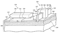
- One such alternative embodiment is illustrated in FIG. 3 .
- FIG. 3 is a perspective view for a portion of a semiconductor structure incorporating a first embodiment of the present invention.
- a planar transistor 330 such as a UTBSOIFET
- a multiple-gate transistor 320 such as a FinFET
- SOI substrate structure 340 comprises a substrate 342 , an insulator layer 344 , and a semiconductor layer 364 .
- the planar transistor 330 has a first active region 331 with a generally thin, planar shape.
- the multiple-gate transistor 320 has a second active region 322 with a generally tall, fin shape.
- the first and second active regions 331 , 322 are formed from a same semiconductor layer of the SOI structure 340 .
- the first active region 331 has a first thickness t 1 .
- the second active region 322 has a second thickness t 2 .
- the second thickness t 2 is larger than the first thickness t 1 .
- the first thickness t 1 is preferably less than about 400 angstroms, and even more preferably less than about 200 angstroms.
- the first thickness t 1 may be less than half of the gate length l g for the planar transistor 330 , and more preferably the first thickness t 1 is less than one third of the gate length l g .
- the first thickness t 1 may be less than 150 angstroms or more preferably less than 100 angstroms.
- the planar transistor 330 may be referred to as an ultra-thin body (UTB) transistor.
- a first gate dielectric 334 is overlying a first channel region in the first active region 331 .
- a first gate electrode 336 is overlying the first gate dielectric 334 .
- Source and drain regions 337 , 338 of the planar transistor 330 are formed in the first active region 331 oppositely adjacent the first gate electrode 336 .
- the second thickness t 2 (i.e., h f ) for the fin structure of the second active region 322 is preferably greater than about 100 angstroms, and more preferably greater than about 400 angstroms, for example.
- the fin width w f is preferably greater than about 500 angstroms.
- a second gate dielectric 324 is overlying a second channel region in the second active region 322 .
- the second gate dielectric 324 at least partially wraps around the second channel region of the fin.
- a second gate electrode 326 is overlying the second gate dielectric 324 .
- the second gate dielectric 324 electrically insulates the second gate electrode 326 from the fin of the second active region 322 .
- the second gate electrode 326 extends along three sides (along at least part of the two sidewalls and along the top surface of the fin) of the second channel region of the fin.
- Source and drain regions 327 , 328 of the multiple-gate transistor 320 are formed in the second active region 322 oppositely adjacent the second gate electrode 326 . Because a substantial fraction of the drive current flowing from the source 327 to the drain 328 flows on the sidewall surfaces, it is often advantageous to have a tall fin (see e.g., example dimensions described above) for the multiple-gate transistor 320 .
- the planar transistor 330 and/or the multiple-gate transistor 320 of FIG. 3 may also have spacers formed on the sidewalls of the gate electrodes 326 , 336 . Such spacers may be useful in doping the source and drain regions 327 , 328 , 337 , 338 , for example.
- the planar transistor 330 and/or the multiple-gate transistor 320 of an embodiment may have elevated source and drain regions, or raised source and drain regions (not shown).
- the source and drain regions may also be strapped with a conductive material such as a silicide. In such case, the spacers prevent conductive silicide material on the source and drain regions from making electrical contact with the gate electrode, which would lead to undesirable shorting of the source or drain regions to the gate electrode.
- FIG. 4 is a plan view of the devices illustrated in FIG. 3 , but with an n-FinFET 320 and a p-UTBSOIFET 330 laid out according to a preferred embodiment.
- both devices are on a ⁇ 110 ⁇ SOI, non-hybrid substrate.
- the Fin is aligned along a ⁇ 110> direction, i.e., the source 327 to drain 328 direction is ⁇ 110>, and the Fin's sidewall surface orientation is ⁇ 100 ⁇ .
- the Fin's two sidewalls form a ⁇ 100 ⁇ Schottky S/D silicide, which is in accordance with preferred embodiments (see NMOSFET 253 , FIG. 2 ).
- the p-UTBSOIFET 330 lies on a ⁇ 110 ⁇ substrate with a ⁇ 111> channel direction.
- the p-UTBSOIFET channel direction is ⁇ 110>, which is the direction of maximum hole mobility.
- FIG. 5 is a plan view of n-FinFET 320 and a p-FinFET 420 laid out according to a preferred embodiment.
- both devices are on a ⁇ 110 ⁇ SOI, non-hybrid substrate, and n-FinFET Fin is aligned along a ⁇ 110> direction, i.e., the source 327 to drain 328 direction is ⁇ 110>, and the Fin's sidewall surface orientation is ⁇ 100 ⁇ .
- the p-FinFET 420 in this embodiment is rotated about 55° with respect to the n-FinFET 320 .
- the p-FinFET 420 Fin is aligned along a ⁇ 211> direction, i.e., the source 427 to drain 428 direction is ⁇ 211>, and the Fin's sidewall surface orientation is ⁇ 111 ⁇ . Furthermore, the ends 430 of p-FinFET 420 Fins necessarily form a ⁇ 211 ⁇ Schottky S/D interface. Recalling the discussion above, the ⁇ 211 ⁇ interface has a lower Schottky barrier than the ⁇ 111 ⁇ interface. Therefore, this embodiment improves device performance due to the superior Schottky S/D configuration.
- the devices of FIG. 5 are formed on a hybrid SOI substrate with ⁇ 211 ⁇ and ⁇ 110 ⁇ orientations for p-FinFET 420 and n-FinFET 320 , respectively.
- the Schottky S/D barrier is reduced with the metal silicide sidewall facing ⁇ 100 ⁇ for n-FinFET 320 and ⁇ 110 ⁇ for p-FinFET 420 .
- the interfacial layer may comprise materials that have conductive, semi-conductive, and/or insulator-like properties.
- the interfacial layer comprises a silicide.
Landscapes
- Engineering & Computer Science (AREA)
- Power Engineering (AREA)
- Physics & Mathematics (AREA)
- Condensed Matter Physics & Semiconductors (AREA)
- General Physics & Mathematics (AREA)
- Computer Hardware Design (AREA)
- Microelectronics & Electronic Packaging (AREA)
- Manufacturing & Machinery (AREA)
- Metal-Oxide And Bipolar Metal-Oxide Semiconductor Integrated Circuits (AREA)
- Thin Film Transistor (AREA)
- Electrodes Of Semiconductors (AREA)
- Insulated Gate Type Field-Effect Transistor (AREA)
Priority Applications (4)
| Application Number | Priority Date | Filing Date | Title |
|---|---|---|---|
| US11/220,176 US7737532B2 (en) | 2005-09-06 | 2005-09-06 | Hybrid Schottky source-drain CMOS for high mobility and low barrier |
| TW095129773A TWI312544B (en) | 2005-09-06 | 2006-08-14 | Semiconductor device, cmos device and p-type semiconductor device |
| CN200610125733.3A CN1929139A (zh) | 2005-09-06 | 2006-08-29 | 半导体装置、cmos装置及p型半导体装置 |
| JP2006237361A JP4639172B2 (ja) | 2005-09-06 | 2006-09-01 | 半導体デバイス |
Applications Claiming Priority (1)
| Application Number | Priority Date | Filing Date | Title |
|---|---|---|---|
| US11/220,176 US7737532B2 (en) | 2005-09-06 | 2005-09-06 | Hybrid Schottky source-drain CMOS for high mobility and low barrier |
Publications (2)
| Publication Number | Publication Date |
|---|---|
| US20070052027A1 US20070052027A1 (en) | 2007-03-08 |
| US7737532B2 true US7737532B2 (en) | 2010-06-15 |
Family
ID=37829268
Family Applications (1)
| Application Number | Title | Priority Date | Filing Date |
|---|---|---|---|
| US11/220,176 Active 2027-06-22 US7737532B2 (en) | 2005-09-06 | 2005-09-06 | Hybrid Schottky source-drain CMOS for high mobility and low barrier |
Country Status (4)
| Country | Link |
|---|---|
| US (1) | US7737532B2 (zh) |
| JP (1) | JP4639172B2 (zh) |
| CN (1) | CN1929139A (zh) |
| TW (1) | TWI312544B (zh) |
Cited By (7)
| Publication number | Priority date | Publication date | Assignee | Title |
|---|---|---|---|---|
| US20090206416A1 (en) * | 2008-02-19 | 2009-08-20 | International Business Machines Corporation | Dual metal gate structures and methods |
| US20100270621A1 (en) * | 2009-04-23 | 2010-10-28 | Nec Electronics Corporation | Semiconductor device and method of manufacturing the semiconductor device |
| US8236634B1 (en) * | 2011-03-17 | 2012-08-07 | International Business Machines Corporation | Integration of fin-based devices and ETSOI devices |
| US20130320294A1 (en) * | 2011-12-23 | 2013-12-05 | Annalisa Cappellani | Common-substrate semiconductor devices having nanowires or semiconductor bodies with differing material orientation or composition |
| US8871600B2 (en) | 2011-11-11 | 2014-10-28 | International Business Machines Corporation | Schottky barrier diodes with a guard ring formed by selective epitaxy |
| US9466601B2 (en) | 2013-08-12 | 2016-10-11 | Samsung Electronics Co., Ltd. | Semiconductor device and method of fabricating the same |
| US20160336345A1 (en) * | 2014-04-29 | 2016-11-17 | International Business Machines Corporation | CHANNEL SiGe DEVICES WITH MULTIPLE THRESHOLD VOLTAGES ON HYBRID ORIENTED SUBSTRATES, AND METHODS OF MANUFACTURING SAME |
Families Citing this family (20)
| Publication number | Priority date | Publication date | Assignee | Title |
|---|---|---|---|---|
| US7575975B2 (en) * | 2005-10-31 | 2009-08-18 | Freescale Semiconductor, Inc. | Method for forming a planar and vertical semiconductor structure having a strained semiconductor layer |
| JP4960007B2 (ja) * | 2006-04-26 | 2012-06-27 | 株式会社東芝 | 半導体装置及び半導体装置の製造方法 |
| US7897994B2 (en) * | 2007-06-18 | 2011-03-01 | Texas Instruments Incorporated | Method of making (100) NMOS and (110) PMOS sidewall surface on the same fin orientation for multiple gate MOSFET with DSB substrate |
| US7863712B2 (en) * | 2007-10-30 | 2011-01-04 | International Business Machines Corporation | Hybrid orientation semiconductor structure with reduced boundary defects and method of forming same |
| EP2073267A1 (en) * | 2007-12-19 | 2009-06-24 | INTERUNIVERSITAIR MICROELEKTRONICA CENTRUM vzw (IMEC) | Method of fabricating multi-gate semiconductor devices and devices obtained |
| US7943479B2 (en) * | 2008-08-19 | 2011-05-17 | Texas Instruments Incorporated | Integration of high-k metal gate stack into direct silicon bonding (DSB) hybrid orientation technology (HOT) pMOS process flow |
| US8241970B2 (en) | 2008-08-25 | 2012-08-14 | International Business Machines Corporation | CMOS with channel P-FinFET and channel N-FinFET having different crystalline orientations and parallel fins |
| JP5700621B2 (ja) * | 2009-04-24 | 2015-04-15 | 株式会社半導体エネルギー研究所 | 半導体装置の作製方法 |
| US8232627B2 (en) * | 2009-09-21 | 2012-07-31 | International Business Machines Corporation | Integrated circuit device with series-connected field effect transistors and integrated voltage equalization and method of forming the device |
| CN101771088A (zh) * | 2010-01-21 | 2010-07-07 | 复旦大学 | Pn结和肖特基结混合式二极管及其制备方法 |
| US9209180B2 (en) * | 2010-02-10 | 2015-12-08 | Taiwan Semiconductor Manufacturing Company, Ltd. | Field effect transistor with conduction band electron channel and uni-terminal response |
| US9184050B2 (en) * | 2010-07-30 | 2015-11-10 | Taiwan Semiconductor Manufacturing Company, Ltd. | Inverted trapezoidal recess for epitaxial growth |
| US8378394B2 (en) | 2010-09-07 | 2013-02-19 | International Business Machines Corporation | Method for forming and structure of a recessed source/drain strap for a MUGFET |
| US9082751B2 (en) | 2011-09-14 | 2015-07-14 | Broadcom Corporation | Half-FinFET semiconductor device and related method |
| US9406518B2 (en) * | 2011-11-18 | 2016-08-02 | Taiwan Semiconductor Manufacturing Company, Ltd. | (110) surface orientation for reducing fermi-level-pinning between high-K dielectric and group III-V compound semiconductor substrate |
| US8941187B2 (en) * | 2012-01-13 | 2015-01-27 | Globalfoundries Inc. | Strain engineering in three-dimensional transistors based on strained isolation material |
| US9059044B2 (en) | 2012-11-15 | 2015-06-16 | International Business Machines Corporation | On-chip diode with fully depleted semiconductor devices |
| JP6533237B2 (ja) * | 2014-06-20 | 2019-06-19 | インテル・コーポレーション | 高電圧トランジスタ及び低電圧非プレーナ型トランジスタのモノリシック集積 |
| US11610887B2 (en) * | 2019-01-09 | 2023-03-21 | Intel Corporation | Side-by-side integration of III-n transistors and thin-film transistors |
| DE102020112203A1 (de) * | 2020-03-13 | 2021-09-16 | Taiwan Semiconductor Manufacturing Co. Ltd. | Verfahren zum einbetten planarer fets mit finfets |
Citations (11)
| Publication number | Priority date | Publication date | Assignee | Title |
|---|---|---|---|---|
| US4857986A (en) | 1985-10-17 | 1989-08-15 | Kabushiki Kaisha Toshiba | Short channel CMOS on 110 crystal plane |
| US5384473A (en) | 1991-10-01 | 1995-01-24 | Kabushiki Kaisha Toshiba | Semiconductor body having element formation surfaces with different orientations |
| US6096590A (en) * | 1996-07-18 | 2000-08-01 | International Business Machines Corporation | Scalable MOS field effect transistor |
| US6261932B1 (en) | 1999-07-29 | 2001-07-17 | Fairchild Semiconductor Corp. | Method of fabricating Schottky diode and related structure |
| US20040041226A1 (en) | 2002-05-16 | 2004-03-04 | Snyder John P. | Schottky barrier CMOS device and method |
| US6744103B2 (en) | 1999-12-16 | 2004-06-01 | Spinnaker Semiconductor, Inc. | Short-channel schottky-barrier MOSFET device and manufacturing method |
| US20040113171A1 (en) | 2002-12-13 | 2004-06-17 | Taiwan Semiconductor Manufacturing Company | Method of fabricating a mosfet device with metal containing gate structures |
| US6784035B2 (en) | 2002-01-23 | 2004-08-31 | Spinnaker Semiconductor, Inc. | Field effect transistor having source and/or drain forming Schottky or Schottky-like contact with strained semiconductor substrate |
| US20040266076A1 (en) | 2003-06-26 | 2004-12-30 | International Business Machines Corporation | HYBRID PLANAR AND FinFET CMOS DEVICES |
| US7235433B2 (en) * | 2004-11-01 | 2007-06-26 | Advanced Micro Devices, Inc. | Silicon-on-insulator semiconductor device with silicon layers having different crystal orientations and method of forming the silicon-on-insulator semiconductor device |
| US7298009B2 (en) * | 2005-02-01 | 2007-11-20 | Infineon Technologies Ag | Semiconductor method and device with mixed orientation substrate |
Family Cites Families (6)
| Publication number | Priority date | Publication date | Assignee | Title |
|---|---|---|---|---|
| JPH04372166A (ja) * | 1991-06-21 | 1992-12-25 | Matsushita Electric Ind Co Ltd | 半導体装置の製造方法 |
| US7329923B2 (en) * | 2003-06-17 | 2008-02-12 | International Business Machines Corporation | High-performance CMOS devices on hybrid crystal oriented substrates |
| JPWO2005022637A1 (ja) * | 2003-08-28 | 2007-11-01 | 日本電気株式会社 | フィン型電界効果トランジスタを有する半導体装置 |
| JP2005079277A (ja) * | 2003-08-29 | 2005-03-24 | Toshiba Corp | 電界効果トランジスタ |
| JP4439358B2 (ja) * | 2003-09-05 | 2010-03-24 | 株式会社東芝 | 電界効果トランジスタ及びその製造方法 |
| JP2006278818A (ja) * | 2005-03-30 | 2006-10-12 | Renesas Technology Corp | 半導体装置 |
-
2005
- 2005-09-06 US US11/220,176 patent/US7737532B2/en active Active
-
2006
- 2006-08-14 TW TW095129773A patent/TWI312544B/zh active
- 2006-08-29 CN CN200610125733.3A patent/CN1929139A/zh active Pending
- 2006-09-01 JP JP2006237361A patent/JP4639172B2/ja active Active
Patent Citations (13)
| Publication number | Priority date | Publication date | Assignee | Title |
|---|---|---|---|---|
| US4857986A (en) | 1985-10-17 | 1989-08-15 | Kabushiki Kaisha Toshiba | Short channel CMOS on 110 crystal plane |
| US5384473A (en) | 1991-10-01 | 1995-01-24 | Kabushiki Kaisha Toshiba | Semiconductor body having element formation surfaces with different orientations |
| US6096590A (en) * | 1996-07-18 | 2000-08-01 | International Business Machines Corporation | Scalable MOS field effect transistor |
| US6261932B1 (en) | 1999-07-29 | 2001-07-17 | Fairchild Semiconductor Corp. | Method of fabricating Schottky diode and related structure |
| US6744103B2 (en) | 1999-12-16 | 2004-06-01 | Spinnaker Semiconductor, Inc. | Short-channel schottky-barrier MOSFET device and manufacturing method |
| US20050003595A1 (en) | 2002-01-23 | 2005-01-06 | Snyder John P. | Field effect transistor having source and/or drain forming Schottky or Schottky-like contact with strained semiconductor substrate |
| US6784035B2 (en) | 2002-01-23 | 2004-08-31 | Spinnaker Semiconductor, Inc. | Field effect transistor having source and/or drain forming Schottky or Schottky-like contact with strained semiconductor substrate |
| US20040041226A1 (en) | 2002-05-16 | 2004-03-04 | Snyder John P. | Schottky barrier CMOS device and method |
| US20040113171A1 (en) | 2002-12-13 | 2004-06-17 | Taiwan Semiconductor Manufacturing Company | Method of fabricating a mosfet device with metal containing gate structures |
| US20040266076A1 (en) | 2003-06-26 | 2004-12-30 | International Business Machines Corporation | HYBRID PLANAR AND FinFET CMOS DEVICES |
| US6911383B2 (en) * | 2003-06-26 | 2005-06-28 | International Business Machines Corporation | Hybrid planar and finFET CMOS devices |
| US7235433B2 (en) * | 2004-11-01 | 2007-06-26 | Advanced Micro Devices, Inc. | Silicon-on-insulator semiconductor device with silicon layers having different crystal orientations and method of forming the silicon-on-insulator semiconductor device |
| US7298009B2 (en) * | 2005-02-01 | 2007-11-20 | Infineon Technologies Ag | Semiconductor method and device with mixed orientation substrate |
Non-Patent Citations (17)
| Title |
|---|
| Connelly, D. et al., "Performance Advantage of Schottky Source/Drain in Ultrathin-Body Silicon-on-Insulator and Dual-Gate CMOS," IEEE Transactions in Electron Devices, May 2003, pp. 1340-1345, vol. 50, No. 5. |
| Connelly, D., at al., "Optimizing Schottky S/D Offset for 25-nm Dual-Gate CMOS Performance," IEEE Electron Device Letters, Jun. 2003, pp. 411-413, vol. 24, No. 6. |
| Connelly, D., et al., "A New Route to Zero-Barrier Metal Source/Drain MOSFETs," IEEE Transactions on Nanotechnology, Mar. 2004, pp. 98-104, vol. 3, No. 1. |
| Doris, B., et al., "A Simplified Hybrid Orientation Technology (SHOT) for High Performance CMOS," Symposium on VLSI Technology Digest of Technical Papers, IEEE, 2004, pp. 86-87. |
| Hwang, J. R., et al., "Symmetrical 45nm PMOS on (110) Substrate with Excellent S/D Extension Distribution and Mobility Enhancement," Symposium on VLSI Technology Digest of Technical Papers, IEEE, 2004, pp. 90-91. |
| Kedzierski, J., et al., "Complementary silicide source/drain thin-body MOSFETs for the 20nm gate length regime," IEDM, 2000, pp. 57-60. |
| Kinoshita, a., et al., "Solution for High-Performance Schottky-Source/Drain MOSFETs: Schottky Barrier Height Engineering with Dopant Segregation Technique," Symposium on VLSI Technology Digest of Technical Papers, IEEE, 2004, pp. 168-169. |
| Lin, H.-C., et al., "High-Performance P-Channel Schottky-Barrier SOI FinFET Featuring Self-Aligned PtSi Source/Drain and Electrical Junctions," IEEE Electron Device Letters, Feb. 2003, pp. 102-104, vol. 24, No. 2. |
| Liu, C.W., et al., "Mobility-Enhancement Technologies," IEEE Circuits & Devices Magazine, May/Jun. 2005, pp. 21-36. |
| Michaelson, H.B., "The work function of the elements and its periodicity," Journal of Applied Physics, vol. 48, No. 11, Nov. 1977, pp. 4729-4733. |
| Sullivan, J. P. et al., "Correlation of the interfacial structure and electrical properties of epitaxial silicides on Si," J. Vac. Sci. Technol., American Vacuum Society, Jul./Aug. 1992, pp. 1959-1964, vol. A 10, No. 4. |
| Tung, R. T., et al., "Expitaxial metal-semiconductor structures and their properties," J. Vac. Sci. Technol., American Vacuum Society, Nov./Dec. 1986, pp. 1435-1443, vol. B 4, No. 6. |
| Tung, R. T., et al., "Schottky-barrier heights of single-crystal NiSi2 on Si(111): The effect of a surface p-n junction," Physical Review, The American Physical Society, May 15, 1986, pp. 7077-7090, vol. 33, No. 10. |
| Tung, R. T., et al., "Schottky-Barrier Inhomogeneity at Epitaxial NiSi2 Interfaces on Si(100)," Physical Review Letters, Jan. 7, 1991, pp. 72-75, vol. 66, No. 1. |
| Werner, P., et al., "Interface structure and Schottky barrier height of buried CoSi2/Si(001) layers," J. Appl. Phys., American Institute of Physics, Sep. 15, 1993, pp. 3846-3854, vol. 74, No. 6. |
| Yang, F.-L., et al., "5nm-Gate Nanowire FinFET," Symposium on VLSI Technology Digest of Technical Papers, IEEE, 2004, pp. 196-197. |
| Yang, M., et al., "On the Integration of CMOS and Hybrid Crystal Orientations," Symposium on VLSI Technology Digest of Technical Papers, IEEE, 2004, pp. 160-161. |
Cited By (15)
| Publication number | Priority date | Publication date | Assignee | Title |
|---|---|---|---|---|
| US20090206416A1 (en) * | 2008-02-19 | 2009-08-20 | International Business Machines Corporation | Dual metal gate structures and methods |
| US20100270621A1 (en) * | 2009-04-23 | 2010-10-28 | Nec Electronics Corporation | Semiconductor device and method of manufacturing the semiconductor device |
| US8269271B2 (en) * | 2009-04-23 | 2012-09-18 | Renesas Electronics Corporation | Hybrid planarFET and FinFET provided on a chip |
| US8586437B2 (en) | 2009-04-23 | 2013-11-19 | Renesas Electronics Corporation | Semiconductor device and method of manufacturing the semiconductor device |
| US8236634B1 (en) * | 2011-03-17 | 2012-08-07 | International Business Machines Corporation | Integration of fin-based devices and ETSOI devices |
| US20120261756A1 (en) * | 2011-03-17 | 2012-10-18 | International Business Machines Corporation | Integration of fin-based devices and etsoi devices |
| US8779511B2 (en) * | 2011-03-17 | 2014-07-15 | International Business Machines Corporation | Integration of fin-based devices and ETSOI devices |
| US8871600B2 (en) | 2011-11-11 | 2014-10-28 | International Business Machines Corporation | Schottky barrier diodes with a guard ring formed by selective epitaxy |
| US20130320294A1 (en) * | 2011-12-23 | 2013-12-05 | Annalisa Cappellani | Common-substrate semiconductor devices having nanowires or semiconductor bodies with differing material orientation or composition |
| US9559160B2 (en) * | 2011-12-23 | 2017-01-31 | Intel Corporation | Common-substrate semiconductor devices having nanowires or semiconductor bodies with differing material orientation or composition |
| US9466601B2 (en) | 2013-08-12 | 2016-10-11 | Samsung Electronics Co., Ltd. | Semiconductor device and method of fabricating the same |
| US9711506B2 (en) | 2013-08-12 | 2017-07-18 | Samsung Electronics Co., Ltd. | Semiconductor device and method of fabricating the same |
| US10177150B2 (en) | 2013-08-12 | 2019-01-08 | Samsung Electronics Co., Ltd. | Semiconductor device and method of fabricating the same |
| US20160336345A1 (en) * | 2014-04-29 | 2016-11-17 | International Business Machines Corporation | CHANNEL SiGe DEVICES WITH MULTIPLE THRESHOLD VOLTAGES ON HYBRID ORIENTED SUBSTRATES, AND METHODS OF MANUFACTURING SAME |
| US10312259B2 (en) * | 2014-04-29 | 2019-06-04 | International Business Machines Corporation | Channel SiGe devices with multiple threshold voltages on hybrid oriented substrates, and methods of manufacturing same |
Also Published As
| Publication number | Publication date |
|---|---|
| JP4639172B2 (ja) | 2011-02-23 |
| CN1929139A (zh) | 2007-03-14 |
| TW200713467A (en) | 2007-04-01 |
| US20070052027A1 (en) | 2007-03-08 |
| TWI312544B (en) | 2009-07-21 |
| JP2007073960A (ja) | 2007-03-22 |
Similar Documents
| Publication | Publication Date | Title |
|---|---|---|
| US7737532B2 (en) | Hybrid Schottky source-drain CMOS for high mobility and low barrier | |
| CN110718588B (zh) | 高性能mosfet | |
| US11756960B2 (en) | Multi-threshold voltage gate-all-around transistors | |
| US10020230B2 (en) | FinFETs with multiple threshold voltages | |
| US20190131189A1 (en) | Gate all-around semiconductor device and manufacturing method thereof | |
| US10833204B2 (en) | Multiple width nanosheet devices | |
| US11923413B2 (en) | Semiconductor structure with extended contact structure | |
| US7405449B2 (en) | Semiconductor device and method of manufacturing the same | |
| EP3711098A1 (en) | Replacement metal gate processes for vertical transport field-effect transistor | |
| US20080227241A1 (en) | Method of fabricating semiconductor device | |
| US20200227305A1 (en) | Dielectric isolation for nanosheet devices | |
| JP2009503902A (ja) | 半導体金属合金への完全変換により得られる金属ゲートmosfet及びその製造方法 | |
| US11695038B2 (en) | Forming single and double diffusion breaks for fin field-effect transistor structures | |
| JP2014038898A (ja) | 半導体装置 | |
| KR20190056341A (ko) | 듀얼 게이트 유전체 트랜지스터 | |
| CN108475693B (zh) | 具有可调功函数的场效应晶体管叠层 | |
| US20220406909A1 (en) | Field effect transistor with dual silicide and method | |
| US10892339B2 (en) | Gate first technique in vertical transport FET using doped silicon gates with silicide | |
| US20240038867A1 (en) | Isolation pillar structures for stacked device structures | |
| US20240063217A1 (en) | Semiconductor structures with back side transistor devices | |
| US20240079462A1 (en) | Vertical transport transistor devices with back side interconnects | |
| US20230402520A1 (en) | Staircase stacked field effect transistor | |
| TW202333381A (zh) | 半導體元件及其製造方法 | |
| TW202349722A (zh) | 半導體結構及其製造方法 | |
| CN111653623A (zh) | 鳍式晶体管结构 |
Legal Events
| Date | Code | Title | Description |
|---|---|---|---|
| AS | Assignment |
Owner name: TAIWAN SEMICONDUCTOR MANUFACTURING COMPANY, LTD.,T Free format text: ASSIGNMENT OF ASSIGNORS INTEREST;ASSIGNORS:KE, CHUNG-HU;KO, CHIH-HSIN;CHEN, HUNG-WEI;AND OTHERS;SIGNING DATES FROM 20050629 TO 20050827;REEL/FRAME:016965/0485 Owner name: TAIWAN SEMICONDUCTOR MANUFACTURING COMPANY, LTD., Free format text: ASSIGNMENT OF ASSIGNORS INTEREST;ASSIGNORS:KE, CHUNG-HU;KO, CHIH-HSIN;CHEN, HUNG-WEI;AND OTHERS;REEL/FRAME:016965/0485;SIGNING DATES FROM 20050629 TO 20050827 |
|
| STCF | Information on status: patent grant |
Free format text: PATENTED CASE |
|
| CC | Certificate of correction | ||
| FPAY | Fee payment |
Year of fee payment: 4 |
|
| MAFP | Maintenance fee payment |
Free format text: PAYMENT OF MAINTENANCE FEE, 8TH YEAR, LARGE ENTITY (ORIGINAL EVENT CODE: M1552) Year of fee payment: 8 |
|
| MAFP | Maintenance fee payment |
Free format text: PAYMENT OF MAINTENANCE FEE, 12TH YEAR, LARGE ENTITY (ORIGINAL EVENT CODE: M1553); ENTITY STATUS OF PATENT OWNER: LARGE ENTITY Year of fee payment: 12 |