US7732333B2 - Process for producing and apparatus for improving the bonding between a plastic and a metal - Google Patents
Process for producing and apparatus for improving the bonding between a plastic and a metal Download PDFInfo
- Publication number
- US7732333B2 US7732333B2 US10/575,798 US57579804A US7732333B2 US 7732333 B2 US7732333 B2 US 7732333B2 US 57579804 A US57579804 A US 57579804A US 7732333 B2 US7732333 B2 US 7732333B2
- Authority
- US
- United States
- Prior art keywords
- interlayer
- silver
- leadframe
- etching
- approx
- Prior art date
- Legal status (The legal status is an assumption and is not a legal conclusion. Google has not performed a legal analysis and makes no representation as to the accuracy of the status listed.)
- Active, expires
Links
- 239000004033 plastic Substances 0.000 title claims abstract description 20
- 229920003023 plastic Polymers 0.000 title claims abstract description 20
- 238000000034 method Methods 0.000 title claims description 52
- 239000002184 metal Substances 0.000 title 1
- 239000011229 interlayer Substances 0.000 claims abstract description 105
- 239000004065 semiconductor Substances 0.000 claims abstract description 38
- 150000001875 compounds Chemical class 0.000 claims abstract description 10
- 239000000463 material Substances 0.000 claims abstract description 9
- 239000011159 matrix material Substances 0.000 claims abstract description 6
- 238000005530 etching Methods 0.000 claims description 36
- BQCADISMDOOEFD-UHFFFAOYSA-N Silver Chemical compound [Ag] BQCADISMDOOEFD-UHFFFAOYSA-N 0.000 claims description 30
- 229910052709 silver Inorganic materials 0.000 claims description 30
- 239000004332 silver Substances 0.000 claims description 30
- 239000010410 layer Substances 0.000 claims description 29
- PXHVJJICTQNCMI-UHFFFAOYSA-N Nickel Chemical compound [Ni] PXHVJJICTQNCMI-UHFFFAOYSA-N 0.000 claims description 26
- 229910001316 Ag alloy Inorganic materials 0.000 claims description 16
- 229910052759 nickel Inorganic materials 0.000 claims description 13
- 239000000126 substance Substances 0.000 claims description 11
- 239000000203 mixture Substances 0.000 claims description 10
- 229940100890 silver compound Drugs 0.000 claims description 10
- 150000003379 silver compounds Chemical class 0.000 claims description 10
- 238000005275 alloying Methods 0.000 claims description 9
- 238000005234 chemical deposition Methods 0.000 claims description 4
- 238000000151 deposition Methods 0.000 claims description 4
- 238000004070 electrodeposition Methods 0.000 claims description 4
- 238000005538 encapsulation Methods 0.000 claims description 2
- 239000000470 constituent Substances 0.000 claims 2
- QAOWNCQODCNURD-UHFFFAOYSA-N Sulfuric acid Chemical compound OS(O)(=O)=O QAOWNCQODCNURD-UHFFFAOYSA-N 0.000 description 12
- 238000004519 manufacturing process Methods 0.000 description 11
- 230000008901 benefit Effects 0.000 description 7
- VYPSYNLAJGMNEJ-UHFFFAOYSA-N Silicium dioxide Chemical compound O=[Si]=O VYPSYNLAJGMNEJ-UHFFFAOYSA-N 0.000 description 3
- 238000004873 anchoring Methods 0.000 description 3
- 238000005422 blasting Methods 0.000 description 3
- 238000004140 cleaning Methods 0.000 description 3
- 238000010790 dilution Methods 0.000 description 3
- 239000012895 dilution Substances 0.000 description 3
- 238000001000 micrograph Methods 0.000 description 3
- XLYOFNOQVPJJNP-UHFFFAOYSA-N water Substances O XLYOFNOQVPJJNP-UHFFFAOYSA-N 0.000 description 3
- 229910001030 Iron–nickel alloy Inorganic materials 0.000 description 2
- 239000000956 alloy Substances 0.000 description 2
- 230000015572 biosynthetic process Effects 0.000 description 2
- 239000007767 bonding agent Substances 0.000 description 2
- 230000008021 deposition Effects 0.000 description 2
- 239000002245 particle Substances 0.000 description 2
- 238000005240 physical vapour deposition Methods 0.000 description 2
- 230000007704 transition Effects 0.000 description 2
- RYGMFSIKBFXOCR-UHFFFAOYSA-N Copper Chemical compound [Cu] RYGMFSIKBFXOCR-UHFFFAOYSA-N 0.000 description 1
- QPLDLSVMHZLSFG-UHFFFAOYSA-N Copper oxide Chemical class [Cu]=O QPLDLSVMHZLSFG-UHFFFAOYSA-N 0.000 description 1
- HCHKCACWOHOZIP-UHFFFAOYSA-N Zinc Chemical compound [Zn] HCHKCACWOHOZIP-UHFFFAOYSA-N 0.000 description 1
- 229910001297 Zn alloy Inorganic materials 0.000 description 1
- 230000006978 adaptation Effects 0.000 description 1
- 230000002730 additional effect Effects 0.000 description 1
- 229910045601 alloy Inorganic materials 0.000 description 1
- VXAUWWUXCIMFIM-UHFFFAOYSA-M aluminum;oxygen(2-);hydroxide Chemical compound [OH-].[O-2].[Al+3] VXAUWWUXCIMFIM-UHFFFAOYSA-M 0.000 description 1
- 239000003795 chemical substances by application Substances 0.000 description 1
- 238000005229 chemical vapour deposition Methods 0.000 description 1
- 229910052802 copper Inorganic materials 0.000 description 1
- 239000010949 copper Substances 0.000 description 1
- 238000005238 degreasing Methods 0.000 description 1
- 210000001787 dendrite Anatomy 0.000 description 1
- 238000001035 drying Methods 0.000 description 1
- 230000005496 eutectics Effects 0.000 description 1
- 238000011156 evaluation Methods 0.000 description 1
- 239000012535 impurity Substances 0.000 description 1
- 238000005259 measurement Methods 0.000 description 1
- 230000035515 penetration Effects 0.000 description 1
- 238000005554 pickling Methods 0.000 description 1
- 238000004886 process control Methods 0.000 description 1
- 238000007788 roughening Methods 0.000 description 1
- 239000004576 sand Substances 0.000 description 1
- 238000007789 sealing Methods 0.000 description 1
- 235000012239 silicon dioxide Nutrition 0.000 description 1
- 239000000377 silicon dioxide Substances 0.000 description 1
- BSWGGJHLVUUXTL-UHFFFAOYSA-N silver zinc Chemical compound [Zn].[Ag] BSWGGJHLVUUXTL-UHFFFAOYSA-N 0.000 description 1
- 239000002356 single layer Substances 0.000 description 1
- 230000003746 surface roughness Effects 0.000 description 1
- 239000011800 void material Substances 0.000 description 1
- 238000007704 wet chemistry method Methods 0.000 description 1
- 239000011701 zinc Substances 0.000 description 1
- 229910052725 zinc Inorganic materials 0.000 description 1
Images


Classifications
-
- H—ELECTRICITY
- H01—ELECTRIC ELEMENTS
- H01L—SEMICONDUCTOR DEVICES NOT COVERED BY CLASS H10
- H01L23/00—Details of semiconductor or other solid state devices
- H01L23/48—Arrangements for conducting electric current to or from the solid state body in operation, e.g. leads, terminal arrangements ; Selection of materials therefor
- H01L23/488—Arrangements for conducting electric current to or from the solid state body in operation, e.g. leads, terminal arrangements ; Selection of materials therefor consisting of soldered or bonded constructions
- H01L23/495—Lead-frames or other flat leads
- H01L23/49579—Lead-frames or other flat leads characterised by the materials of the lead frames or layers thereon
- H01L23/49582—Metallic layers on lead frames
-
- H—ELECTRICITY
- H01—ELECTRIC ELEMENTS
- H01L—SEMICONDUCTOR DEVICES NOT COVERED BY CLASS H10
- H01L21/00—Processes or apparatus adapted for the manufacture or treatment of semiconductor or solid state devices or of parts thereof
- H01L21/02—Manufacture or treatment of semiconductor devices or of parts thereof
- H01L21/04—Manufacture or treatment of semiconductor devices or of parts thereof the devices having potential barriers, e.g. a PN junction, depletion layer or carrier concentration layer
- H01L21/48—Manufacture or treatment of parts, e.g. containers, prior to assembly of the devices, using processes not provided for in a single one of the subgroups H01L21/06 - H01L21/326
- H01L21/4814—Conductive parts
- H01L21/4821—Flat leads, e.g. lead frames with or without insulating supports
- H01L21/4828—Etching
-
- H—ELECTRICITY
- H01—ELECTRIC ELEMENTS
- H01L—SEMICONDUCTOR DEVICES NOT COVERED BY CLASS H10
- H01L23/00—Details of semiconductor or other solid state devices
- H01L23/48—Arrangements for conducting electric current to or from the solid state body in operation, e.g. leads, terminal arrangements ; Selection of materials therefor
- H01L23/488—Arrangements for conducting electric current to or from the solid state body in operation, e.g. leads, terminal arrangements ; Selection of materials therefor consisting of soldered or bonded constructions
- H01L23/495—Lead-frames or other flat leads
- H01L23/49503—Lead-frames or other flat leads characterised by the die pad
-
- H—ELECTRICITY
- H01—ELECTRIC ELEMENTS
- H01L—SEMICONDUCTOR DEVICES NOT COVERED BY CLASS H10
- H01L2924/00—Indexing scheme for arrangements or methods for connecting or disconnecting semiconductor or solid-state bodies as covered by H01L24/00
- H01L2924/0001—Technical content checked by a classifier
- H01L2924/0002—Not covered by any one of groups H01L24/00, H01L24/00 and H01L2224/00
Definitions
- the invention relates to a semiconductor having a leadframe or its base body for a semiconductor device, and a method of producing the semiconductor.
- a leadframe of this type is known from U.S. Pat. No. 5,554,569. This document describes a process for mechanically roughening the surface of a leadframe by bombardment with abrasive, microscopically small particles which include, inter alia, sand, silicon dioxide or aluminum dioxide.
- the leadframe described in U.S. Pat. No. 5,554,569 can scarcely be produced economically, since a dry process has to be carried out in addition to the wet-chemical processes used to clean and improve the leadframe surface in a closed production line with baths arranged spatially in succession. Moreover, a cleaning step has to be provided for in order to remove the residues of blasting agents from the leadframe surface.
- the present invention provides a semiconductor device which can always be operated reliably.
- the invention provides a leadframe or its base body having a roughened, three-dimensional surface, which offers greatly improved bonding for the encapsulating plastic in the semiconductor device.
- the production process according to the invention can easily and economically be integrated in the existing manufacturing sequence used to clean and improve the leadframe.
- the leadframe after stamping, is subjected to various wet-chemical and/or electrodeposition processes, such as degreasing, pickling and/or the application of various layers.
- a further interlayer is applied by a wet-chemical route, this further interlayer including nickel and/or silver and/or a silver-containing alloy or compound.
- this further interlayer including nickel and/or silver and/or a silver-containing alloy or compound.
- the surface of the applied interlayer is etched into in such a way that the interlayer acquires a three-dimensional surface structure.
- the leadframe is cleaned in order to remove all impurities which have collected on the surface.
- the advantage of this process for producing the leadframe according to the invention with improved bonding is that on account of the type of processes involved it is possible without major outlay to introduce the required manufacturing steps into an existing production line used to clean and improve leadframes.
- the application and etching of the interlayer according to the invention are carried out in separate baths, while existing tanks can be used for the final cleaning step.
- a further advantage for leadframes which are produced and processed in the form of endless strips compared to the prior art is that it is easy for additional baths to be integrated in the production line, which is being adapted to the endless form.
- the introduction of a chamber for the blasting process into an endless line entails major technical problems in particular on account of the sealing which is required at the entry to the chamber and the exit from the chamber.
- the advantage over a leadframe whose surface has been treated by means of blasting, in addition to the lower costs on account of simplified production, is also that the leadframe according to the invention, in accordance with the quality of the final cleaning step, is free of disruptive particles, which can cause the failure of a device.
- a particularly economical way of applying the silver required for the interlayer is deposition from an aqueous bath by means of conventional chemical deposition or electrodeposition processes, since such processes are easy to integrate in the existing manufacturing line used to clean and improve the leadframe.
- interlayers which include a silver alloy and/or silver compound and/or nickel.
- wet-chemical deposition processes are advantageous.
- the interlayer may in this case be applied as a single layer which serves only to produce a three-dimensional surface structure.
- a layer which comprises a plurality of individual layers is also possible and conceivable for a layer which comprises a plurality of individual layers to be applied instead of one homogeneous interlayer. This is desirable in particular if the interlayer, in addition to providing the three-dimensional surface structure, is also to perform further tasks.
- One conceivable use example in this respect is the application of an additional individual layer to a leadframe which includes copper or an iron-nickel alloy, or Alloy 42, for eutectic devices, in which this additional individual layer acts as a mechanical buffer for compensating for stresses which occur during attachment of the semiconductor chip.
- the application of the interlayer is followed, as a further process, by a treatment of the surface in order to obtain the three-dimensional structure required to improve the bonding. It would be possible for this three-dimensional structure to be formed by the targeted formation of dendrites at the surface. However, for economic reasons and for simplicity of process control it is also advantageous to form a three-dimensional structure by etching into the surface of the interlayer, i.e., by the controlled production of voids in the surface.
- this three-dimensional structure is produced by coarse deposition or by relatively coarse regions or structures of nickel and/or silver and/or a silver alloy with a subsequent etch.
- the interlayer is a pure silver layer.
- the interlayer is a silver compound and/or nickel and/or a silver alloy, such as for example a silver-zinc alloy containing approx. 2% to approx. 5% zinc, it is advantageous for the compound component or the alloying component to be etched out in order to form the voids.
- a simple way of implementing the process according to the invention for producing a leadframe with an interlayer in accordance with the invention provides for a uniform treatment of the entire surface of the leadframe in accordance with the present invention.
- the leadframe may also be advantageous for only certain regions of the leadframe to be treated in accordance with the present invention, i.e., for the three-dimensional surface structure to be applied only to certain locations.
- One conceivable application is devices for the field of automotive engineering, in which a critical point is the penetration of moisture via extremely small gaps between leadframe and plastic. The size of these gaps can be reduced by the application of a frame with a surface structure which improves bonding according to the present invention around the semiconductor chip.
- the nature of the leadframe and/or of the finished device also determines the chemical composition of the interlayer. Depending on, for example, the required electrical and thermal conductivity, the hardness and/or other desired mechanical properties, either a pure silver layer and/or a silver alloy and/or a silver compound and/or nickel may be advantageous.
- the surface of the interlayer according to the invention has a geometry as described below.
- the typical roughness average R a or waviness and/or surface roughness average S a is between approx. 0.1 ⁇ m and approx. 0.9 ⁇ m, preferably between approx. 0.1 ⁇ m and approx. 0.5 ⁇ m.
- the matrix of islands of remaining material typically has a mean width of approx. 0.5 ⁇ m, and the voids located therein typically have a width of approx. 2 ⁇ m.
- the geometry of the surface of the interlayer according to the invention can also be described by the ratio of islands to voids. Evaluation of a typical surface according to the present invention provides the following results: the ratio of the surface areas of islands to voids is typically in the range between approx. 2:1 and approx. 1:2.
- interlayers with different compositions than those which have been mentioned thus far.
- materials which produce interlayers which can be used for conventional chip attachment processes and conventional contact-connection processes are particularly advantageous.
- interlayer according to the invention it is conceivable and possible for the interlayer according to the invention to be applied not by means of wet-chemical methods, but rather by chemical or physical vapor deposition processes, i.e., CVD or PVD.
- An embodiment of this type is advantageous if extremely high demands are imposed on the purity of the resulting interlayer.
- FIG. 1 illustrates a cross section through a semiconductor device according to the invention
- FIG. 2 illustrates the schematic structure of an interlayer in accordance with a first embodiment of the invention
- FIG. 3 illustrates the schematic structure of the interlayer according to the invention from FIG. 2 after an etching process has been carried out;
- FIG. 4 illustrates the schematic structure of a further interlayer according to the invention
- FIG. 5 illustrates the schematic structure of the interlayer according to the invention from FIG. 4 after an etching process has been carried out
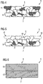
- FIG. 6 illustrates the schematic structure of an interlayer in accordance with a further embodiment of the invention.
- FIG. 7 illustrates the schematic structure of the interlayer according to the invention from FIG. 6 after an etching process has been carried out
- FIG. 8 illustrates the schematic structure of the transition between interlayer according to the invention and plastic in accordance with the first exemplary embodiment
- FIG. 9 illustrates the schematic structure of the transition between interlayer according to the invention and plastic in accordance with the exemplary embodiments from FIGS. 5 and 7 ;
- FIG. 10 illustrates a scanning electron microscope image of the surface of the interlayer according to the invention after the etching process has been carried out.
- FIG. 1 illustrates a greatly enlarged cross section through one embodiment of a semiconductor device 1 .
- the drawing is not to scale; the size ratios are illustrated on a distorted scale for the purpose of illustrating the schematic structure.
- the semiconductor device 1 has a base body 3 with interlayer 5 according to the invention.
- Semiconductor chip 2 and base body 3 are surrounded by a plastic compound 4 .
- FIG. 2 illustrates a greatly enlarged view, not to scale, of the schematic structure of the interlayer 5 according to the invention before the etching process is carried out.
- this interlayer 5 includes silver.
- the individual silver grains 8 which form a continuous surface 6 without voids 10 are illustrated in the figure.
- the underside 7 of the interlayer 5 is connected to the outer side of the leadframe (not shown here).
- FIG. 3 illustrates a greatly enlarged view, not to scale, of the schematic structure of the interlayer 5 according to the invention after the etching process has been carried out.
- this interlayer 5 includes silver.
- the underside 7 of the interlayer 5 is identical to that shown in FIG. 1 .
- the surface 6 now has voids 10 which have formed between the relatively small grains 9 of the surface 6 which has been etched into.
- FIG. 4 illustrates a greatly enlarged view, not to scale, of the schematic structure of the interlayer 5 according to an alternative embodiment of the invention before the etching process is carried out.
- this interlayer 5 includes a silver alloy. Therefore, in addition to the silver grains 8 , FIG. 4 also shows grains 11 which include the further alloying components.
- the interlayer 5 likewise has a surface 6 without voids 10 , but in this embodiment the surface is composed of silver grains 8 and grains of the alloying component 11 .
- the interlayer 5 of this embodiment is connected to the outer side of the leadframe (not shown here) via the underside 7 once again.
- FIG. 5 illustrates a greatly enlarged view, not to scale, of the schematic structure of the interlayer 5 in accordance with an alternative embodiment of the invention after the etching process has been carried out.
- the interlayer 5 includes a silver alloy, i.e., grains of the alloying component 11 are present in addition to the silver grains 8 .
- the underside 7 of the interlayer 5 is once again identical to that shown in FIG. 3 .
- the surface 6 has voids 10 which, unlike in FIG. 2 , have been formed by removing the grains of the alloying component 11 between the remaining silver grains 8 .
- the remaining silver grains 8 are of unchanged size.
- FIG. 6 illustrates a greatly enlarged view, not to scale, of the schematic structure of the interlayer 5 according to a further embodiment of the invention, once again before the etching process is carried out.
- the interlayer 5 includes two individual layers of different compositions; in the exemplary embodiment shown here, the lower individual layer 12 includes silver, while the upper individual layer 13 is formed from a silver alloy.
- the interlayer 5 is connected to the outer side of the leadframe (not shown here) via the underside 7 of the lower individual layer 12 .
- the structure of the upper individual layer 13 of this interlayer 5 corresponds to the structure shown in FIG. 3 , except that the underside of the upper individual layer 13 is not in direct contact with the leadframe, but rather represents the interface with the lower individual layer 12 .
- FIG. 7 illustrates a greatly enlarged view, not to scale, of the schematic structure of the interlayer 5 in accordance with a further embodiment of the invention after the etching process has been carried out.
- the surface structure formed in this embodiment is of similar type to that shown in FIG. 5 , i.e., it includes voids 10 which are formed by the removal of grains of the alloying component 11 , while leaving behind the silver grains 8 of unchanged size.
- FIG. 8 and FIG. 9 illustrate a greatly enlarged view, not to scale, of the schematic structure of the interlayer 5 according to the invention after the etching process has been carried out and after the application of the plastic 4 corresponding to the semiconductor device 1 .
- the plastic 4 has penetrated into the voids illustrated in FIGS. 3 , 5 and 7 .
- FIG. 10 illustrates a scanning electron microscope image of the three-dimensional structure of the surface 6 of the interlayer 5 in accordance with the first embodiment.
- the islands 14 of the remaining material with a typical mean diameter of approx. 0.5 ⁇ m can be recognized as light regions, surrounded by dark voids 10 with a typical mean void width of approx. 2 ⁇ m.
- a feature common to all the embodiments is that the etching process according to the invention modifies the surface 6 of an interlayer 5 which has been applied to the base body 3 for this purpose in such a way that voids 10 are formed in the surface 6 of the interlayer 5 , as diagrammatically depicted in FIGS. 3 , 5 and 7 .
- These voids 10 on account of their size and geometry, allow the plastic 4 of the semiconductor device 1 to be mechanically anchored on or interlocked with the surface 6 of the interlayer 5 , as diagrammatically depicted in FIGS. 8 and 9 .
- FIG. 6 and FIG. 7 illustrate a two-layer structure of the interlayer 5 .
- the upper individual layer 13 of the interlayer 5 is etched into in accordance with the invention in order to produce the three-dimensional structure for anchoring or interlocking the plastic 4 on the interlayer 5 .
- the lower individual layer 12 is applied in order to impart additional properties, such as for example a defined elasticity, to the interlayer 5 .
- the upper individual layer 13 and lower individual layer 12 may, but need not, have different chemical compositions. It is conceivable and possible for both individual layers to have the same chemical composition but to be deposited in different process steps and therefore to have different mechanical properties.
- FIG. 7 illustrates an embodiment having an upper individual layer 13 which includes a silver alloy.
- the lower individual layer 12 is not specified in more detail, and therefore may, for example, include nickel and/or silver and/or a silver alloy.
- the scanning electron microscope image in FIG. 10 illustrates the three-dimensional structure of the surface 6 of the interlayer 5 , which by virtue of the voids 10 creates spaces for the anchoring or interlocking of the plastic 4 on this surface 6 .
- the grain boundaries of the interlayer 5 which includes silver and had been applied to a nickel-plated leadframe, were etched into by means of sulfuric acid (H 2 SO 4 ) in accordance with the parameters listed in Table 1.
- sulfuric acid comprising approx. 96% strength sulfuric acid (H 2 SO 4 ) was produced by dilution with water in accordance with the values indicated in Table 1.
- the roughness average R a is defined as the arithmetic mean of the absolute profile deviation within the total measurement distance, equating to the height of a rectangle having the same surfaces as the surfaces between the profile centerline and the actual profile.
- a further result of these tests in accordance with the present invention was the range of possible roughness averages, i.e. the roughness averages for which the desired interlocking or anchoring of the plastic 4 at the surface 6 of the interlayer 5 is possible.
- the roughness averages R a are typically between 0.1 and 0.9 ⁇ m.
- the present invention as per the example shown here, it is possible to find a range of parameters for etching out the alloying components in the interlayer 5 which includes nickel and/or a silver alloy and/or a silver compound.
Landscapes
- Engineering & Computer Science (AREA)
- Physics & Mathematics (AREA)
- Condensed Matter Physics & Semiconductors (AREA)
- General Physics & Mathematics (AREA)
- Computer Hardware Design (AREA)
- Microelectronics & Electronic Packaging (AREA)
- Power Engineering (AREA)
- Manufacturing & Machinery (AREA)
- ing And Chemical Polishing (AREA)
- Lead Frames For Integrated Circuits (AREA)
- Die Bonding (AREA)
Applications Claiming Priority (4)
| Application Number | Priority Date | Filing Date | Title |
|---|---|---|---|
| DE10348715.8 | 2003-10-16 | ||
| DE10348715A DE10348715B4 (de) | 2003-10-16 | 2003-10-16 | Verfahren zum Herstellen eines Flachleiterrahmens mit verbesserter Haftung zwischen diesem und Kunststoff sowie Flachleiterrahmen |
| DE10348715 | 2003-10-16 | ||
| PCT/DE2004/002199 WO2005041272A2 (de) | 2003-10-16 | 2004-10-01 | Verfahren zur herstellung und vorrichtung zur verbesserung der haftung zwischen einem kunststoff und einem metall |
Related Parent Applications (1)
| Application Number | Title | Priority Date | Filing Date |
|---|---|---|---|
| PCT/EP2004/010610 A-371-Of-International WO2006032289A1 (de) | 2004-09-22 | 2004-09-22 | Medizinisches implantat |
Related Child Applications (1)
| Application Number | Title | Priority Date | Filing Date |
|---|---|---|---|
| US12/981,286 Continuation US8372110B2 (en) | 2004-09-22 | 2010-12-29 | Medical implant |
Publications (2)
| Publication Number | Publication Date |
|---|---|
| US20080258281A1 US20080258281A1 (en) | 2008-10-23 |
| US7732333B2 true US7732333B2 (en) | 2010-06-08 |
Family
ID=34484831
Family Applications (1)
| Application Number | Title | Priority Date | Filing Date |
|---|---|---|---|
| US10/575,798 Active 2025-06-29 US7732333B2 (en) | 2003-10-16 | 2004-10-01 | Process for producing and apparatus for improving the bonding between a plastic and a metal |
Country Status (4)
| Country | Link |
|---|---|
| US (1) | US7732333B2 (de) |
| EP (1) | EP1673800B1 (de) |
| DE (2) | DE10348715B4 (de) |
| WO (1) | WO2005041272A2 (de) |
Citations (24)
| Publication number | Priority date | Publication date | Assignee | Title |
|---|---|---|---|---|
| JPS5650551A (en) | 1979-10-02 | 1981-05-07 | Nec Corp | Lead frame for integrated circuit device |
| JPS5799763A (en) | 1980-12-12 | 1982-06-21 | Hitachi Cable Ltd | Manufacture of lead frame for integrated circuit |
| JPS61201797A (ja) | 1985-03-04 | 1986-09-06 | Matsushita Refrig Co | 熱交換器 |
| JPS6289891A (ja) | 1985-10-16 | 1987-04-24 | Matsushita Refrig Co | 熱交換器の製造方法 |
| JPS6293039A (ja) | 1985-10-18 | 1987-04-28 | Matsushita Refrig Co | 伝熱管のメツキ方法 |
| EP0335608A2 (de) | 1988-03-28 | 1989-10-04 | Texas Instruments Incorporated | Leiterrahmen mit verminderter Korrosion |
| US4883774A (en) | 1988-03-21 | 1989-11-28 | Motorola, Inc. | Silver flashing process on semiconductor leadframes |
| JPH0436478A (ja) | 1990-05-31 | 1992-02-06 | Toshiba Tungaloy Co Ltd | 多色被覆表面物品及びその製造方法 |
| EP0492952A1 (de) | 1990-12-18 | 1992-07-01 | Amkor Electronics, Inc. | Verfahren und Vorrichtung zur Herstellung eines Leiterrahmenbandes für IC-Chips in einem kontinuierlichen System |
| JPH04284650A (ja) | 1990-11-08 | 1992-10-09 | Natl Semiconductor Corp <Ns> | Oリングパッケージ |
| EP0579464A2 (de) | 1992-07-11 | 1994-01-19 | Shinko Electric Industries Co. Ltd. | Metallisches Insert und Verfahren zu seiner Oberflächenaufrauhung |
| US5554569A (en) * | 1994-06-06 | 1996-09-10 | Motorola, Inc. | Method and apparatus for improving interfacial adhesion between a polymer and a metal |
| JPH08264957A (ja) | 1995-03-23 | 1996-10-11 | Nec Corp | 多層印刷配線板の製造方法 |
| US5597760A (en) * | 1995-01-25 | 1997-01-28 | Nec Corporation | Process of fabricating semiconductor device having capacitor increased in capacitance by roughening surface of accumulating electrode |
| US5753535A (en) | 1991-09-18 | 1998-05-19 | Fujitsu Limited | Leadframe and resin-sealed semiconductor device |
| WO2000042405A1 (en) | 1999-01-15 | 2000-07-20 | Maxim Integrated Products, Inc. | Rigid encapsulation package for semiconductor pressure sensors |
| US6117566A (en) | 1997-02-03 | 2000-09-12 | Nippon Denkai, Ltd. | Lead frame material |
| US6194777B1 (en) | 1998-06-27 | 2001-02-27 | Texas Instruments Incorporated | Leadframes with selective palladium plating |
| US20010008305A1 (en) | 1998-06-10 | 2001-07-19 | Asat Ltd. | Leadless plastic chip carrier with etch back pad singulation |
| US6294100B1 (en) | 1998-06-10 | 2001-09-25 | Asat Ltd | Exposed die leadless plastic chip carrier |
| US20020048825A1 (en) | 2000-08-29 | 2002-04-25 | Phillip Young | Process to remove semiconductor chips from a plastic package |
| US6498099B1 (en) | 1998-06-10 | 2002-12-24 | Asat Ltd. | Leadless plastic chip carrier with etch back pad singulation |
| US20030197199A1 (en) | 2000-01-31 | 2003-10-23 | Noriaki Sakamoto | Semiconductor device and semiconductor module |
| US20040183166A1 (en) * | 2003-03-17 | 2004-09-23 | Abbott Donald C. | Preplated leadframe without precious metal |
Family Cites Families (2)
| Publication number | Priority date | Publication date | Assignee | Title |
|---|---|---|---|---|
| JP2805380B2 (ja) * | 1990-06-01 | 1998-09-30 | 住友特殊金属株式会社 | リードフレーム材の微細エッチング方法 |
| JP3706533B2 (ja) * | 2000-09-20 | 2005-10-12 | 三洋電機株式会社 | 半導体装置および半導体モジュール |
-
2003
- 2003-10-16 DE DE10348715A patent/DE10348715B4/de not_active Expired - Fee Related
-
2004
- 2004-10-01 EP EP04789914A patent/EP1673800B1/de not_active Not-in-force
- 2004-10-01 US US10/575,798 patent/US7732333B2/en active Active
- 2004-10-01 DE DE502004003309T patent/DE502004003309D1/de active Active
- 2004-10-01 WO PCT/DE2004/002199 patent/WO2005041272A2/de active Application Filing
Patent Citations (24)
| Publication number | Priority date | Publication date | Assignee | Title |
|---|---|---|---|---|
| JPS5650551A (en) | 1979-10-02 | 1981-05-07 | Nec Corp | Lead frame for integrated circuit device |
| JPS5799763A (en) | 1980-12-12 | 1982-06-21 | Hitachi Cable Ltd | Manufacture of lead frame for integrated circuit |
| JPS61201797A (ja) | 1985-03-04 | 1986-09-06 | Matsushita Refrig Co | 熱交換器 |
| JPS6289891A (ja) | 1985-10-16 | 1987-04-24 | Matsushita Refrig Co | 熱交換器の製造方法 |
| JPS6293039A (ja) | 1985-10-18 | 1987-04-28 | Matsushita Refrig Co | 伝熱管のメツキ方法 |
| US4883774A (en) | 1988-03-21 | 1989-11-28 | Motorola, Inc. | Silver flashing process on semiconductor leadframes |
| EP0335608A2 (de) | 1988-03-28 | 1989-10-04 | Texas Instruments Incorporated | Leiterrahmen mit verminderter Korrosion |
| JPH0436478A (ja) | 1990-05-31 | 1992-02-06 | Toshiba Tungaloy Co Ltd | 多色被覆表面物品及びその製造方法 |
| JPH04284650A (ja) | 1990-11-08 | 1992-10-09 | Natl Semiconductor Corp <Ns> | Oリングパッケージ |
| EP0492952A1 (de) | 1990-12-18 | 1992-07-01 | Amkor Electronics, Inc. | Verfahren und Vorrichtung zur Herstellung eines Leiterrahmenbandes für IC-Chips in einem kontinuierlichen System |
| US5753535A (en) | 1991-09-18 | 1998-05-19 | Fujitsu Limited | Leadframe and resin-sealed semiconductor device |
| EP0579464A2 (de) | 1992-07-11 | 1994-01-19 | Shinko Electric Industries Co. Ltd. | Metallisches Insert und Verfahren zu seiner Oberflächenaufrauhung |
| US5554569A (en) * | 1994-06-06 | 1996-09-10 | Motorola, Inc. | Method and apparatus for improving interfacial adhesion between a polymer and a metal |
| US5597760A (en) * | 1995-01-25 | 1997-01-28 | Nec Corporation | Process of fabricating semiconductor device having capacitor increased in capacitance by roughening surface of accumulating electrode |
| JPH08264957A (ja) | 1995-03-23 | 1996-10-11 | Nec Corp | 多層印刷配線板の製造方法 |
| US6117566A (en) | 1997-02-03 | 2000-09-12 | Nippon Denkai, Ltd. | Lead frame material |
| US20010008305A1 (en) | 1998-06-10 | 2001-07-19 | Asat Ltd. | Leadless plastic chip carrier with etch back pad singulation |
| US6294100B1 (en) | 1998-06-10 | 2001-09-25 | Asat Ltd | Exposed die leadless plastic chip carrier |
| US6498099B1 (en) | 1998-06-10 | 2002-12-24 | Asat Ltd. | Leadless plastic chip carrier with etch back pad singulation |
| US6194777B1 (en) | 1998-06-27 | 2001-02-27 | Texas Instruments Incorporated | Leadframes with selective palladium plating |
| WO2000042405A1 (en) | 1999-01-15 | 2000-07-20 | Maxim Integrated Products, Inc. | Rigid encapsulation package for semiconductor pressure sensors |
| US20030197199A1 (en) | 2000-01-31 | 2003-10-23 | Noriaki Sakamoto | Semiconductor device and semiconductor module |
| US20020048825A1 (en) | 2000-08-29 | 2002-04-25 | Phillip Young | Process to remove semiconductor chips from a plastic package |
| US20040183166A1 (en) * | 2003-03-17 | 2004-09-23 | Abbott Donald C. | Preplated leadframe without precious metal |
Also Published As
| Publication number | Publication date |
|---|---|
| EP1673800B1 (de) | 2007-03-21 |
| DE502004003309D1 (de) | 2007-05-03 |
| WO2005041272A3 (de) | 2005-07-21 |
| DE10348715A1 (de) | 2005-06-16 |
| EP1673800A2 (de) | 2006-06-28 |
| WO2005041272A2 (de) | 2005-05-06 |
| DE10348715B4 (de) | 2006-05-04 |
| US20080258281A1 (en) | 2008-10-23 |
Similar Documents
| Publication | Publication Date | Title |
|---|---|---|
| US9177833B2 (en) | Semiconductor device and method of manufacturing the same | |
| JP4642229B2 (ja) | 半導体作業部材の上に銅を電解により沈着させる装置および方法 | |
| US6475646B2 (en) | Lead frame and method of manufacturing the lead frame | |
| US6395572B1 (en) | Method of producing semiconductor light-emitting element | |
| US9558998B2 (en) | Systems and methods for producing flat surfaces in interconnect structures | |
| US20020153596A1 (en) | Lead frame and semiconductor package formed using it | |
| US8945951B2 (en) | Lead frame and manufacturing method thereof | |
| CN1102504A (zh) | 制造芯片隆起部的方法 | |
| DE102011053149C5 (de) | Die-Anordnung und Verfahren zum Prozessieren eines Dies | |
| DE10296935T5 (de) | Barrierenverstärkungsprozess für Kupferdurchkontaktierungen(oder Zwischenverbindungen) | |
| TWI831944B (zh) | 導線架 | |
| KR102288721B1 (ko) | 금 피복 은 본딩 와이어와 그 제조 방법, 및 반도체 장치와 그 제조 방법 | |
| EP0631313A1 (de) | Halbleiteranordnung mit einer Durchgangsleitung | |
| KR20220047621A (ko) | 와이어 접합 구조와 그것에 이용되는 본딩 와이어 및 반도체 장치 | |
| CN1770440B (zh) | 半导体引线框及电镀方法,有半导体引线框的半导体封装 | |
| US7732333B2 (en) | Process for producing and apparatus for improving the bonding between a plastic and a metal | |
| TWI811532B (zh) | 導線架 | |
| JP3293783B2 (ja) | 半導体装置の製造方法 | |
| TWI831943B (zh) | 導線架 | |
| KR102012143B1 (ko) | 반도체 장치용 본딩 와이어 | |
| TWI820313B (zh) | 導線架 | |
| US11817375B2 (en) | High I/O density flip-chip QFN | |
| US20080093716A1 (en) | Semiconductor device and method of manufacturing semiconductor device | |
| US20060091018A1 (en) | Methods for reducing protrusions and within die thickness variations on plated thin film | |
| JP3066952B2 (ja) | リードフレーム材 |
Legal Events
| Date | Code | Title | Description |
|---|---|---|---|
| AS | Assignment |
Owner name: INFINEON TECHNOLOGIES AG, GERMANY Free format text: ASSIGNMENT OF ASSIGNORS INTEREST;ASSIGNORS:BETZ, BERND;DANGELMAIER, JOCHEN;PAULUS, STEFAN;REEL/FRAME:021218/0949 Effective date: 20060719 Owner name: INFINEON TECHNOLOGIES AG,GERMANY Free format text: ASSIGNMENT OF ASSIGNORS INTEREST;ASSIGNORS:BETZ, BERND;DANGELMAIER, JOCHEN;PAULUS, STEFAN;REEL/FRAME:021218/0949 Effective date: 20060719 |
|
| FEPP | Fee payment procedure |
Free format text: PAYOR NUMBER ASSIGNED (ORIGINAL EVENT CODE: ASPN); ENTITY STATUS OF PATENT OWNER: LARGE ENTITY |
|
| STCF | Information on status: patent grant |
Free format text: PATENTED CASE |
|
| FPAY | Fee payment |
Year of fee payment: 4 |
|
| MAFP | Maintenance fee payment |
Free format text: PAYMENT OF MAINTENANCE FEE, 8TH YEAR, LARGE ENTITY (ORIGINAL EVENT CODE: M1552) Year of fee payment: 8 |
|
| MAFP | Maintenance fee payment |
Free format text: PAYMENT OF MAINTENANCE FEE, 12TH YEAR, LARGE ENTITY (ORIGINAL EVENT CODE: M1553); ENTITY STATUS OF PATENT OWNER: LARGE ENTITY Year of fee payment: 12 |