US7710175B2 - Pulse width modulation circuit and switching amplifier using the same - Google Patents
Pulse width modulation circuit and switching amplifier using the same Download PDFInfo
- Publication number
- US7710175B2 US7710175B2 US12/325,513 US32551308A US7710175B2 US 7710175 B2 US7710175 B2 US 7710175B2 US 32551308 A US32551308 A US 32551308A US 7710175 B2 US7710175 B2 US 7710175B2
- Authority
- US
- United States
- Prior art keywords
- current
- voltage
- electric
- signal
- pulse
- Prior art date
- Legal status (The legal status is an assumption and is not a legal conclusion. Google has not performed a legal analysis and makes no representation as to the accuracy of the status listed.)
- Active
Links
Images


Classifications
-
- H—ELECTRICITY
- H03—ELECTRONIC CIRCUITRY
- H03F—AMPLIFIERS
- H03F3/00—Amplifiers with only discharge tubes or only semiconductor devices as amplifying elements
- H03F3/20—Power amplifiers, e.g. Class B amplifiers, Class C amplifiers
- H03F3/21—Power amplifiers, e.g. Class B amplifiers, Class C amplifiers with semiconductor devices only
- H03F3/217—Class D power amplifiers; Switching amplifiers
Definitions
- the present invention relates to a pulse width modulation circuit which converts, for example, an audio signal into a pulse-width modulated signal having a constant period and having a duty ratio varying with the amplitude of the audio signal and then outputs the pulse-width modulated signal and, also, relates to a switching amplifier (for example, an audio amplifier) using the same.
- a pulse width modulation circuit which converts, for example, an audio signal into a pulse-width modulated signal having a constant period and having a duty ratio varying with the amplitude of the audio signal and then outputs the pulse-width modulated signal and, also, relates to a switching amplifier (for example, an audio amplifier) using the same.
- pulse width modulation circuits for converting an AC voltage signal such as an audio signal into a pulse-width modulated signal with a duty ratio varying with the amplitude of the AC voltage signal.
- a pulse width modulation circuit which employs a monostable multivibrator.
- the present applicant has suggested a pulse width modulation circuit of a type employing no monostable multivibrator (refer to, for example, Japanese Patent No. 4,100,455).
- FIG. 11 is a circuit diagram illustrating the schematic structure of the pulse width modulation circuit which has been suggested by the present applicant.
- FIG. 12 and FIG. 13 are timing charts illustrating the voltage waveforms of respective signals in the pulse width modulation circuit illustrated in FIG. 11 .
- FIG. 12 and FIG. 13 mainly illustrate waveforms during operations for charging and discharging a first capacitor C 11 .
- the pulse width modulation circuit 51 illustrated in FIG. 11 includes a reference-clock generation circuit 54 , a dead-time generation circuit 55 , a trailing-edge detection circuit 56 , a charging-current generation circuit 57 , a discharging constant-current source 58 , a current bypass circuit 59 , first to fourth switches SW 11 to SW 14 , a first and second capacitors C 11 and C 12 , a first and second RS flip flop circuits 60 and 61 , and a signal output circuit 62 constituted by a NAND circuit.
- the charging-current generation circuit 57 generates, from an audio signal e s , a current signal Ij (hereinafter, referred to as a “charging current Ij”) for charging the first and second capacitors C 11 and C 12 , and the reference-clock generation circuit 54 generates a reference clock MCLK.
- the bias voltage at the output terminal of an OP amplifier 63 is determined by ⁇ Vcc and resistance devices R 11 and R 12 , and Ic(>0) is determined by this bias voltage, a resistance device R 14 , a transistor Q 11 and a voltage 64 . Further, ⁇ i is the current resulted from the voltage-to-current conversion performed on the audio signal e s (the AC voltage signal).
- the dead-time generation circuit 55 generates, on the basis of the reference clock MCLK, a first switching signal ⁇ 1 for controlling the operation for charging the first capacitor C 11 and a second switching signal ⁇ 2 for controlling the operation for charging the second capacitor C 12 (see FIGS. 12 ( b ) and ( c )).
- the first RS flip flop circuit 60 generates a third switching signal ⁇ 3 for controlling the operation for discharging the first capacitor C 11 (see FIG. 12( f )), and the second RS flip flop circuit 61 generates a fourth switching signal ⁇ 4 for controlling the operation for discharging the second capacitor C 12 .
- the voltage across the first capacitor C 11 is raised from a voltage Va to a voltage Vc corresponding to the amplitude E of the audio signal e s (hereinafter, referred to as a “charging end voltage Vc”) during each time interval during which the first switching signal ⁇ 1 is ON (see FIGS. 12( b ) and ( e )).
- FIG. 12( e ) illustrates a voltage waveform L 1 which has a charging end voltage Vc of Vm and, further, illustrates voltage waveforms L 2 and L 3 which have a charging end voltage Vc of Vcc.
- each OFF time interval (each low-level time interval) of the first switching signal ⁇ 1 if a first set signal set 1 (a signal which momentarily descends to a low level) resulted from the detection of the trailing edge of the first switching signal ⁇ 1 (the inversion to the low level) by the trailing-edge detection circuit 56 is inputted to the set terminal of the first RS flip flop circuit 60 , this causes the third switching signal ⁇ 3 outputted from the one of the terminals of the first RS flip flop circuit 60 to be inverted to a high level, which causes the third switch SW 13 to supply a constant current Id (hereinafter, referred to as a “discharging current Id”) from the constant-current source 58 to the first capacitor C 11 , thereby starting discharging the first capacitor C 11 (see FIG. 12( d ), ( e ) and ( f )).
- a first set signal set 1 a signal which momentarily descends to a low level
- Vth a threshold voltage for distinguishing between the high level and the low level of the first RS flip flop circuit 60
- this voltage is inputted as a first reset signal res 1 to the first RS flip flop circuit 60 , which inverts the third switching signal ⁇ 3 to the low level, thereby causing the third switch SW 3 to electrically separate the constant-current source 58 .
- the voltage Va becomes the voltage at the start of charging (hereinafter, referred to as “the charging start voltage Va”) in each ON time interval (charging time interval) of the first switching signal ⁇ 1 and becomes a reference voltage for raising the voltage across the first capacitor C 11 to the charging end voltage Vc corresponding to the amplitude E of the audio signal e s .
- the output rsout 1 which is outputted from the other output terminal of the first RS flip flop circuit 60 is inverted to the low level if a first set signal set 1 is inputted thereto and, thereafter, is inverted to the high level if a first reset signal res 1 is inputted thereto.
- the first RS flip flop circuit 60 outputs, from the other output terminal, an output rsout 1 constituted by a pulse signal with a pulse width equal to the discharging time interval for the first capacitor C 11 (the time interval required for decreasing the voltage thereacross from the charging end voltage Vc to the threshold voltage Vth) (see FIG. 12( g )).
- the same charging and discharging control as that for the first capacitor C 11 is performed for the second capacitor C 12 and, during each discharging time interval, the second RS flip flop circuit 61 outputs, from the other output terminal, an output rsout 2 constituted by a pulse signal with a pulse width equal to the discharging time interval for the second capacitor C 12 (the time interval required for decreasing the voltage thereacross from the charging end voltage Vc to the threshold voltage Vth).
- the operations for charging and discharging the second capacitor C 12 are controlled on the basis of the second switching signal ⁇ 2 and, accordingly, the charging and discharging time intervals therefor are deviated from the charging and discharging time intervals for the first capacitor C 11 by half the period of the reference clock MCLK. Accordingly, the pulse signal of the output rsout 1 and the pulse signal of the output rsout 2 are alternately generated in each half cycle of the reference clock MCLK.
- the signal output circuit 62 outputs a pulse-width modulated signal PWMout generated by synthesizing the output rsout 1 and the output rsout 2 (see 12 ( h )).
- the first capacitor C 11 is charged with a DC bias current Ic, and this DC bias current Ic is set such that the charging end voltage Vc is a voltage Vm intermediate between the power supply voltage Vcc and the threshold voltage Vth of the first RS flip flop circuit 60 (which is nearly equal to (Vcc ⁇ Vth)/2, hereinafter, referred to as a “intermediate voltage Vm”).
- the slope of the charging waveform becomes more abrupt than that of the solid line L 1 according to the value of the amplitude E and, if the amplitude E of the audio signal e s exceeds a predetermined level (this level is assumed to be “+Es”), as illustrated by a chain line L 2 and a two-dot chain line L 3 , the charging end voltage Vc is continuously clipped to substantially the power supply voltage +Vcc for the first RS first flip circuit 60 (more accurately, the power supply voltage +Vcc plus the forward voltage of the protective diode incorporated in the input terminal of the NAND circuit) and, therefore, is fixed. Accordingly, when the amplitude E of the audio signal e s at its positive side is excessively larger, the pulse width of the pulse-width modulated signal PWMout is fixed, regardless of the value of the amplitude E.
- the voltages across the first capacitor C 11 and the second capacitor C 12 are not raised to equal to or higher than the threshold voltage Vth during the respective charging time intervals.
- the method for generating a pulse-width modulated signal PWMout with the pulse width modulation circuit 51 illustrated in FIG. 11 is based on that the discharging time intervals for the first and second capacitors C 11 and C 12 in the respective discharging time intervals are made corresponding to the amplitude E of the audio signal e s , and the discharging time intervals are determined by the charging end voltage Vc with respect to the charging start voltage Va across the first and second capacitors C 11 and C 12 . Therefore, it is important that the charging start voltage Va in each charging time interval is stabilized, no matter how the amplitude E of the audio signal e s varies, even in cases where the amplitude E is clipped.
- the charging current Ij is decreased to about 0 and, if this state is continued, as illustrated in FIG. 13( e ), the first capacitor C 11 and the second capacitor C 12 are not charged to such an extent that the voltages across them are raised from the charging start voltage Va to equal to or higher than the threshold voltage Vth during the respective charging time intervals. Accordingly, during the discharging time interval subsequent to each discharging time interval, discharging time is not generated, which causes the level of the pulse-width modulated signal PWMout to be continuously maintained at a low level (see the waveform of FIG. 13( h )).
- the sounds generated by replaying the pulse-width modulated signal PWMout are distorted.
- the waveform of the pulse-width modulated signal PWMout itself reflects the audio signal e s having the amplitude E clipped to ⁇ Es. Accordingly, this phenomenon is not a problem specific to the aforementioned method for generating a pulse-width modulated signal PWMout.
- a state where the audio signal e s is negatively excessive a state of e s ⁇ Es
- the charging current Ij is substantially 0, the first capacitor C 11 is not charged, and the voltage thereacross is maintained at the charging start voltage Va until the end of the charging.
- a first set signal set 1 momentarily turns on the third switching signal ⁇ 3 , which causes the third switch SW 3 to be kept at the ON state during this ON time interval, thereby discharging the electric charge accumulated in the first capacitor C 11 and decreasing the voltage across the first capacitor C 11 to slightly below the charging start voltage Va.
- the charging start voltage Va across the first and second capacitors C 11 and C 12 is decreased in a stepwise manner during each single cycle of the first switching signal ⁇ 1 and the second switching signal ⁇ 2 . Accordingly, if a state where the amplitude E of the audio signal e s is negatively excessive is continued over several cycles to several tens of cycles, this will induce greater amounts of decreases in the voltages across the first and second capacitors C 11 and C 12 from the charging start voltage Va.
- the charging start voltage Va across the first capacitor C 11 is changed from Va 1 to Va 2 (Va 1 ⁇ Va 2 ⁇ Vth) during the discharging time interval TB and, then, the first capacitor C 11 is charged with the charging current Ij from the voltage Va 2 during the next charging time interval TC and, even if the charging end voltage Vc exceeds the threshold voltage Vth, the discharging time interval t′ detected during the discharging time interval TD is shorter than the normal discharging time interval t′′. Accordingly, the pulse of the pulse-width modulated signal PWMout generated on the basis of this discharging time interval t′ does not correspond to the amplitude E of the audio signal e s .
- the responsivity of the pulse-width modulated signal PWMout is delayed by at least the time intervals TA to TD (corresponding to two cycles of the reference clock MCLK), at the time the amplitude E of the audio signal e s is restored to the normal state (the state of ⁇ Es ⁇ E ⁇ 0) from the state where it is negatively excessive (the state of E ⁇ Es).
- the present invention was made in view of the aforementioned circumstances and aims at providing a pulse width modulation circuit capable of, even if an input AC signal becomes negatively excessive, outputting normal pulse-width modulated signals immediately without inducing a time lag, when the input AC signal is restored from the state where it is excessive to a normal state and also at providing a switching amplifier which incorporates the pulse width modulation circuit.
- a pulse width modulation circuit provided according to a first aspect of the present invention includes a reference-clock generator which generates a reference clock; a first electric-charge accumulator which accumulates an electric charge; a second electric-charge accumulator which accumulates an electric charge; a first current generator which generates, from an input AC voltage, a first current with a current value varying with the amplitude of this AC voltage; a second current generator which generates a second current with a constant current value; a first current supply controller which, during high-level half cycles of the aforementioned reference clock, supplies the aforementioned first current to the aforementioned first electric-charge accumulator during the high-level time intervals, in order to change the voltage across the aforementioned first electric-charge accumulator from a first voltage to a second voltage corresponding to the amplitude of the aforementioned AC voltage; a second current supply controller which, during low-level half cycles subsequent to the half cycles during which the aforementioned first current is supplied, supplies the aforementioned second current to the aforementioned
- said current limiter limits the first current generated by the aforementioned first current generator to a third current with a current value which changes the voltages across the aforementioned first and second electric-charge accumulator at least from the aforementioned first voltage to the aforementioned threshold voltage, if the amplitude of the aforementioned AC voltage in the negative side exceeds a predetermined level.
- the first current Ij with a current value varying with the amplitude E of the inputted AC voltage (for example, an audio signal) is supplied to the first electric-charge accumulator, during the high-level time intervals. Consequently, the voltage across the first electric-charge accumulator is changed from the first voltage Va to the second voltage Vc corresponding to the amplitude E of the audio signal.
- the first current Ij is supplied in the direction that the first electric-charge accumulator is charged, the voltage across the first electric-charge accumulator is raised from the first voltage (hereinafter, referred to as a “charging start voltage”) Va to the second voltage (hereinafter, referred to as a “charging end voltage”).
- the first electric-charge accumulator is discharged with the second current with a constant current value (hereinafter, referred to as a “discharging current”).
- This discharging operation is continued until the predetermined time ⁇ t is elapsed after the voltage across the first electric-charge accumulator is decreased from the charging end voltage Vc to the predetermined threshold voltage Vth and, assuming that the voltage at this time is Va′, the voltage across the first electric-charge accumulator is held at the voltage Va′ until the reference clock is brought into the high level next time.
- the charging current Ij is supplied to the second electric-charge accumulator, during the high-level time intervals. Consequently, the voltage across the second electric-charge accumulator is raised from the charging start voltage Va to the charging end voltage Vc corresponding to the amplitude E of the audio signal.
- the second electric-charge accumulator is discharged with the discharging current Id with a constant current value.
- This discharging operation is continued until the predetermined time ⁇ t is elapsed after the voltage across the second electric-charge accumulator is decreased from the charging end voltage Vc to the predetermined threshold voltage Vth and, thereafter, the voltage across the second electric-charge accumulator is held at the charging start voltage Va′ until the reference clock is brought into the low level next time.
- pulse signals with a pulse width equal to the discharging time required for decreasing the voltage across the first electric-charge accumulator from the charging end voltage Vc to the threshold voltage Vth are generated, while, during the high-level time intervals of the reference clock, pulse signals with a pulse width equal to the discharging time required for decreasing the voltage across the second electric-charge accumulator from the charging end voltage Vc to the threshold voltage Vth are generated. Both the pulse signals are synthesized to generate a pulse-width modulated signal.
- the charging current Ij generated by the first current generator is limited to a third current with a current value which raises the voltages across the first and second electric-charge accumulator from the charging start voltage Va to the threshold value Vth when the first and second electric-charge accumulator are charged therewith during a time interval equal to a half cycle of the reference clock.
- the current value of the charging current Ij is fixed to the third current and is prevented from decreasing therefrom, regardless of the variation of the amplitude of the audio signal at its negative side.
- the current value of the charging current Ij is prevented from decreasing to equal to or lower than the current value of the third current. Therefore, the voltages across the first and second electric-charge accumulator are certainly raised to a voltage equal to or higher than the threshold voltage Vth in the respective charging time intervals.
- the voltage Va′ is prevented from decreasing to equal to or lower than Va. This can stabilize the charging start voltage across the first and second electric-current accumulator at Va in the respective charging time intervals.
- the discharging start voltage across the first and second electric-charge accumulator can be stabilized at a third voltage in the respective discharging time intervals.
- Said first and second electric-charge accumulators may be discharged with said first current by said first current supply controller and be charged with said second current by said second current supplier.
- said first and second electric-charge accumulators are charged with said first current by said first current supply controller and are discharged with said second current by said second current supplier.
- said first current generator is constituted by a voltage-to-current conversion circuit which employs an operational amplifier
- said current limiter is constituted by a supplemental-current supply circuit which is connected to an output end of said voltage-to-current conversion circuit and adds said third current to the current outputted from the voltage-to-current conversion circuit, and by a switch circuit which electrically separates said voltage-to-current conversion circuit if the amplitude of said AC voltage at its negative side exceeds said predetermined value.
- said first pulse-signal generator is constituted by a first RS flip flop circuit adapted such that a signal resulted from the detection of the timing when said reference clock is inverted from the high level to the low level is inputted thereto as a first set signal, and a signal resulted from the fact that the voltage across said first electric-charge accumulator has reached said threshold voltage is inputted thereto as a first reset signal, said threshold voltage being set as a threshold voltage for the logic levels
- said second pulse-signal generator is constituted by a second RS flip flop circuit adapted such that a signal resulted from the detection of the timing when said reference clock is inverted from the low level to the high level is inputted thereto as a second set signal, and a signal resulted from the fact that the voltage across said second electric-charge accumulator has reached said threshold voltage is inputted thereto as a second reset signal, said threshold voltage being set as a threshold voltage for the logic levels.
- a switching amplifier includes said pulse width modulation circuit according to the present invention, a voltage source which outputs a predetermined reference power supply voltage and a switching circuit which switches said reference power supply voltage supplied from said voltage source, on the basis of modulated signals outputted from said pulse width modulation circuit.
- FIG. 1 is a structure view illustrating a switching amplifier to which a pulse width modulation circuit according to the present invention is applied.
- FIG. 2 is a block circuit diagram illustrating a first embodiment of the pulse width modulation circuit according to the present invention.
- FIG. 3 is a view illustrating the relationship between an audio signal (AC voltage signal) and an output current in a voltage-to-current conversion portion.
- FIG. 4 is a view for describing an equation for determining the magnitude of Imin.
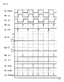
- FIG. 5 is a time chart in a case where the amplitude of the audio signal varies within a normal range.
- FIG. 6 is a time chart in a case where the amplitude of the audio signal varies within a positively-excessive range.
- FIG. 7 is a time chart in a case where the amplitude of the audio signal varies within a negatively-excessive range.
- FIG. 8 is a view illustrating an exemplary modification of a charging-current generation circuit.
- FIG. 9 is a block circuit diagram illustrating a second embodiment of the pulse width modulation circuit according to the present invention.
- FIG. 10 is a view illustrating a time chart for describing the operations of the pulse width modulation circuit according to the second embodiment.
- FIG. 11 is a circuit diagram illustrating a pulse width modulation circuit suggested by the present applicant.
- FIG. 12 is a timing chart illustrating the voltage waveforms of respective signals in the pulse width modulation circuit illustrated in FIG. 11 , illustrating a timing chart in the case where the audio signal is non signal.
- FIG. 13 is a timing chart illustrating the voltage waveforms of respective signals in the pulse width modulation circuit illustrated in FIG. 11 , illustrating a timing chart in the case where the audio signal is negatively excessive.
- FIG. 14 is a view illustrating the change of the voltage across a first capacitor at the time when the audio signal is restored from a state where it is negatively excessive to a normal state, at a state where the charging start voltage has decreased.
- FIG. 1 is a structure view of a switching amplifier to which a pulse width modulation (PWM) circuit according to the present invention is applied.
- FIG. 2 is a block circuit diagram illustrating a first embodiment of the pulse width modulation circuit illustrated in FIG. 1 .
- the switching amplifier includes a pulse width modulation circuit 1 connected to an audio-signal source AU, a switching circuit 2 , a low-pass filter circuit 3 , and a first power supply 4 and a second power supply 5 which supply positive and negative power-supply voltages +EB and ⁇ EB.
- a speaker (not illustrated), as a load RL, is connected to the output of the low-pass filter 3 .
- the pulse width modulation circuit 1 converts an audio signal e s as an input signal outputted from the audio-signal source AU into a pulse-width modulated signal PWMout and outputs it.
- the pulse-width modulated signal PWMout outputted from the pulse width modulation circuit 1 is inputted to the switching circuit 2 .
- the switching circuit 2 includes a switch device SW-A which is controlled in ON and OFF operations through the pulse-width modulated signal PWMout, an inverter 2 a which inverts the phase of the pulse-width modulated signal PWMout outputted from the pulse width modulation circuit 1 , a switch device SW-B which is controlled in ON and OFF operations through the pulse-width modulated signal PWMout′ with the inverted phase outputted from the inverter 2 a , and counter-current prevention diodes D-A and D-B which are connected to the opposite ends of the respective switch devices SW-A and SW-B.
- the positive and negative power-supply voltages +EB and ⁇ EB from the first power supply 4 and the second power supply 5 are supplied through the switch devices SW-A and SW-B to the load RL.
- the switch device SW-A and the switch device SW-B are alternately subjected to ON and OFF operations through the pulse-width modulated signal PWMout and the pulse-width modulated signal PWMout′ and, accordingly, the power-supply voltage +EB and the power-supply voltage ⁇ EB are alternately supplied to the low-pass filter circuit 3 and the load RL.
- the load RL is supplied, through the low-pass filter 3 , with a rectangular-wave voltage which is varied in level between +EB and ⁇ EB and has the same duty ratio as that of the pulse-width modulated signal PWMout.
- the low-pass filter circuit 3 is made up of an LC circuit having a coil L 0 and a capacitor C 0 .
- the low-pass filter circuit 3 is a circuit which eliminates high-frequency components from the rectangular-wave voltage inputted from the switching circuit 2 and has a cut-off frequency of 60 kHz, for example.
- the low-pass filter circuit 3 outputs an AC voltage signal (an AC voltage signal with substantially the same waveform as that of the audio signal e s ) resulted from the demodulation of the pulse-width modulated signal PWMout, and this AC voltage signal is supplied to the load RL, so that the audio signal e s is outputted as sounds.
- the pulse width modulation circuit 1 includes a reference-clock generation circuit 11 , a dead-time generation circuit 12 , a trailing-edge detection circuit 13 , a charging-current generation circuit 14 , first to fourth switches SW 1 to SW 4 , first and second capacitors C 1 and C 2 , a discharging constant-current source 15 , a current bypass circuit 16 , first and second RS flip flop circuits 17 and 18 , and a signal output circuit 19 , as illustrated in FIG. 2 .
- the pulse width modulation circuit 1 has basically the same structure as that of the pulse width modulation circuit 51 illustrated in FIG. 11 , as is apparent from the comparison between FIG. 2 and FIG. 11 .
- the reference-clock generation circuit 11 , the dead-time generation circuit 12 and the trailing-edge detection circuit 13 correspond to the reference-clock generation circuit 54 , the dead-time generation circuit 55 and the trailing-edge detection circuits 56 in the pulse width modulation circuit 51 .
- the charging-current generation circuit 14 , the constant-current source 15 and the current bypass circuit 16 correspond to the charging-current generation circuit 57 , the constant-current source 58 and the current bypass circuit 59 , respectively, in the pulse width modulation circuit 51 .
- first to fourth switches SW 1 to SW 4 and the first and second capacitors C 1 and C 2 correspond to the first to fourth switches SW 11 to SW 14 and the first and second capacitors C 11 and C 12 , respectively, in the pulse width modulation circuit 51 .
- the first and second RS flip flop circuits 17 and 18 and the signal output circuit 19 correspond to the first and second RS flip flop circuits 60 and 61 and the signal output circuit 62 , respectively, in the pulse width modulation circuit 51 .
- the pulse width modulation circuit 1 according to the first embodiment is different from the pulse width modulation circuit 51 , only in the circuit structure of the charging-current generation circuit 14 , and this different circuit structure is a characteristic point of the present invention. The characteristic point will be described, later.
- the pulse width modulation circuit 1 converts the audio signal e s into a pulse-width modulated signal PWMout, on the basis of the following operation principles.
- a charging current Ij for charging the first and second capacitors C 1 and C 2 is generated by the charging-current generation circuit 14 from the audio signal e s inputted from the outside.
- the first or second capacitor C 1 or C 2 is charged with the charging current Ij within each charging time interval, and the electric charge accumulated in the first or second capacitor C 1 or C 2 is discharged with a constant discharging current Id within each discharging time interval, assuming that the former half cycle and the latter half cycle, out of a single cycle of a reference clock MCLK, are a charging time interval and a discharging time interval, respectively, for the first capacitor C 1 , while the former half cycle and the latter half cycle are a discharging time interval and a charging time interval, respectively, for the second capacitor C 2 .
- a pulse signal with a pulse width equal to the discharging time interval required for changing the voltage across the first or second capacitor C 1 or C 2 to a predetermined threshold voltage Vth from the start of discharging (the end of charging) is generated.
- the pulse signals alternately generated during the respective half cycles of the reference clock MCLKA are synthesized to generate a pulse-width modulated signal PWMout.
- the reference-clock generation circuit 11 is a circuit which generates the aforementioned reference clock MCLK.
- the reference clock MCLK is a clock signal with a constant period and a duty ratio of about 50% and serves as a reference signal for first and second switching signals ⁇ 1 and ⁇ 2 for controlling the ON and OFF operations of the first and second switches SW 1 and SW 2 . Further, the reference clock MCLK serves as a reference signal for defining the period of the pulse-width modulated signal PWMout.
- the reference-clock generation circuit 11 outputs the reference clock MCLK to the dead-time generation circuit 12 . Also, the reference-clock generation circuit 11 can be provided outside of the pulse width modulation circuit 1 and can be structured to supply the reference clock MCLK as an external clock signal to the pulse width modulation circuit 1 .
- the dead-time generation circuit 12 is a circuit which generates a first switching signal ⁇ 1 and a second switching signal ⁇ 2 , on the basis of the reference clock MCLK from the reference-clock generation circuit 11 .
- the second switching signal ⁇ 1 has the opposite phase from that of the first switching signal ⁇ 2 , but the timing of the inversion of the level of the second switching signal ⁇ 2 is deviated by a predetermined time ⁇ T (a dead time) from the timing of the inversion of the level of the first switching signal ⁇ 1 , in order to prevent the timing of the trailing edges and the leading edges of the second switching signal ⁇ 2 from coinciding with the timing of the leading edges and the trailing edges of the first switching signal ⁇ 1 .
- the first switching signal ⁇ 1 is a signal which is inverted from a low level to a high level at timing delayed by the predetermined time ⁇ T from the timing when the reference clock MCLK is inverted from a low level to a high level and, also, is inverted from the high level to the low level at the same timing as the timing when the reference clock MCLK is inverted from the high level to the low level.
- FIGS. 5 and 6( a ) and ( b ) the first switching signal ⁇ 1 is a signal which is inverted from a low level to a high level at timing delayed by the predetermined time ⁇ T from the timing when the reference clock MCLK is inverted from a low level to a high level and, also, is inverted from the high level to the low level at the same timing as the timing when the reference clock MCLK is inverted from the high level to the low level.
- the second switching signal ⁇ 2 is a signal which is inverted from a high level to a low level at the same timing as the timing when the reference clock MCLK is inverted from the low level to the high level and, also, is inverted from the low level to the high level at timing delayed by the predetermined time ⁇ T from the timing when the reference clock MCLK is inverted from the low level to the high level.
- the inversion of the first switching signal ⁇ 1 into the high level and the inversion of the second switching signal ⁇ 2 into the low level do not occur at the same timing and, also, the inversion of the first switching signal ⁇ 1 into the low level and the inversion of the second switching signal ⁇ 2 into the high level do not occur at the same timing.
- the second switch SW 2 has been already changed over to an OFF state through the second switching signal ⁇ 2 (the charging-current generation circuit 14 has been already disconnected from the second capacitor C 1 ), which prevents the first and second capacitors C 1 and C 2 from being connected to the charging-current generation circuit 14 at the same time.
- the first switch SW 1 has been already changed over to an OFF state through the first switching signal ⁇ 1 (the charging-current generation circuit 14 has been already disconnected from the first capacitor C 1 ), which prevents the first and second capacitors C 1 and C 2 from being connected to the charging-current generation circuit 14 at the same time.
- the charging current Ij being supplied to the first capacitor C 1 from the charging-current generation circuit 14 is prevented from being also supplied to the second capacitor C 2 during charging the first capacitor C 1 . Further, the charging current Ij being supplied to the second capacitor C 2 from the charging-current generation circuit 14 is prevented from being also supplied to the first capacitor C 1 during charging the second capacitor C 2 .
- This can prevent inconvenience of the occurrence of errors in the pulse width of the pulse width modulated signal PWMout, due to the occurrence of errors in the pulse widths of pulse signals outputted from the first and second RS flip flop circuits 17 and 18 .
- the first and second switching signals ⁇ 1 and ⁇ 2 are outputted to the first and second switches SW 1 and SW 2 and, also, are outputted to the trailing-edge detection circuit 13 .
- the dead time provided by the dead-time generation circuit 12 is an extremely short time interval and, therefore, it can be said that the switch SW 1 is controlled in ON and OFF substantially through the reference clock MCLK, and the second switch SW 2 is controlled in ON and OFF substantially through the clock with the opposite phase from that of the reference clock MCLK.
- the trailing-edge detection circuit 13 is a circuit which outputs first and second set signals set 1 and set 2 to be supplied to the first and second RS flip flop circuits 17 and 18 , which will be described later. Namely, the trailing-edge detection circuit 13 detects the timing when the first switching signal ⁇ 1 descends from the high level to the low level and outputs a signal which momentarily descends to a low level at the detected timing, as a first set signal set 1 , to the first RS flip flop circuit 17 , as illustrated in FIGS. 5 and 6( d ).
- the trailing-edge detection circuit 13 detects the timing when the second switching signal ⁇ 2 descends from the high level to the low level and outputs a signal which momentarily descends to a low level at the detected timing, as a second set signal set 1 , to the second RS flip flop circuit 18 , as illustrated in FIGS. 5 and 6( e ).
- the charging-current generation circuit 14 is a circuit which performs voltage-to-current conversion on the audio signal e s supplied to the pulse width modulation circuit 1 from the audio-signal source AU and adds a supplemental current Imin to the current IS resulted from the conversion to generate a charging current Ij.
- the charging-current generation circuit 14 is connected to the first and second capacitors C 1 and C 2 through the first and second switches SW 1 and SW 2 , as will be described later.
- the charging-current generation circuit 14 When the first switch SW 1 is at an ON state, the charging-current generation circuit 14 is connected to the first capacitor C 1 to charge the first capacitor C 1 with the charging current Ij and, when the second switch SW 2 is at an ON state, the charging-current generation circuit 14 is connected to the second capacitor C 2 to charge the second capacitor C 2 with the charging current Ij.
- the charging-current generation circuit 14 includes a voltage-to-current conversion portion 14 a and a supplemental-current generation portion 14 b .
- the pulse width modulation circuit 1 according to the first embodiment has a characteristic structure, in that it includes the additional-current generation portion 14 b.
- the voltage-to-current conversion portion 14 a is a circuit which includes a non-inverting input type voltage-to-current conversion circuit using mainly an OP amplifier 21 and converts the AC voltage signal as the audio signal e s into an electric current signal.
- the negative input terminal of the OP amplifier 21 is grounded through a resistance device R 3 and, also, is connected to the output terminal through a resistance device R 1 . Further, the negative input terminal of the OP amplifier 21 is connected to a negative power supply [ ⁇ Vcc] to generate a bias voltage for the OP amplifier 21 . Due to the bias voltage, at a no-input state (a state where the audio signal e s has an amplitude of 0), the OP amplifier 21 outputs a DC bias current Ic.
- the OP amplifier 21 is connected, at its output terminal, to the emitter terminal of a PNP-type transistor Q, through a diode D 1 and a resistance device R 5 . Further, the transistor Q is connected at its collector terminal to the first switch SW 1 and the second switch SW 2 and is supplied, at its base, with a bias voltage V 1 from a voltage source 22 .
- FIG. 3 is a view illustrating the relationship between the audio signal e s inputted to the OP amplifier 21 and the output current IS.
- the OP amplifier 21 outputs no electric current, regardless of the variation.
- the supplemental-current generation portion 14 b generates a supplemental current Imin and includes a diode D 1 , a positive power supply [+Vcc] and a resistance device R 4 .
- the diode D 1 is connected between the output terminal of the OP amplifier 21 and the resistance device R 5 , such that its anode is closer to the OP amplifier 21 .
- the resistance device R 4 is connected between the power supply [+Vcc] and the cathode of the diode D 1 .
- the charging current Ij becomes “0” and, accordingly, for example, even when the charging-current generation circuit 57 is connected to the first capacitor C 11 during a charging time interval, the first capacitor C 11 is not charged substantially, and the voltage across the first capacitor C 11 does not rise from the charging start voltage Va. Further, if this state continues over several cycles to several tens of cycles of the reference clock MCLK, this will induce the problem of stepwise decreases of the charging start voltage across the first capacitor C 11 . This fact also applies to the second capacitor C 12 .
- the charging start voltage Va is decreased in a stepwise manner, since the following operations are performed for, for example, the first capacitor C 11 . Namely, since the charging current Ij becomes “0” during each charging time interval, substantially no electric charge is accumulated in the first capacitor C 11 (the voltage across the first capacitor C 11 does not rise) during each charging time interval and, therefore, the charging end voltage Vc becomes equal to the charging start voltage Va.
- the charging start voltage is lower than the threshold voltage Vth, which maintains, at the low level, the input terminal of the first RS flip flop circuit 60 to which a first reset signal res 1 is inputted.
- the supplemental current Imin is supplied from the supplemental-current generation portion 14 b from the aforementioned perspective, and the magnitude of the supplemental current Imin is determined according to the following equation (1).
- Imin ⁇ ⁇ ⁇ t T ⁇ Id ( 1 )
- the equation (1) is determined as follows. Namely, the amount of electric charge accumulated in the first or second capacitor C 1 or C 2 during a charging time interval T is expressed as the following equation (2), assuming that the charging time interval is T, the discharging current supplied from the constant-current source 15 is Id, the time period during which momentary discharging from Vth to Va at the end of charging occurs is ⁇ t, the voltage difference between the charging start voltage Va and the threshold voltage Vth is ⁇ v, and the capacitance of the first or second capacitor C 1 or C 2 is C, as illustrated in FIG. 4 .
- ⁇ t means the short lag time period from the timing when the voltage across the first or second capacitor C 1 or C 2 has decreased to the threshold voltage Vth to the timing when the third or fourth switch SW 3 or SW 4 separates the constant-current source 15 since the third or fourth switching signal ⁇ 3 or ⁇ 4 is inverted to the low level, after the voltage across the first or second capacitor C 1 or C 2 has decreased to the threshold voltage Vth.
- the amount ⁇ Q of electric charge is equal to the amount Id* ⁇ t of electric charge discharged from the first or second capacitor C 1 or C 2 during the discharging time interval ⁇ t and, therefore, the following equation (3) holds, and the equation (1) is obtained by deforming the equation (3).
- I min ⁇ T Id ⁇ t (3)
- the magnitude of the supplemental current Imin is determined according to the equation (1), and is adjusted by the resistance value of the resistance device R 4 in the supplemental-current generation portion 14 b.
- the aforementioned inconvenience can be overcome when the supplemental current Imin is equal to or more than the value determined according to the equation (1).
- the value of the supplemental current is increased, this will narrow the range of the charging current Ij outputted from the charging-current generation circuit 14 , since the supplemental current is flowed by being included in the charging current Ij.
- the range of the charging current Ij outputted from the charging-current generation circuit 14 is a range equal to or more than 0 as illustrated by A′ in FIG. 3( b ).
- the supplemental current Imin is set to a minimum value, out of possible current values.
- the diode D 1 is brought into an OFF state. Accordingly, when the amplitude of the audio signal e s varies within the voltage range A of FIG. 3( a ), the output current IS from the OP amplifier 21 is larger than “0” and, therefore, the diode D 1 is at an ON state, which causes the charging-current generation circuit 14 to output a charging current Ij generated by adding the supplemental current Imin to the current resulted from the conversion (Ic ⁇ i).
- the charging current Ij supplied from the charging-current generation circuit 14 is varied with the amplitude of the audio signal e s , and the range of the change thereof is a range equal to or larger than Imin, which prevents the charging current Ij from being lower than Imin.
- the diode D 1 electrically separates the voltage-to-current conversion portion 14 a.
- the constant-current source 15 is for discharging the electric charge accumulated in the first or second capacitor C 1 or C 2 toward the negative power supply [ ⁇ Vcc] with the discharging current Id which is a constant current. Namely, as will be described later, the constant-current source 15 is connected to the first or second capacitor C 1 or C 2 through the third or fourth switch SW 3 or SW 4 , respectively. If the switch SW 3 is subjected to an ON operation so that the constant-current source 15 is connected to the first capacitor C 1 , the electric charge accumulated in the first capacitor C 1 is discharged toward the negative power supply [ ⁇ Vcc] with the discharging current Id.
- the current bypass circuit 16 includes a diode D 2 and a voltage source 23 .
- the current bypass circuit 16 is for flowing a discharge current Id even when the constant-current source 15 is not electrically connected to the first or second capacitors C 1 or C 2 through the third or fourth switches SW 3 or SW 4 . Namely, when the constant-current source 15 is not electrically connected to the first or second capacitor C 1 or C 2 through the third or fourth switch SW 3 or SW 4 , the diode D 2 is at an ON state, and the voltage source 23 is connected to the constant-current source 15 .
- the voltage at the cathode side of the diode D 2 is higher than the negative power supply [ ⁇ Vcc] and, therefore, a discharging current Id flows toward the negative power supply [ ⁇ Vcc] through the diode D 2 from the voltage source 23 .
- the third switch SW 3 is turned on to connect the first capacitor C 1 to the constant-current source 15 , since the voltage across the first capacitor C 1 is higher than the voltage at the cathode side of the diode D 2 , the diode D 2 is brought into an OFF state, thereby changing over the flow path for the flow of the discharging current Id, from the voltage source 23 to the first capacitor C 1 .
- the operation for discharging the electric charge accumulated in the first capacitor C 1 with the discharging current Id is started.
- the same operation is performed when the fourth switch SW 4 is turned on and, at the same timing as the timing when the fourth switch SW 4 is turned on, the operation for discharging the electric charge accumulated in the second capacitor C 2 with the discharging current Id is started.
- the first and second switches SW 1 and SW 2 are switches for controlling the operation for charging the first and second capacitors C 1 and C 2 with the charging current Ij from the charging-current generation circuit 14 .
- the first switch SW 1 is connected at its one end to the output end of the charging-current generation circuit 14 (the collector terminal of the transistor Q) and also is connected at the other end to one end of the first capacitor (see the point A in FIG. 2 ).
- the first switch SW 1 is subjected to an ON operation (when it is brought into a closed state), a path for charging the first capacitor C 1 is formed.
- the second switch SW 2 is connected at its one end to the output end of the charging-current generation circuit 14 (the collector terminal of the transistor Q) and also is connected at the other end to one end of the second capacitor (see the point A′ in FIG. 2 ).
- the second switch SW 2 is subjected to an ON operation (when it is brought into a closed state), a path for charging the first capacitor C 2 is formed.
- the ON and OFF operations of the first and second switches SW 1 and SW 2 are performed through the first and second switching signals ⁇ 1 and ⁇ 2 which are outputted from the dead-time generation circuit 12 . Namely, an ON operation is performed on the first switch SW 1 when the first switching signal ⁇ 1 is at the high level, while an OFF operation is performed thereon when the first switching signal ⁇ 1 is at the low level, as illustrated in FIG. 5 and FIG. 6( b ). Further, an ON operation is performed on the second switch SW 2 when the second switching signal ⁇ 2 is at the high level, while an OFF operation is performed thereon when the second switching signal ⁇ 2 is at the low level, as illustrated in FIG. 5 and FIG. 6( c ).
- the third and fourth switches SW 3 and SW 4 are switches for controlling the operation for discharging the first and second capacitors C 1 and C 2 with the discharging current Id from the constant-current source 15 .
- the third switch SW 3 is connected at its one end to the constant-current source 15 and also is connected at the other end to one end of the first capacitor (see the point A in FIG. 2 ).
- the third switch SW 3 is subjected to an ON operation (when it is brought into a closed state)
- a path for discharging the first capacitor C 1 is formed.
- the fourth switch SW 4 is connected at its one end to the constant-current source 15 and also is connected at the other end to one end of the second capacitor (see the point A′ in FIG. 2 ).
- the fourth switch SW 4 is subjected to an ON operation (when it is brought into a closed state)
- a path for discharging the second capacitor C 2 is formed.
- the ON and OFF operations of the third and fourth switches SW 3 and SW 4 are performed through the third and fourth switching signals ⁇ 3 and ⁇ 4 which are outputted from the first and second RS flip flop circuits 17 and 18 .
- an ON operation is performed on the third switch SW 3 when the third switching signal ⁇ 3 is at the high level, while an OFF operation is performed thereon when the third switching signal ⁇ 3 is at the low level, as illustrated in FIG. 5 and FIG. 6( h ).
- an ON operation is performed on the fourth switch SW 4 when the fourth switching signal ⁇ 4 is at the high level, while an OFF operation is performed thereon when the fourth switching signal ⁇ 4 is at the low level, as illustrated in FIG. 5 and FIG. 6( i ).
- the first and second capacitors C 1 and C 2 are for generating a time interval corresponding to the amplitude (the momentary voltage value) of the audio signal e s . More specifically, during the ON time interval (a constant time interval) of the first switching signal ⁇ 1 , an ON operation is performed on the first switch SW 1 (at this time, an OFF operation is performed on the third switch SW 3 ).
- an ON operation is performed on the third switch SW 3 (at this time, an OFF operation is performed on the first switch SW 1 ), which causes the accumulated electric charge to be discharged with the constant discharging current Id.
- the discharging time interval required for decreasing the voltage across the first capacitor C 1 from the charging end voltage Vc to the predetermined threshold voltage Vth is generated as a time interval corresponding to the amplitude (the momentary voltage value) of the audio signal e s .
- the predetermined threshold voltage Vth is a threshold voltage for the logic levels of the first and second RS flip flop circuits 17 and 18 and is a voltage equal to about 1 ⁇ 2 the power supply voltage +Vcc supplied to the first and second RS flip flop circuits 17 and 18 .
- the threshold voltage Vth is about +2.5 [v].
- the charging start voltage Va is a voltage slightly lower than the threshold voltage Vth.
- An ON operation is performed on the third switch SW 3 during the ON time interval (a constant time interval) of the third switching signal ⁇ 3 (at this time, an OFF operation is performed on the fourth switch SW 4 ).
- the third switch is turned on, the second capacitor C 2 is charged with the charging current Ij from the charging-current generation circuit 14 , and the voltage across the second capacitor C 2 is raised from the charging start voltage Va to the voltage Vc corresponding to the amplitude of the audio signal e s (the charging end voltage).
- an ON operation is performed on the fourth switch SW 4 (at this time, an OFF operation is performed on the second switch SW 2 ), which causes the accumulated electric charge to be discharged with the constant discharging current Id.
- the discharging time interval required for decreasing the voltage across the second capacitor C 2 from the charging end voltage Vc to the predetermined threshold voltage Vth is generated as a time interval corresponding to the amplitude (the momentary voltage value) of the audio signal e s .
- the first RS flip flop circuit 17 is a circuit which, during each discharging time interval for the first capacitor C 1 , generates a pulse signal with a pulse width equal to the discharging time interval for the first capacitor C 1 and, also, generates a third switching signal ⁇ 3 .
- the first RS flip flop circuit 17 is an RS flip flop circuit having two NAND gates (a first NAND circuit NA 1 and a second NAND circuit NA 2 ).
- the voltage across the first capacitor C 1 is inputted as a first reset signal res 1 to the first NAND circuit NA 1 , and the first NAND circuit NA 1 outputs an output rsout 1 .
- a first set signal set 1 (a signal which momentarily descends to a level lower than the threshold voltage Vth) outputted from the trailing-edge detection circuit 13 is inputted to the second NAND circuit NA 2 , and the second NAND circuit NA 2 outputs a third switching signal ⁇ 3 .
- the first RS flip flop circuit 17 If the first set signal set 1 is inputted to the first RS flip flop circuit 17 , the first RS flip flop circuit 17 inverts the output rsout 1 to the low level and, also, inverts the third switching signal ⁇ 3 to the high level. If the voltage across the first capacitor C 1 is brought into a low level (equal to or lower than the threshold voltage Vth), namely if a first reset signal res 1 is inputted thereto, the first RS flip flop circuit 17 inverts the output rsout 1 to the high level and, also, inverts the third switching signal ⁇ 3 to the low level.
- Vth threshold voltage
- the timing of the input of the first set signal set 1 corresponds to the timing when the discharging of the first capacitor C 1 is started, and the timing of the input of the first reset signal res 1 corresponds to the timing when the voltage across the first capacitor C 1 has decreased to the threshold voltage vth and, accordingly, the time interval during which the output rsout 1 is at the low level corresponds to the time interval during which the first capacitor C 1 is discharged.
- the first NAND circuit NA 1 in the first RS flip flop circuit 17 outputs, from its output terminal, a pulse signal with a pulse width equal to the discharging time interval for the first capacitor C 1 , as an output rsout 1 .
- the second RS flip flop circuit 18 is a circuit which, during each discharging time interval for the second capacitor C 2 , generates a pulse signal with a pulse width equal to the discharging time interval for the second capacitor C 2 and generates a fourth switching signal ⁇ 4 .
- the second RS flip flop circuit 18 is an RS flip flop circuit having two NAND gates (a third NAND circuit NA 3 and a fourth NAND circuit NA 4 ).
- the voltage across the second capacitor C 2 is inputted as a second reset signal res 2 to the third NAND circuit NA 3 , and the third NAND circuit NA 3 outputs an output rsout 2 .
- a second set signal set 2 (a signal which momentarily descends to a level lower than the threshold voltage Vth) outputted from the trailing-edge detection circuit 13 is inputted to the fourth NAND circuit NA 4 , and the fourth NAND circuit NA 4 outputs a fourth switching signal ⁇ 4 .
- the second RS flip flop circuit 18 If the second set signal set 2 is inputted to the second RS flip flop circuit 18 , the second RS flip flop circuit 18 inverts the output rsout 1 to the low level and, also, inverts the fourth switching signal ⁇ 4 to the high level. If the voltage across the second capacitor C 2 is brought into a low level (equal to or lower than the threshold voltage Vth), namely if the second reset signal res 2 is inputted thereto, the second RS flip flop circuit 18 inverts the output rsout 2 to the high level and, also, inverts the fourth switching signal ⁇ 4 to the low level.
- Vth threshold voltage
- the timing of the input of the second set signal set 2 corresponds to the timing when the discharging of the second capacitor C 2 is started, and the timing of the input of the second reset signal res 2 corresponds to the timing when the voltage across the second capacitor C 2 has decreased to the threshold voltage vth and, accordingly, the time interval during which the output rsout 2 is at the low level corresponds to the time interval during which the second capacitor C 2 is discharged.
- the third NAND circuit NA 3 in the second RS flip flop circuit 18 outputs, from its output terminal, a pulse signal with a pulse width equal to the discharging time interval for the second capacitor C 2 , as an output rsout 2 .
- the signal output circuit 19 is a circuit which synthesizes the output rsout 1 outputted from the first RS flip flop circuit 17 and the output rsout 2 outputted from the second RS flip flop circuit 18 .
- the signal output circuit 19 is made up of a NAND gate (a fifth NAND circuit NA 5 ).
- the rsout 1 is a signal which has pulse signals (pulse signals with a pulse width equal to a discharging time interval for the first capacitor C 1 ) during the time intervals during which the reference clock MCLK is at the low level
- the rsout 2 is a signal which has pulse signals (pulse signals with a pulse width equal to a discharging time interval for the second capacitor C 2 ) during the time intervals during which the reference clock MCLK is at the high level.
- the signal output circuit 19 outputs, as a pulse width modulated signal PWMout, pulse signals generated by alternately combining the pulse signals of the output rsout 1 and the pulse signals of the output rsout 2 (a signal having a series of pulses with a pulse width corresponding to the amplitude (the momentary voltage value) of the audio signal eS with a period equal to the half the period of the reference clock MCLK).
- FIG. 5 is a time chart in the case where the amplitude of the audio signal e s varies within a normal range (the range from ⁇ Es to +Es).
- the high-level time intervals and the low-level time intervals of the first switching signal ⁇ 1 correspond to the charging time intervals and the discharging time intervals for the first capacitor C 1 , respectively. If the first switching signal ⁇ 1 is inverted to the high level, this causes the first switch SW 1 to connect the charging-current generation circuit 14 to the first capacitor C 1 , thereby starting charging the first capacitor C 1 with the charging current Ij from the charging-current generation circuit 14 . This charging operation is continued until the first switching signal ⁇ 1 is inverted to the low level and the first switch SW 1 separates the charging-current generation circuit 14 (see FIGS. 5 ( b ) and ( f )).
- a first set signal set 1 resulted from the detection of this inversion to the low level causes the third switching signal ⁇ 3 outputted from the first RS flip flop circuit 17 to be inverted to the high level, which causes the third switch SW 3 to connect the constant-current source 15 to the first capacitor C 1 , thereby starting discharging the first capacitor C 1 with the discharging current Id from the constant-current source 15 .
- the first RS flip flop circuit 17 outputs, as an output rsout 1 , a pulse signal which is inverted to the low level at the same timing as the timing when a first set signal set 1 is inputted thereto and, then, is inverted to the high level at the same timing as the timing when the voltage across the first capacitor C 1 , which is inputted as the first reset signal res 1 thereto, has decreased to the threshold voltage Vth.
- a pulse signal with a pulse width corresponding to the amplitude (the momentary voltage value) of the audio signal e s is generated (see FIG. 5 ( j )).
- the high-level time intervals and the low-level time intervals of the second switching signal ⁇ 2 correspond to the charging time intervals and the discharging time intervals for the second capacitor C 2 , respectively. If the dead time is neglected, the second switching signal ⁇ 2 is the same signal as the first switching signal ⁇ 1 but has the opposite phase therefrom and, accordingly, the same charging and discharging operations as the charging and discharging operations for the first capacitor C 1 are performed for the second capacitor C 2 , such that they are deviated by the half the period of the first switching signal ⁇ 1 (see FIGS. 5 ( c ), ( e ), ( g ) and ( i )).
- the second RS flip flop circuit 18 outputs, as an output rsout 2 , a pulse signal which is inverted to the low level at the same timing as the timing when a second set signal set 2 is inputted thereto and, then, is inverted to the high level at the same timing as the timing when the voltage across the second capacitor C 2 , which is inputted as the second reset signal res 2 thereto, has decreased to the threshold voltage Vth.
- a pulse signal with a pulse width corresponding to the amplitude (the momentary voltage value) of the audio signal e s is generated (see FIG. 5 ( k )).
- the signal output circuit 19 synthesizes the output rsout 1 and the output rsout 2 outputted from the first and second flip flop circuits 17 and 18 and output the signal resulted from the synthesis, as a pulse-width modulated signal PWMout (a signal generated by synthesizing the waveform of the output rsout 1 and the waveform of the output rsout 2 ) (see FIG. 5( l )).
- PWMout a signal generated by synthesizing the waveform of the output rsout 1 and the waveform of the output rsout 2
- the voltage across the first or second capacitor C 1 or C 2 is certainly raised to the charging end voltage Vc which is higher than the threshold voltage Vth during each charging time interval. Accordingly, even after the transition to the discharging time interval, the voltage across the first or second capacitor C 1 or C 2 normally becomes the charging start voltage Va, which causes the voltage across the first or second capacitor C 1 or C 2 to be certainly maintained at the charging start voltage Va after the discharging is stopped. This can stabilize, at Va, the charging start voltage across the first or second capacitor C 1 or C 2 , in each charging time interval (see FIGS. 5 ( f ) and ( g )).
- FIG. 6 is a time chart in the case where the amplitude of the audio signal e s varies within a positively-excessive range (a range equal to or larger than +Es).
- the processing for generating a pulse-width modulated signal PWMout in the case where the amplitude of the audio signal e s varies within a positively-excessive range (a range equal to or larger than +Es) is not different from that in the case where the amplitude of the audio signal e s varies within the normal range (the range from ⁇ Es to +Es) and, therefore, will not be described in detail, and only the different points will be described.
- the charging current Ij varies with the amplitude of the audio signal e s and, accordingly, the waveforms of the voltages across the first and second capacitors C 1 and C 2 illustrated in FIGS. 5 ( f ) and ( g ) vary with the amplitude of the audio signal e s . More specifically, the charging end voltage Vc to which the voltages across the first and second capacitors C 1 and C 2 are raised during the charging time intervals is varied within the range of Vth (>0) to Vcc, according to the amplitude of the audio signal e s .
- the waveform of the voltage across the first capacitor C 1 varies within the range sandwiched between the voltage waveform illustrated by a chain line N 1 and the waveform illustrated by a dotted line N 2 . This also applies to the waveform of the voltage across the second capacitor C 2 .
- the charging end voltage Vc across the first and second capacitors C 1 and C 2 is clipped to the power-supply voltage +Vcc for the first and second RS flip flop circuits 17 and 18 . Accordingly, as illustrated in FIGS. 6 ( f ) and ( g ), the waveforms during discharging the first and second capacitors C 1 and C 2 are the same as the waveform during discharging, out of the voltage waveform illustrated by the chain line N 1 in FIG. 5 ( f ).
- the voltage across the first or second capacitor C 1 or C 2 is certainly raised to the charging end voltage Vc which is higher than the threshold voltage Vth, during each charging time intervals. Even after the transition to the discharging time interval, the voltage across the first or second capacitor C 1 or C 2 normally becomes the charging start voltage Va. Accordingly, the voltage across the first or second capacitor C 1 or C 2 can be certainly maintained at the charging start voltage Va after the stop of discharging. This can stabilize, at Va, the charging start voltage across the first or second capacitor C 1 or C 2 , in each charging time interval (see FIGS. 6 ( f ) and ( g )).
- FIG. 7 is a time chart in the case where the amplitude of the audio signal e s varies within a negatively-excessive range (a range equal to or smaller than ⁇ Es).
- the processing for generating a pulse-width modulated signal PWMout in the case where the amplitude of the audio signal e s varies within a negatively-excessive range (a range equal to or smaller than ⁇ Es) is not different from that in the case where the amplitude of the audio signal e s varies within the normal range (the range of ⁇ Es to +Es) and, therefore, will not be described in detail, and only the different points will be described.
- the charging current Ij is clipped to Imin regardless of the amplitude ⁇ E of the audio signal e s . Accordingly, as illustrated in FIGS. 7 ( f ) and ( g ), the waveforms of the voltages across the first and second capacitors C 1 and C 2 are the same as the voltage waveform illustrated by the dotted line N 2 in FIGS. 5 ( f ) and ( g ).
- the first and second capacitors C 1 and C 2 are certainly charged with the supplemental current Imin until the voltages across them are raised to equal to or higher than the threshold voltage Vth, during the charging time intervals. Accordingly, even though the voltage across the first or second capacitor C 1 or C 2 decreases during the time lag ⁇ t which occurs at the time of the transition to each discharging time interval, the voltages across the first and second capacitors C 1 and C 2 are prevented from decreasing to below the charging start voltage Va.
- the pulse width modulation circuit 1 when the amplitude of the audio signal e s is brought into a negatively-excessive range (a range equal to or smaller than ⁇ Es), the charging current Ij supplied from the charging-current generation circuit 14 is fixed to the supplemental current Imin, which can prevent the voltages across the first and second capacitors C 1 and C 2 at the start of charging in each charging time interval from varying from the reference charging start voltage Va.
- the charging start voltage Va across the first and second capacitors C 1 and C 2 is stabilized. Accordingly, if the amplitude of the audio signal e s is restored to within the normal range, it is possible to immediately output a PWM modulated signal PWMout with a pulse width corresponding to the amplitude. Therefore, even if the amplitude of the audio signal e s is suddenly changed to within the normal range from within the negatively-excessive range, it is possible to normally reproduce the audio signal e s at the time of the occurrence of the sudden change, without inducing distortions.
- the circuit for flowing the supplemental current Imin is provided inside the charging-current generation circuit 14 , for example, as illustrated in FIG. 8 , the supplemental-current generation portion 14 b can be eliminated from the charging-current generation circuit 14 , and a constant current source 23 can be connected to the collector terminal (the output terminal) of the transistor Q, such that the supplemental current Imin from the constant current source 23 can be flowed toward the first and second switches SW 1 and SW 2 .
- the charging current Ij equals to Imin, and the charging current Ij supplied to the first or second capacitor C 1 or C 2 is substantially the same as that in the first embodiment.
- the transistor Q prevents the supplemental current Imin from flowing toward the voltage-to-current conversion portion 14 a , which eliminates the necessity of providing a diode for counter-current prevention, as illustrated in FIG. 2 .
- FIG. 9 is a block circuit diagram illustrating a second embodiment of the pulse width modulation circuit. Further, in FIG. 9 , there are illustrated only the portions different from FIG. 2 , and the reference clock generation circuit 11 , the dead-time generation circuit 12 , the trailing-edge circuit 13 , the first RS flip flop circuit 17 , the second RS flip flop circuit 18 , and the signal output circuit 19 are not illustrated.
- FIG. 10 is a time chart illustrating operations of the pulse width modulation circuit 1 ′ according to the second embodiment. Further, in FIG. 10 , there is mainly illustrated a time chart regarding signals relating to the first capacitor C 1 , but the time chart regarding the second set signal set 2 , the voltage across the second capacitor C 2 during charging and discharging, the fourth switching signal ⁇ 4 , and the output rsout 2 are not illustrated.
- the direction of the changes of the voltages across the first and second capacitors C 1 and C 2 during the charging and discharging time intervals is made opposite from that in the first embodiment. Namely, while, in the first embodiment, the voltages across the first and second capacitors C 1 and C 2 are raised from the charging start voltage Va (for example, a voltage slightly lower than the threshold voltage Vth) to the charging end voltage Vc (for example, a voltage in the range of +2.5 to +5.0 [v]) during the charging time intervals, and the voltages across the first and second capacitors C 1 and C 2 are decreased from the charging end voltage Vc to the threshold voltage Vth (for example, a voltage of +2.5 [v]) during the discharging time intervals, in the second embodiment, the voltages across the first and second capacitors C 1 and C 2 are decreased from a charging start voltage Vb (for example, a voltage slightly higher than a voltage reference voltage Vref) to a charging end voltage Vc (for example, a voltage in the range of ⁇ 5.0 to
- the pulse width modulation circuit 1 ′ according to the second embodiment is different from the pulse width modulation circuit 1 according to the first embodiment, in that the charging-current generation circuit 14 , the constant current source 15 for discharging and the current bypass circuit 16 are changed to a discharging-current generation circuit 24 , a constant current source 25 for charging, and a current bypass circuit 26 and, also, a first voltage comparator 27 and a second voltage comparator 28 are added between the first capacitor C 1 and the first RS flip flop circuit 17 and between the second capacitor C 2 and the second RS flip flop circuit 18 , respectively.
- the current Ih generated by the discharging-current generation circuit 24 is the same as the charging current Ij generated by the charging-current generation circuit 14 , but the direction of the current Ih is opposite from that of the charging current Ij. Namely, the discharging-current generation circuit 24 adds the supplemental current Imin to a current IS varying with the amplitude E of the audio signal e s to generate the discharging current Ih, and the discharging current Ih flows in the direction from the first switch SW 1 toward the discharging-current generation circuit 24 . Accordingly, the electric charge accumulated in the first capacitor C 1 is discharged with the discharging current Ih during a time interval during which the first switch SW 1 is ON (a time interval during which the first switching signal ⁇ 1 is at the high level).
- the discharging-current generation circuit 24 also includes a voltage-to-current conversion portion 24 a and a supplemental-current generation circuit 24 b , but the direction of the output current is opposite and, therefore, the voltage-to-current conversion portion 24 a is constituted by an inverting-input type voltage-to-current conversion circuit which employs an OP amplifier 21 .
- the positive-side input terminal of the OP amplifier 21 is connected to the audio-signal source AU through a resistance device R 3 and, also, is connected to the output terminal through a resistance device R 1 .
- the positive-side input terminal of the OP amplifier 21 is connected to the positive power supply [+Vcc] through a resistance device R 2 to generate a bias voltage for the OP amplifier 21 . Further, the OP amplifier 21 is grounded at its negative-side input terminal.
- the transistor Q is constituted by an NPN-type transistor and is connected at its emitter terminal to the output terminal of the OP amplifier 21 through a diode D 1 and a resistance device R 5 . Further, the transistor Q is connected at its collector terminal to the switch SW 1 and the switch SW 2 and is supplied at its base with a negative bias voltage V 1 from the voltage supply 22 .
- the supplemental-current generation portion 24 b basically has the same structure as that of the supplemental-current generation portion 14 b , but the direction of the flow of the supplemental current Imin is opposite therefrom and, therefore, the power supply has a value of [ ⁇ Vcc] and, also, the direction of the connection of the diode D 1 is opposite therefrom.
- the charging constant current source 25 is different from the discharging constant current source 15 , only in that it is connected to the positive power supply [+Vcc], and a constant current Id is flowed from the power supply [+Vcc] toward the first and second switches SW 1 and SW 2 .
- the charging current bypass circuit 26 is different from the charging current bypass circuit 16 , in that the polarities of the voltage source 23 and the diode D 2 are opposite therefrom.
- the current Id′ (hereinafter, referred to as the “discharging current Id′) from the constant current source 25 flows toward the current bypass circuit 26 .
- the third switch SW 3 is brought into an ON state
- the discharging current Id′ is supplied to the first capacitor C 1 through the third switch SW 3 .
- the fourth switch SW 4 is OFF
- the current Id′ from the constant current source 25 flows toward the current bypass circuit 26 .
- the fourth switch SW 4 is brought into an ON state, the discharging current Id′ is supplied to the second capacitor C 2 through the fourth switch SW 4 .
- the time intervals during which the first switching signal ⁇ 1 is ON are time intervals during which the first capacitor C 1 is discharged, while the time intervals during which the second switching signal ⁇ 2 is ON are time intervals during which the second capacitor C 2 is discharged. Further, the time intervals during which the first switching signal ⁇ 1 is OFF are time intervals during which the first capacitor C 1 is charged, while the time intervals during which the second switching signal ⁇ 2 is OFF are time intervals during which the second capacitor C 2 is charged.
- the first voltage comparator 27 detects the timing when the voltage across the first capacitor C 1 has risen from the discharging start voltage Vc′ to the reference voltage Vref and inputs a signal indicative of the detection, as a first rest signal res 1 , to the first RS flip flop circuit 17 .
- the reference voltage Vref is inputted to the positive input terminal of the first voltage comparator 27 , while the voltage across the first capacitor C 1 is inputted to the negative input terminal thereof.
- the first voltage comparator 27 outputs, from its output terminal, a signal which is brought into a low level if the voltage across the capacitor C 1 exceeds the reference voltage Vref and is brought into a high level if the voltage across the capacitor C 1 decreases to below the reference voltage Vref.
- the signal outputted from the first voltage comparator 27 is inputted to the first RS flip flop circuit 17 and, out of this signal, the signals indicative of the inversion from the high level to the low level become first reset signals res 1 for the first RS flip flop circuit 17 .
- the second voltage comparator 28 detects the timing when the voltage across the second capacitor C 2 has risen from the discharging start voltage Vc′ to the reference voltage Vref and inputs a signal indicative of the detection, as a second rest signal res 2 , to the second RS flip flop circuit 18 .
- the reference voltage Vref is inputted to the positive input terminal of the second voltage comparator 28 , while the voltage across the second capacitor C 2 is inputted to the negative input terminal thereof.
- the second voltage comparator 28 outputs, from its output terminal, a signal which is brought into a low level if the voltage across the second capacitor C 2 exceeds the reference voltage Vref and is brought into a low level if the voltage across the second capacitor C 1 decreases to below the reference voltage Vref.
- the signal outputted from the second voltage comparator 28 is inputted to the second RS flip flop circuit 18 and, out of this signal, the signals indicative of the inversion from the high level to the low level become second reset signals res 2 for the second RS flip flop circuit 18 .
- the reference voltage Vref in the first and second voltage comparators 27 and 28 functions as a voltage for determining the discharging time interval for the first and second capacitors C 1 and C 2 and corresponds to the threshold voltage Vth according to the first embodiment.
- the second embodiment similarly to in the first embodiment, there is a time lag from the timing when the third or fourth switching signal ⁇ 3 or ⁇ 4 is inverted to the high level to the timing when the third or fourth switch SW 3 or SW 4 is actually turned off. Accordingly, the charging operation with the charging current Id′ is continued during the time lag period, which raises the voltage across the first or second capacitor C 1 or C 2 to the voltage Vb which is slightly higher than the reference voltage Vref. This voltage Vb becomes the discharging start voltage at the next discharging start time interval.
- the pulse width modulation circuit 1 ′ With the pulse width modulation circuit 1 ′ according to the second embodiment, as illustrated in FIG. 10 , if the first switching signal ⁇ 1 is inverted to the high level, this causes the first switch SW 1 to connect the discharging-current generation circuit 24 to the first capacitor C 1 , thereby starting discharging the first capacitor C 1 with the discharging current Ih from the discharging-current generation circuit 24 . This discharging operation is continued until the first switching signal ⁇ 1 is inverted to the low level and the first switch SW 1 separates the discharging-current generation circuit 24 (see FIGS. 10 ( a ) and ( d )). Accordingly, the voltage across the first capacitor C 1 is decreased from the discharging start voltage Vb to a discharging end voltage Vc during the ON time interval of the first switching signal ⁇ 1 (see FIGS. 10 ( a ) and ( d )).
- a first set signal set 1 resulted from the detection of this inversion to the low level causes the third switching signal ⁇ 3 outputted from the first RS flip flop circuit 17 to be inverted to the high level, which causes the third switch SW 3 to connect the constant-current source 25 to the first capacitor C 1 , thereby starting the charging the first capacitor C 1 with the charging current Id′ from the constant-current source 25 (see FIGS. 10( a ), ( c ) and ( d )).
- the first RS flip flop circuit 17 outputs, as an output rsout 1 , a pulse signal which is inverted to the low level at the same timing as the timing when a first set signal set 1 is inputted thereto and, then, is inverted to the high level at the same timing as the timing when the voltage across the first capacitor C 1 has risen to the reference voltage Vth to cause the first voltage comparator 27 to output a first reset signal res 1 .
- a pulse signal with a pulse width corresponding to the amplitude (the momentary voltage value) of the audio signal e s is generated (see FIGS. 5( e ), ( f ) and ( g )).
- the high-level time intervals and the low-level time intervals of the second switching signal ⁇ 2 correspond to the discharging time intervals and the charging time intervals for the second capacitor C 2 , respectively. If the dead time is neglected, the second switching signal ⁇ 2 is the same signal as the first switching signal ⁇ 1 but has the opposite phase therefrom and, accordingly, the same charging and discharging operations as the charging and discharging operations for the first capacitor C 1 are performed for the second capacitor C 2 , such that they are deviated by the half the period of the first switching signal ⁇ 1 .
- the second RS flip flop circuit 18 outputs, as an output rsout 2 , a pulse signal which is inverted to the low level at the same timing as the timing when a second set signal set 2 is inputted thereto and, then, is inverted to the high level at the same timing as the timing when the voltage across the second capacitor C 2 has risen to the reference voltage Vref to cause the second voltage comparator 28 to output a second reset signal res 2 .
- the signal output circuit 19 synthesizes the output rsout 1 and the output rsout 2 outputted from the first and second flip flop circuits 17 and 18 and output the signal resulted from the synthesis, as a pulse-width modulated signal PWMout (a signal generated by synthesizing the waveform of the output rsout 1 and the waveform of the output rsout 2 ) (see FIG. 10( h )).
- PWMout a signal generated by synthesizing the waveform of the output rsout 1 and the waveform of the output rsout 2
- the voltage across the first or second capacitor C 1 or C 2 is certainly decreased to the discharging end voltage Vc′ which is lower than the reference voltage Vref during each discharging time interval. Accordingly, even after the transition to the charging time interval, the voltage across the first or second capacitor C 1 or C 2 normally becomes the charging start voltage Vb, which can maintain the voltage across the first or second capacitor C 1 or C 2 at the discharging start voltage Vb after the charging is stopped. This can stabilize, at Vb, the discharging start voltage across the first or second capacitor C 1 or C 2 , in each charging time interval.
- the voltage across the first or second capacitor C 1 or C 2 is certainly decreased to a discharging end voltage Vc′ which is lower than the reference voltage Vref during each discharging time interval (see a voltage waveform N 3 in FIG. 10( d )). Accordingly, the voltage across the first or second capacitor C 1 or C 2 is certainly maintained at the discharging start voltage Vb after the stop of charging. This can stabilize, at Vb, the discharging start voltage across the first or second capacitor C 1 or C 2 , in each discharging time interval.
- the first or second capacitor C 1 or C 2 is certainly discharged with the supplemental current Imin, until the voltage across it is decreased to the reference voltage Vref, during each discharging time interval. Accordingly, even after the transition to the charging time interval, the voltage across the first or second capacitor C 1 or C 2 normally becomes the charging start voltage Vb.
- the pulse width modulation circuit 1 ′ according to the second embodiment it is possible to offer the same effects as those of the pulse width modulation circuit 1 according to the first embodiment.
- the discharging-current generation circuit 24 can be deformed as illustrated in FIG. 8 .
- the supplemental-current generation portion 24 b can be eliminated from the discharging-current generation circuit 24 , and a constant current source can be connected to the collector terminal (the output terminal) of the transistor Q, such that the supplemental current Imin from the constant current source is flowed toward the negative power supply.
- the scope of the present invention is not limited to the aforementioned embodiments. Namely, the circuit structures illustrated in the aforementioned embodiments are merely illustrative, and various types of circuits can be employed, provided that these circuits have functions equivalent to those of the circuits illustrated in the aforementioned embodiments.
- a state where the amplitude of the audio signal e s varies within a negatively-excessive range (a range equal to or smaller than ⁇ Es) can be detected and, during the detection, in the first embodiment, the charging-current generating circuit 14 can be electrically separated from the first and second capacitors C 1 and C 2 , and the circuit for supplying the supplemental current Imin can be connected thereto and, further, in the second embodiment, the supplemental-current generation circuit 24 b can be electrically separated from the first and second capacitors C 1 and C 2 , and the circuit for supplying the supplemental current Imin can be connected thereto.
- a negatively-excessive range a range equal to or smaller than ⁇ Es
Landscapes
- Engineering & Computer Science (AREA)
- Power Engineering (AREA)
- Amplifiers (AREA)
- Analogue/Digital Conversion (AREA)
Applications Claiming Priority (2)
| Application Number | Priority Date | Filing Date | Title |
|---|---|---|---|
| JP2007-312386 | 2007-12-03 | ||
| JP2007312386A JP4407743B2 (ja) | 2007-12-03 | 2007-12-03 | パルス幅変調回路及びそれを用いたスイッチングアンプ |
Publications (2)
| Publication Number | Publication Date |
|---|---|
| US20090140786A1 US20090140786A1 (en) | 2009-06-04 |
| US7710175B2 true US7710175B2 (en) | 2010-05-04 |
Family
ID=40466894
Family Applications (1)
| Application Number | Title | Priority Date | Filing Date |
|---|---|---|---|
| US12/325,513 Active US7710175B2 (en) | 2007-12-03 | 2008-12-01 | Pulse width modulation circuit and switching amplifier using the same |
Country Status (3)
| Country | Link |
|---|---|
| US (1) | US7710175B2 (fr) |
| EP (1) | EP2068440B1 (fr) |
| JP (1) | JP4407743B2 (fr) |
Families Citing this family (3)
| Publication number | Priority date | Publication date | Assignee | Title |
|---|---|---|---|---|
| US8391512B2 (en) | 2009-09-25 | 2013-03-05 | Onkyo Corporation | Broadcast wave receiving system |
| JP5978988B2 (ja) * | 2012-12-27 | 2016-08-24 | オンキヨー株式会社 | パルス幅変調回路及びスイッチングアンプ |
| US9948242B2 (en) * | 2016-08-02 | 2018-04-17 | Apex Microtechnology, Inc. | Selectable current limiter circuit |
Citations (12)
| Publication number | Priority date | Publication date | Assignee | Title |
|---|---|---|---|---|
| JPH0548406A (ja) | 1991-08-09 | 1993-02-26 | Brother Ind Ltd | 同期式三角波発生回路 |
| JPH05275995A (ja) | 1992-03-27 | 1993-10-22 | Yokogawa Electric Corp | 帰還形パルス幅変調回路 |
| JPH09214302A (ja) | 1996-02-08 | 1997-08-15 | Canon Inc | 信号発生装置およびその方法と、それを用いた画像処理装置 |
| JP2004320097A (ja) | 2003-04-11 | 2004-11-11 | Onkyo Corp | パルス幅変調回路 |
| JP2005303814A (ja) | 2004-04-14 | 2005-10-27 | Nec Electronics Corp | D級アンプ |
| JP2007089122A (ja) | 2005-08-22 | 2007-04-05 | Onkyo Corp | パルス幅変調回路およびスイッチングアンプ |
| JP2007329698A (ja) | 2006-06-08 | 2007-12-20 | Onkyo Corp | パルス幅変調回路及びそれを用いたスイッチングアンプ |
| JP2007336361A (ja) | 2006-06-16 | 2007-12-27 | Onkyo Corp | パルス幅変調回路及びそれを用いたスイッチングアンプ |
| US7372312B2 (en) * | 2005-04-15 | 2008-05-13 | Hong Fu Jin Precision Industry (Shenzhen) Co., Ltd. | Pulse width modulation generating circuit |
| US7378889B2 (en) * | 2004-11-23 | 2008-05-27 | Niko Semiconductor Co., Ltd. | Pulse width modulation device with a power saving mode controlled by an output voltage feedback hysteresis circuit |
| US20080174351A1 (en) | 2007-01-22 | 2008-07-24 | Yoshinori Nakanishi | Pulse width modulation circuit and switching amplifier using the same |
| US7629823B2 (en) * | 2006-10-04 | 2009-12-08 | Power Integrations, Inc. | Method and apparatus for pulse width modulation |
Family Cites Families (5)
| Publication number | Priority date | Publication date | Assignee | Title |
|---|---|---|---|---|
| DE3334592C2 (de) * | 1983-09-24 | 1985-07-11 | Nukem Gmbh, 6450 Hanau | Funktionsgenerator |
| US6819154B2 (en) * | 2003-02-03 | 2004-11-16 | Intersil Americas Inc. | Constant deadtime control in a feed forward enabled pulse width modulator controller |
| JP4461813B2 (ja) * | 2003-02-28 | 2010-05-12 | ヤマハ株式会社 | パルス幅変調増幅器 |
| JP4453463B2 (ja) * | 2004-07-02 | 2010-04-21 | ヤマハ株式会社 | 三角波生成回路 |
| JP4750582B2 (ja) * | 2006-02-27 | 2011-08-17 | ルネサスエレクトロニクス株式会社 | 三角波発振回路 |
-
2007
- 2007-12-03 JP JP2007312386A patent/JP4407743B2/ja not_active Expired - Fee Related
-
2008
- 2008-12-01 US US12/325,513 patent/US7710175B2/en active Active
- 2008-12-02 EP EP08170423A patent/EP2068440B1/fr not_active Not-in-force
Patent Citations (15)
| Publication number | Priority date | Publication date | Assignee | Title |
|---|---|---|---|---|
| JPH0548406A (ja) | 1991-08-09 | 1993-02-26 | Brother Ind Ltd | 同期式三角波発生回路 |
| JPH05275995A (ja) | 1992-03-27 | 1993-10-22 | Yokogawa Electric Corp | 帰還形パルス幅変調回路 |
| JPH09214302A (ja) | 1996-02-08 | 1997-08-15 | Canon Inc | 信号発生装置およびその方法と、それを用いた画像処理装置 |
| JP2004320097A (ja) | 2003-04-11 | 2004-11-11 | Onkyo Corp | パルス幅変調回路 |
| US7312657B2 (en) | 2004-04-14 | 2007-12-25 | Nec Electronics Corporation | Class D amplifier |
| JP2005303814A (ja) | 2004-04-14 | 2005-10-27 | Nec Electronics Corp | D級アンプ |
| US7378889B2 (en) * | 2004-11-23 | 2008-05-27 | Niko Semiconductor Co., Ltd. | Pulse width modulation device with a power saving mode controlled by an output voltage feedback hysteresis circuit |
| US7372312B2 (en) * | 2005-04-15 | 2008-05-13 | Hong Fu Jin Precision Industry (Shenzhen) Co., Ltd. | Pulse width modulation generating circuit |
| JP2007089122A (ja) | 2005-08-22 | 2007-04-05 | Onkyo Corp | パルス幅変調回路およびスイッチングアンプ |
| JP2007329698A (ja) | 2006-06-08 | 2007-12-20 | Onkyo Corp | パルス幅変調回路及びそれを用いたスイッチングアンプ |
| JP2007336361A (ja) | 2006-06-16 | 2007-12-27 | Onkyo Corp | パルス幅変調回路及びそれを用いたスイッチングアンプ |
| US7629823B2 (en) * | 2006-10-04 | 2009-12-08 | Power Integrations, Inc. | Method and apparatus for pulse width modulation |
| US20080174351A1 (en) | 2007-01-22 | 2008-07-24 | Yoshinori Nakanishi | Pulse width modulation circuit and switching amplifier using the same |
| JP2008206128A (ja) | 2007-01-22 | 2008-09-04 | Onkyo Corp | パルス幅変調回路及びそれを用いたスイッチングアンプ |
| US7456668B2 (en) * | 2007-01-22 | 2008-11-25 | Onkyo Corporation | Pulse width modulation circuit and switching amplifier using the same |
Also Published As
| Publication number | Publication date |
|---|---|
| US20090140786A1 (en) | 2009-06-04 |
| JP2009141408A (ja) | 2009-06-25 |
| JP4407743B2 (ja) | 2010-02-03 |
| EP2068440A2 (fr) | 2009-06-10 |
| EP2068440A3 (fr) | 2010-05-26 |
| EP2068440B1 (fr) | 2011-05-18 |
Similar Documents
| Publication | Publication Date | Title |
|---|---|---|
| US9071127B2 (en) | Direct current voltage conversion circuit having multiple operational configurations | |
| CN101682256B (zh) | 电流模式控制型切换调节器 | |
| US9431845B2 (en) | Switching charger, the control circuit and the control method thereof | |
| US8587265B2 (en) | Control circuit for DC-DC converter, DC-DC converter, and method for controlling DC-DC converter | |
| TWI511424B (zh) | 用於偵測和補償切換模式電源供應器的主動式輸出濾波器之系統和方法 | |
| US7403049B2 (en) | Triangular wave generation circuit | |
| JP3982342B2 (ja) | D級増幅器における三角波生成回路および該三角波生成回路を用いたd級増幅器 | |
| KR101265387B1 (ko) | 불연속 모드에서 dc-dc 컨버터를 제어하기 위한 방법 | |
| US8344711B2 (en) | Power supply device, control circuit and method for controlling power supply device | |
| US20070139982A1 (en) | Charge pump circuit and power supply apparatus | |
| US7274182B2 (en) | Spring modulation with fast load-transient response for a voltage regulator | |
| TWI431906B (zh) | 直流/直流轉換器及其控制器及電流控制方法 | |
| JP2946091B2 (ja) | スイッチング・レギュレーター | |
| US7705569B2 (en) | Slope rate compensation circuit, method thereof and pulse width modulation boost converter circuit | |
| US20240039384A1 (en) | Current detection circuit and controller for switching converter circuit | |
| EP1187303A2 (fr) | Circuit de commande à modulation de largeur d'impulsion pour convertisseur courant continu - courant continu | |
| US7710175B2 (en) | Pulse width modulation circuit and switching amplifier using the same | |
| US20170324325A1 (en) | Constant on time boost converter control | |
| JP4211465B2 (ja) | パルス幅変調回路 | |
| CN100411289C (zh) | 脉冲发生器 | |
| JP4752829B2 (ja) | パルス幅変調回路及びそれを用いたスイッチングアンプ | |
| US8350547B2 (en) | DC to DC converter | |
| JP2005020922A (ja) | チャージポンプ回路 | |
| JPH0260089B2 (fr) | ||
| CN116800233A (zh) | 一种pwm信号发生装置及其控制方法 |
Legal Events
| Date | Code | Title | Description |
|---|---|---|---|
| AS | Assignment |
Owner name: ONKYO CORPORATION, JAPAN Free format text: ASSIGNMENT OF ASSIGNORS INTEREST;ASSIGNORS:NAKANISHI, YOSHINORI;SEKIYA, MAMORU;REEL/FRAME:021910/0299 Effective date: 20081125 Owner name: ONKYO CORPORATION,JAPAN Free format text: ASSIGNMENT OF ASSIGNORS INTEREST;ASSIGNORS:NAKANISHI, YOSHINORI;SEKIYA, MAMORU;REEL/FRAME:021910/0299 Effective date: 20081125 |
|
| STCF | Information on status: patent grant |
Free format text: PATENTED CASE |
|
| AS | Assignment |
Owner name: ONKYO CORPORATION, JAPAN Free format text: MERGER;ASSIGNOR:ONKYO CORPORATION;REEL/FRAME:025656/0442 Effective date: 20101201 |
|
| FPAY | Fee payment |
Year of fee payment: 4 |
|
| FEPP | Fee payment procedure |
Free format text: PAYOR NUMBER ASSIGNED (ORIGINAL EVENT CODE: ASPN); ENTITY STATUS OF PATENT OWNER: LARGE ENTITY |
|
| MAFP | Maintenance fee payment |
Free format text: PAYMENT OF MAINTENANCE FEE, 8TH YEAR, LARGE ENTITY (ORIGINAL EVENT CODE: M1552) Year of fee payment: 8 |
|
| AS | Assignment |
Owner name: ONKYO HOME ENTERTAINMENT CORPORATION, JAPAN Free format text: CHANGE OF NAME;ASSIGNOR:ONKYO KABUSHIKI KAISHA DBA ONKYO CORPORATION;REEL/FRAME:057862/0659 Effective date: 20201001 |
|
| MAFP | Maintenance fee payment |
Free format text: PAYMENT OF MAINTENANCE FEE, 12TH YEAR, LARGE ENTITY (ORIGINAL EVENT CODE: M1553); ENTITY STATUS OF PATENT OWNER: LARGE ENTITY Year of fee payment: 12 |
|
| AS | Assignment |
Owner name: ONKYO TECHNOLOGY KABUSHIKI KAISHA, JAPAN Free format text: ASSIGNMENT OF ASSIGNORS INTEREST;ASSIGNOR:ONKYO HOME ENTERTAINMENT CORPORATION;REEL/FRAME:058163/0455 Effective date: 20210908 |