US7508018B2 - Image sensor having a highly doped and shallow pinning layer - Google Patents
Image sensor having a highly doped and shallow pinning layer Download PDFInfo
- Publication number
- US7508018B2 US7508018B2 US11/482,770 US48277006A US7508018B2 US 7508018 B2 US7508018 B2 US 7508018B2 US 48277006 A US48277006 A US 48277006A US 7508018 B2 US7508018 B2 US 7508018B2
- Authority
- US
- United States
- Prior art keywords
- conductivity type
- epitaxial layer
- image sensor
- layer
- trench
- Prior art date
- Legal status (The legal status is an assumption and is not a legal conclusion. Google has not performed a legal analysis and makes no representation as to the accuracy of the status listed.)
- Active, expires
Links
- 239000000758 substrate Substances 0.000 claims abstract description 45
- 239000012535 impurity Substances 0.000 claims abstract description 37
- 229910000577 Silicon-germanium Inorganic materials 0.000 claims description 17
- 238000011065 in-situ storage Methods 0.000 claims description 8
- XUIMIQQOPSSXEZ-UHFFFAOYSA-N Silicon Chemical compound [Si] XUIMIQQOPSSXEZ-UHFFFAOYSA-N 0.000 claims description 7
- 229910052710 silicon Inorganic materials 0.000 claims description 7
- 239000010703 silicon Substances 0.000 claims description 7
- LEVVHYCKPQWKOP-UHFFFAOYSA-N [Si].[Ge] Chemical compound [Si].[Ge] LEVVHYCKPQWKOP-UHFFFAOYSA-N 0.000 claims description 3
- 238000000034 method Methods 0.000 description 27
- 230000008569 process Effects 0.000 description 14
- 238000002955 isolation Methods 0.000 description 11
- 238000005468 ion implantation Methods 0.000 description 7
- 230000004888 barrier function Effects 0.000 description 6
- 238000009792 diffusion process Methods 0.000 description 5
- 125000006850 spacer group Chemical group 0.000 description 5
- 238000000137 annealing Methods 0.000 description 4
- 238000009413 insulation Methods 0.000 description 4
- 238000012546 transfer Methods 0.000 description 4
- 230000007547 defect Effects 0.000 description 3
- 238000005530 etching Methods 0.000 description 3
- 238000005229 chemical vapour deposition Methods 0.000 description 2
- 239000004020 conductor Substances 0.000 description 2
- 239000002019 doping agent Substances 0.000 description 2
- 238000005516 engineering process Methods 0.000 description 2
- 239000007789 gas Substances 0.000 description 2
- 238000003384 imaging method Methods 0.000 description 2
- 239000012774 insulation material Substances 0.000 description 2
- 230000031700 light absorption Effects 0.000 description 2
- 150000004767 nitrides Chemical class 0.000 description 2
- 230000003287 optical effect Effects 0.000 description 2
- RJCRUVXAWQRZKQ-UHFFFAOYSA-N oxosilicon;silicon Chemical compound [Si].[Si]=O RJCRUVXAWQRZKQ-UHFFFAOYSA-N 0.000 description 2
- 239000004065 semiconductor Substances 0.000 description 2
- 239000007787 solid Substances 0.000 description 2
- 241000293849 Cordylanthus Species 0.000 description 1
- VEXZGXHMUGYJMC-UHFFFAOYSA-N Hydrochloric acid Chemical compound Cl VEXZGXHMUGYJMC-UHFFFAOYSA-N 0.000 description 1
- XYFCBTPGUUZFHI-UHFFFAOYSA-N Phosphine Chemical compound P XYFCBTPGUUZFHI-UHFFFAOYSA-N 0.000 description 1
- 206010034960 Photophobia Diseases 0.000 description 1
- 230000003213 activating effect Effects 0.000 description 1
- 230000004075 alteration Effects 0.000 description 1
- 239000000969 carrier Substances 0.000 description 1
- 230000000779 depleting effect Effects 0.000 description 1
- 238000013461 design Methods 0.000 description 1
- ZOCHARZZJNPSEU-UHFFFAOYSA-N diboron Chemical compound B#B ZOCHARZZJNPSEU-UHFFFAOYSA-N 0.000 description 1
- 238000001312 dry etching Methods 0.000 description 1
- 229910000078 germane Inorganic materials 0.000 description 1
- QUZPNFFHZPRKJD-UHFFFAOYSA-N germane Chemical compound [GeH4] QUZPNFFHZPRKJD-UHFFFAOYSA-N 0.000 description 1
- 229910052986 germanium hydride Inorganic materials 0.000 description 1
- 208000013469 light sensitivity Diseases 0.000 description 1
- 238000005259 measurement Methods 0.000 description 1
- 229910044991 metal oxide Inorganic materials 0.000 description 1
- 150000004706 metal oxides Chemical class 0.000 description 1
- 238000012986 modification Methods 0.000 description 1
- 230000004048 modification Effects 0.000 description 1
- 238000012545 processing Methods 0.000 description 1
- 230000035945 sensitivity Effects 0.000 description 1
- 230000009466 transformation Effects 0.000 description 1
Images


Classifications
-
- H—ELECTRICITY
- H10—SEMICONDUCTOR DEVICES; ELECTRIC SOLID-STATE DEVICES NOT OTHERWISE PROVIDED FOR
- H10F—INORGANIC SEMICONDUCTOR DEVICES SENSITIVE TO INFRARED RADIATION, LIGHT, ELECTROMAGNETIC RADIATION OF SHORTER WAVELENGTH OR CORPUSCULAR RADIATION
- H10F39/00—Integrated devices, or assemblies of multiple devices, comprising at least one element covered by group H10F30/00, e.g. radiation detectors comprising photodiode arrays
- H10F39/10—Integrated devices
- H10F39/12—Image sensors
-
- H—ELECTRICITY
- H10—SEMICONDUCTOR DEVICES; ELECTRIC SOLID-STATE DEVICES NOT OTHERWISE PROVIDED FOR
- H10F—INORGANIC SEMICONDUCTOR DEVICES SENSITIVE TO INFRARED RADIATION, LIGHT, ELECTROMAGNETIC RADIATION OF SHORTER WAVELENGTH OR CORPUSCULAR RADIATION
- H10F39/00—Integrated devices, or assemblies of multiple devices, comprising at least one element covered by group H10F30/00, e.g. radiation detectors comprising photodiode arrays
- H10F39/011—Manufacture or treatment of image sensors covered by group H10F39/12
- H10F39/014—Manufacture or treatment of image sensors covered by group H10F39/12 of CMOS image sensors
-
- H—ELECTRICITY
- H10—SEMICONDUCTOR DEVICES; ELECTRIC SOLID-STATE DEVICES NOT OTHERWISE PROVIDED FOR
- H10F—INORGANIC SEMICONDUCTOR DEVICES SENSITIVE TO INFRARED RADIATION, LIGHT, ELECTROMAGNETIC RADIATION OF SHORTER WAVELENGTH OR CORPUSCULAR RADIATION
- H10F39/00—Integrated devices, or assemblies of multiple devices, comprising at least one element covered by group H10F30/00, e.g. radiation detectors comprising photodiode arrays
- H10F39/80—Constructional details of image sensors
- H10F39/803—Pixels having integrated switching, control, storage or amplification elements
Definitions
- the present invention relates to a method for fabricating a semiconductor device, and more particularly, to a method for fabricating an image sensor.
- An images sensor is a device which converts more than one- or two-dimensional optical information into electrical signals.
- Images sensors can be largely categorized into image orthicon and solid state imaging device.
- the image orthicon has been widely used in areas such as measurement, control and recognition, especially in TV, using image processing technology, and applied technologies related to the image orthicon have been developed.
- the solid state imaging device can be largely categorized into metal-oxide semiconductor (MOS) type and charge coupled device type.
- the image sensor has used a pinned photodiode as an optical sensor.
- the pinned photodiode is used to maintain a dark current by nullifying a state of a silicon-silicon oxide layer interface using a shallow P-type doping region, i.e., pinning layer, disposed adjacent to the silicon-silicon oxide layer interface of a photodiode region.
- FIG. 1 is a cross-sectional view illustrating a typical method for fabricating an image sensor.
- Device isolation structure 104 is formed in a substrate 103 to separate an active region and a device isolation region.
- the substrate 103 includes a P-epitaxial layer 102 formed over a P + -type substrate 101 .
- a gate insulation layer 105 and a gate conductive layer 106 are sequentially formed over the device isolation structure 104 and the substrate 103 .
- the gate insulation layer 105 and the gate conductive layer 106 are selectively etched to form a gate electrode 107 .
- a first impurity region 108 is formed by implanting N-type impurities where a photodiode is to be formed.
- the first impurity region 108 is formed to self-align with an edge of the gate electrode 107 .
- Spacers 109 are formed on sidewalls of the gate electrode 107 .
- a barrier layer is formed over predetermined upper portions of the first impurity region 108 and the gate electrode 107 , and then, highly doped P-type impurities are implanted into the substrate 103 to form a floating diffusion region 110 .
- a second impurity region 111 is formed as a pinning layer in the substrate 103 where the first impurity region 108 is formed, by implanting P-type impurities.
- the second impurity region 111 is formed to self-align with an edge of one individual spacer 109 formed on the sidewall of the gate electrode 107 .
- the second impurity region 111 is formed as the pinning layer of a pinned photodiode, and has been formed by employing an ion implantation and an annealing process. That is, an ion implantation process with extremely low energy is performed onto a substrate, and then, an annealing process for activating dopants implanted into the substrate is performed.
- a P-type doping region i.e., the pinning layer
- the pinning layer is generally required to have a higher doping concentration level than an N-type doping region and to be formed extremely shallow from the surface of a silicon substrate.
- the pinning layer is generally required to have a high doping concentration level because photoproduction efficiency should be maximized by fully depleting the N-type doping region.
- the pinning layer is generally required to be formed shallow to increase light sensitivity toward short wavelength, especially a range of wavelength for blue light, because short wavelength has a low transmissivity through silicon.
- the ion implantation process inevitably generates defects on the surface of a substrate due to characteristics of the process. Thus, such defects function as a dangling bond on the surface of the substrate and generate noise.
- an object of the present invention to provide a photodiode having a highly integrated, highly doped, and shallow pinning layer, and a method for fabricating the same.
- an image sensor including: a first conductivity type substrate with a trench formed in a predetermined portion thereof; a second conductivity type impurity region formed in the first conductivity type substrate below the trench and being a part of a photodiode; a second conductivity type first epitaxial layer filling the trench and being a part of the photodiode; and a first conductivity type second epitaxial layer formed over the second conductivity type first epitaxial layer.
- a method for fabricating an image sensor including: preparing a first conductivity type substrate; forming a second conductivity type impurity region in a predetermined portion of the first conductivity type substrate; forming a mask pattern exposing the predetermined portion of the first conductivity type substrate over the first conductivity type substrate; etching the predetermined portion of the first conductivity type substrate using the mask pattern as an etch barrier to form a trench; forming a second conductivity type first epitaxial layer to fill the trench; and forming a first conductivity type second epitaxial layer over the second conductivity type first epitaxial layer.
- FIG. 1 is a cross-sectional view illustrating a typical method for fabricating an image sensor
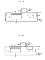
- FIG. 2 is a cross-sectional view illustrating an image sensor in accordance with a specific embodiment of the present invention.
- FIGS. 3A to 3D are cross-sectional views illustrating a method for fabricating an image sensor in accordance with the specific embodiment of the present invention.
- FIG. 2 is a cross-sectional view illustrating an image sensor in accordance with a specific embodiment of the present invention.
- Device isolation structure 304 is formed in a first conductivity type substrate 303 to define an active region and a device isolation region.
- the first conductivity type substrate 303 includes a P-type epitaxial layer 302 formed over a P + -type substrate 301 .
- a gate structure 307 is formed over the active region of the first conductivity type substrate 303 .
- the first conductivity type substrate 303 may include silicon.
- the gate structure 307 includes a gate conductive layer 306 formed over a gate insulation layer 305 .
- Spacers 309 are formed on both sidewalls of the gate structure 307 .
- an impurity region 308 doped with N-type impurities is formed in a predetermined portion of the first conductivity type substrate 303 where a photodiode is to be formed on one side of the gate structure 307 .
- a first epitaxial layer 311 doped with N-type impurities in-situ is formed over the impurity region 308 .
- a predetermined portion of the first conductivity type substrate 303 is etched to form a trench, and the first epitaxial layer 311 fills the trench thereafter.
- the first epitaxial layer 311 may include one of silicon (Si) and silicon germanium (SiGe). In order to improve charge transfer efficiency, a portion of the first epitaxial layer 311 can be formed to overlap with a bottom portion of the gate structure 307 . A depth of the trench ranges from approximately 1,800 ⁇ to approximately 2,200 ⁇ .
- a second epitaxial layer 312 doped with P-type impurities in-situ is formed over the first epitaxial layer 311 .
- the second epitaxial layer 312 is formed as a pinning layer including one of Si and SiGe, and a portion of the second epitaxial layer 312 contacts the first conductivity type substrate 303 .
- a thickness of the second epitaxial layer 312 ranges from approximately 20 ⁇ to approximately 1,000 ⁇ .
- a floating diffusion region 310 is formed on the other side of the gate structure 307 in the first conductivity type substrate 303 .
- FIGS. 3A to 3D are cross-sectional views illustrating a method for fabricating an image sensor in accordance with a specific embodiment of the present invention.
- a device isolation structure 204 is formed in a first conductivity type substrate 203 to define an active region and a device isolation region.
- the first conductivity type substrate 203 includes a P-type epitaxial layer 202 formed over a P + -type substrate 201 .
- the first conductivity type substrate 203 may include silicon.
- the lowly doped P-type epitaxial layer 202 formed over the highly doped P + -type substrate 201 is because the existence of the lowly doped P-type epitaxial layer 202 allows a larger and deeper increase of a depletion region of a photodiode. Thus, the ability of the photodiode for concentrating photocharges can be increased.
- Another reason is because having the highly doped P + -type substrate 201 below the P-type epitaxial layer 202 allows a fast reaggregation of photocharges before the photocharges diffuse into an adjacent unit pixel. Thus, random diffusion of the photocharges can be reduced, resulting in a reduced transfer function fluctuation of the photocharges.
- the device isolation structure 204 is formed by employing a shallow trench isolation (STI) process because the device isolation structure 204 generally does not have bird's beaks.
- STI shallow trench isolation
- the STI process is capable of reducing regions that electrically isolate devices.
- the gate structure 207 includes a gate insulation layer 205 and a gate conductive layer 206 .
- a second conductivity type impurity region 208 is formed by implanting N-type impurities into a predetermined region where the photodiode is to be formed, such that, the second conductivity type impurity region 208 is self-aligned with an edge of the gate structure 207 .
- Spacers 209 are formed on both sidewalls of the gate structure 207 .
- the spacers 209 are formed by: sequentially forming a buffer oxide layer and a nitride layer over the resultant structure obtained after forming the second conductivity type impurity region 208 ; and performing a dry etching process on the buffer oxide and nitride layers.
- a barrier layer is formed over the second conductivity type impurity region 208 and the gate structure 207 , and then, highly concentrated P-type impurities are implanted into a portion of the first conductivity type substrate 203 not covered by the barrier layer to form a floating diffusion region 210 . Then, the barrier layer is removed.
- a mask layer 211 is formed over the substrate structure obtained after the removal of the barrier layer.
- the mask layer 211 may include an oxide-based layer formed by employing a chemical vapor deposition (CVD) method.
- a predetermined portion of the mask layer 211 is removed.
- the predetermined portion corresponds to a portion formed over a region where the photodiode is to be formed.
- the first conductivity type substrate 203 is etched to form a trench using a patterned mask layer 211 A.
- the patterned mask layer 211 A is obtained by performing an etching process using hydrogen chloride (HCl). This etching process is performed at a temperature ranging from approximately 500° C. to approximately 5,000° C. with a pressure ranging from approximately 0.1 Torr to approximately 760 Torr.
- the second conductivity type impurity region 208 is formed below the trench.
- the trench has a thickness ranging from approximately 1,800 ⁇ to approximately 2,200 ⁇ .
- a first epitaxial layer 212 fills the trench.
- the first epitaxial layer 212 has a second conductivity type.
- the first epitaxial layer 212 includes one of Si and SiGe.
- the first epitaxial layer 212 is generally formed to overlap with a bottom portion of the gate structure 207 to increase the charge transfer efficiency.
- the first epitaxial layer 212 is doped with N-type impurities (i.e., the second conductivity type impurities) while growing, using a doping gas including phosphine (PH 3 ). Meanwhile, if SiGe is used as the first epitaxial layer 212 , a Ge source of germane (GeH 4 ) at a Ge concentration level of approximately 5% to approximately 100% is used.
- N-type impurities i.e., the second conductivity type impurities
- PH 3 phosphine
- a predetermined portion ‘A’ of the patterned mask layer 211 A is selectively etched to form a mask pattern 211 B.
- the mask pattern 211 B is used to form a second epitaxial layer having a larger width than the first epitaxial layer 212 .
- a second epitaxial layer 213 is grown over the first epitaxial layer 212 .
- the second epitaxial layer 213 has a first conductivity type.
- the second epitaxial layer 213 functions as a pinning layer, and includes one of Si and SiGe.
- the second epitaxial layer 213 is doped with P-type impurities (i.e., the first conductivity type impurities) in-situ while growing.
- the second epitaxial layer 213 is doped with the P-type impurities using a doping gas including diborane (B 2 H 6 ) at a concentration level ranging from approximately 1 ⁇ 10 17 cm ⁇ 3 to approximately 1 ⁇ 10 22 cm ⁇ 3 .
- a doping gas including diborane (B 2 H 6 ) at a concentration level ranging from approximately 1 ⁇ 10 17 cm ⁇ 3 to approximately 1 ⁇ 10 22 cm ⁇ 3 .
- the P-type impurity region having a small thickness with a uniform doping level can be formed by forming the second epitaxial layer with Si or SiGe doped in-situ, where the second epitaxial layer is the P-type impurity region formed over the photodiode including a P/N/P junction.
- Such P-type impurity region having the small thickness with the uniform doping level can secure carriers generated in the short wavelength region for the visible light (e.g. blue light), and thus, increases the sensor sensitivity.
- an improved photodiode having an improved light absorption per unit surface area when compared to the typical photodiode and high quantum efficiency for transferring the absorbed light into a photo-current can be formed by forming the first epitaxial layer with Si or SiGe doped in-situ, where the first epitaxial layer is part of the N-type impurity region in the P/N/P junction.
- a dangling bond generated by the ion implantation process can be prevented, and thus a noise can be removed by: forming the first epitaxial layer to partially contact the bottom portion of the gate electrode, improving the charge transfer efficiency; and doping the first and the second epitaxial layers in-situ while growing.
Landscapes
- Solid State Image Pick-Up Elements (AREA)
- Transforming Light Signals Into Electric Signals (AREA)
- Light Receiving Elements (AREA)
Priority Applications (1)
| Application Number | Priority Date | Filing Date | Title |
|---|---|---|---|
| US12/382,729 US7989245B2 (en) | 2005-07-11 | 2009-03-23 | Method for fabricating image sensor |
Applications Claiming Priority (2)
| Application Number | Priority Date | Filing Date | Title |
|---|---|---|---|
| KR2005-0062301 | 2005-07-11 | ||
| KR1020050062301A KR100657143B1 (ko) | 2005-07-11 | 2005-07-11 | 이미지 센서 및 그 제조 방법 |
Related Child Applications (2)
| Application Number | Title | Priority Date | Filing Date |
|---|---|---|---|
| US12/382,729 Division US7989245B2 (en) | 2005-07-11 | 2009-03-23 | Method for fabricating image sensor |
| US12/382,729 Continuation US7989245B2 (en) | 2005-07-11 | 2009-03-23 | Method for fabricating image sensor |
Publications (2)
| Publication Number | Publication Date |
|---|---|
| US20070007562A1 US20070007562A1 (en) | 2007-01-11 |
| US7508018B2 true US7508018B2 (en) | 2009-03-24 |
Family
ID=37617522
Family Applications (2)
| Application Number | Title | Priority Date | Filing Date |
|---|---|---|---|
| US11/482,770 Active 2027-01-01 US7508018B2 (en) | 2005-07-11 | 2006-07-10 | Image sensor having a highly doped and shallow pinning layer |
| US12/382,729 Active 2026-12-15 US7989245B2 (en) | 2005-07-11 | 2009-03-23 | Method for fabricating image sensor |
Family Applications After (1)
| Application Number | Title | Priority Date | Filing Date |
|---|---|---|---|
| US12/382,729 Active 2026-12-15 US7989245B2 (en) | 2005-07-11 | 2009-03-23 | Method for fabricating image sensor |
Country Status (3)
| Country | Link |
|---|---|
| US (2) | US7508018B2 (enExample) |
| JP (1) | JP2007027730A (enExample) |
| KR (1) | KR100657143B1 (enExample) |
Families Citing this family (14)
| Publication number | Priority date | Publication date | Assignee | Title |
|---|---|---|---|---|
| US7064406B2 (en) * | 2003-09-03 | 2006-06-20 | Micron Technology, Inc. | Supression of dark current in a photosensor for imaging |
| US7141836B1 (en) * | 2005-05-31 | 2006-11-28 | International Business Machines Corporation | Pixel sensor having doped isolation structure sidewall |
| US20080299700A1 (en) * | 2007-05-28 | 2008-12-04 | Bang-Chiang Lan | Method for fabricating photodiode |
| JP5400280B2 (ja) * | 2007-06-07 | 2014-01-29 | パナソニック株式会社 | 固体撮像装置 |
| US7875918B2 (en) * | 2009-04-24 | 2011-01-25 | Omnivision Technologies, Inc. | Multilayer image sensor pixel structure for reducing crosstalk |
| US20140312386A1 (en) * | 2009-09-02 | 2014-10-23 | Pixart Imaging Incorporation | Optoelectronic device having photodiodes for different wavelengths and process for making same |
| US8247854B2 (en) * | 2009-10-08 | 2012-08-21 | Electronics And Telecommunications Research Institute | CMOS image sensor |
| US20110169991A1 (en) * | 2010-01-08 | 2011-07-14 | Omnivision Technologies, Inc. | Image sensor with epitaxially self-aligned photo sensors |
| JP5870478B2 (ja) * | 2010-09-30 | 2016-03-01 | 富士通セミコンダクター株式会社 | 半導体装置の製造方法 |
| JP2012231026A (ja) | 2011-04-26 | 2012-11-22 | Toshiba Corp | 固体撮像装置 |
| FR3000605A1 (fr) * | 2012-12-31 | 2014-07-04 | St Microelectronics Crolles 2 | Photocapteur adapte a la mesure de temps de vol |
| CN104517976B (zh) * | 2013-09-30 | 2018-03-30 | 中芯国际集成电路制造(北京)有限公司 | Cmos图像传感器的像素结构及其形成方法 |
| CN114388536A (zh) * | 2020-10-21 | 2022-04-22 | 格科微电子(上海)有限公司 | 图像传感器形成方法及图像传感器 |
| US12349500B2 (en) * | 2022-12-06 | 2025-07-01 | Globalfoundries U.S. Inc. | Photodiode with insulator layer along intrinsic region sidewall |
Citations (4)
| Publication number | Priority date | Publication date | Assignee | Title |
|---|---|---|---|---|
| US5191399A (en) * | 1990-12-21 | 1993-03-02 | Mitsubishi Denki Kabushiki Kaisha | Solid-state imaging device with improved photodetector |
| KR20010093670A (ko) | 2000-03-28 | 2001-10-29 | 니시무로 타이죠 | 고체 촬상 장치 및 그 제조 방법 |
| KR20020030959A (ko) | 2000-10-19 | 2002-04-26 | 박종섭 | 포토다이오드 영역에 트렌치를 구비하는 이미지 센서 및그 제조 방법 |
| US20030173585A1 (en) * | 2002-03-12 | 2003-09-18 | Mitsubishi Denki Kabushiki Kaisha | Semiconductor device having solid-state image sensor with suppressed variation in impurity concentration distribution within semiconductor substrate, and method of manufacturing the same |
Family Cites Families (5)
| Publication number | Priority date | Publication date | Assignee | Title |
|---|---|---|---|---|
| JPS5812481A (ja) * | 1981-07-15 | 1983-01-24 | Toshiba Corp | 固体撮像素子 |
| JP2959460B2 (ja) * | 1996-01-30 | 1999-10-06 | 日本電気株式会社 | 固体撮像装置 |
| JP2751910B2 (ja) * | 1996-02-28 | 1998-05-18 | 日本電気株式会社 | 半導体受光素子及びその製造方法 |
| KR100406537B1 (ko) * | 2001-12-03 | 2003-11-20 | 주식회사 하이닉스반도체 | 반도체장치의 제조 방법 |
| JP4695824B2 (ja) * | 2003-03-07 | 2011-06-08 | 富士電機ホールディングス株式会社 | 半導体ウエハの製造方法 |
-
2005
- 2005-07-11 KR KR1020050062301A patent/KR100657143B1/ko not_active Expired - Lifetime
-
2006
- 2006-07-10 US US11/482,770 patent/US7508018B2/en active Active
- 2006-07-11 JP JP2006190892A patent/JP2007027730A/ja active Pending
-
2009
- 2009-03-23 US US12/382,729 patent/US7989245B2/en active Active
Patent Citations (4)
| Publication number | Priority date | Publication date | Assignee | Title |
|---|---|---|---|---|
| US5191399A (en) * | 1990-12-21 | 1993-03-02 | Mitsubishi Denki Kabushiki Kaisha | Solid-state imaging device with improved photodetector |
| KR20010093670A (ko) | 2000-03-28 | 2001-10-29 | 니시무로 타이죠 | 고체 촬상 장치 및 그 제조 방법 |
| KR20020030959A (ko) | 2000-10-19 | 2002-04-26 | 박종섭 | 포토다이오드 영역에 트렌치를 구비하는 이미지 센서 및그 제조 방법 |
| US20030173585A1 (en) * | 2002-03-12 | 2003-09-18 | Mitsubishi Denki Kabushiki Kaisha | Semiconductor device having solid-state image sensor with suppressed variation in impurity concentration distribution within semiconductor substrate, and method of manufacturing the same |
Also Published As
| Publication number | Publication date |
|---|---|
| KR100657143B1 (ko) | 2006-12-13 |
| US7989245B2 (en) | 2011-08-02 |
| US20090286345A1 (en) | 2009-11-19 |
| JP2007027730A (ja) | 2007-02-01 |
| US20070007562A1 (en) | 2007-01-11 |
Similar Documents
| Publication | Publication Date | Title |
|---|---|---|
| US7989245B2 (en) | Method for fabricating image sensor | |
| US8203174B2 (en) | Image sensor having an epitaxial layer doped in-situ | |
| KR100748342B1 (ko) | 씨모스 이미지 센서의 제조방법 | |
| JP5569153B2 (ja) | 固体撮像装置およびその製造方法 | |
| KR100882467B1 (ko) | 이미지센서 및 그 제조방법 | |
| US9123606B2 (en) | Pixel structures of CMOS imaging sensors | |
| US20050179072A1 (en) | Isolation region implant permitting improved photodiode structure | |
| US7323378B2 (en) | Method for fabricating CMOS image sensor | |
| KR100672729B1 (ko) | 씨모스 이미지 센서의 제조방법 | |
| US20090166687A1 (en) | Image Sensor and Method for Manufacturing the Same | |
| US7537971B2 (en) | Method for fabricating CMOS image sensor | |
| KR100882468B1 (ko) | 이미지센서 및 그 제조방법 | |
| US8089106B2 (en) | Image sensor and method for manufacturing the same | |
| KR100729742B1 (ko) | 이미지 센서의 제조방법 | |
| CN120730854B (zh) | 半导体结构及其制备方法、图像传感器 | |
| KR20110070075A (ko) | 이미지 센서 및 그 제조방법 | |
| KR20100050331A (ko) | 이미지 센서 및 그 제조 방법 | |
| KR101033397B1 (ko) | 이미지 센서의 제조 방법 | |
| KR20100138325A (ko) | 이미지 센서 및 그 제조 방법 | |
| KR20080014484A (ko) | 이미지 센서 및 그 형성 방법 | |
| KR20070049410A (ko) | 이미지 센서 및 그 제조방법 | |
| TW200847459A (en) | Method for fabricating photodiode |
Legal Events
| Date | Code | Title | Description |
|---|---|---|---|
| AS | Assignment |
Owner name: MAGNACHIP SEMICONDUCTOR, LTD., KOREA, REPUBLIC OF Free format text: ASSIGNMENT OF ASSIGNORS INTEREST;ASSIGNOR:CHA, HAN-SEOB;REEL/FRAME:018089/0352 Effective date: 20060705 |
|
| AS | Assignment |
Owner name: U.S. BANK NATIONAL ASSOCIATION, AS COLLATERAL TRUS Free format text: AFTER-ACQUIRED INTELLECTUAL PROPERTY KUN-PLEDGE AGREEMENT;ASSIGNOR:MAGNACHIP SEMICONDUCTOR, LTD.;REEL/FRAME:022277/0133 Effective date: 20090217 |
|
| STCF | Information on status: patent grant |
Free format text: PATENTED CASE |
|
| AS | Assignment |
Owner name: CROSSTEK CAPITAL, LLC, DELAWARE Free format text: ASSIGNMENT OF ASSIGNORS INTEREST;ASSIGNOR:MAGNACHIP SEMICONDUCTOR, LTD.;REEL/FRAME:022764/0270 Effective date: 20090514 Owner name: CROSSTEK CAPITAL, LLC,DELAWARE Free format text: ASSIGNMENT OF ASSIGNORS INTEREST;ASSIGNOR:MAGNACHIP SEMICONDUCTOR, LTD.;REEL/FRAME:022764/0270 Effective date: 20090514 |
|
| AS | Assignment |
Owner name: CROSSTEK CAPITAL, LLC, DELAWARE Free format text: CONFIRMATORY ASSIGNMENT;ASSIGNOR:MAGNACHIP SEMICONDUCTOR, LTD.;REEL/FRAME:022824/0935 Effective date: 20090612 |
|
| AS | Assignment |
Owner name: MAGNACHIP SEMICONDUCTOR, LTD., KOREA, REPUBLIC OF Free format text: PARTIAL RELEASE OF SECURITY INTEREST;ASSIGNOR:U.S. BANK NATIONAL ASSOCIATION, AS COLLATERAL TRUSTEE;REEL/FRAME:023075/0054 Effective date: 20090527 Owner name: MAGNACHIP SEMICONDUCTOR, LTD.,KOREA, REPUBLIC OF Free format text: PARTIAL RELEASE OF SECURITY INTEREST;ASSIGNOR:U.S. BANK NATIONAL ASSOCIATION, AS COLLATERAL TRUSTEE;REEL/FRAME:023075/0054 Effective date: 20090527 |
|
| AS | Assignment |
Owner name: INTELLECTUAL VENTURES II LLC, DELAWARE Free format text: MERGER;ASSIGNOR:CROSSTEK CAPITAL, LLC;REEL/FRAME:026637/0632 Effective date: 20110718 |
|
| FPAY | Fee payment |
Year of fee payment: 4 |
|
| FPAY | Fee payment |
Year of fee payment: 8 |
|
| MAFP | Maintenance fee payment |
Free format text: PAYMENT OF MAINTENANCE FEE, 12TH YEAR, LARGE ENTITY (ORIGINAL EVENT CODE: M1553); ENTITY STATUS OF PATENT OWNER: LARGE ENTITY Year of fee payment: 12 |