US7495307B2 - Columnar electric device - Google Patents
Columnar electric device Download PDFInfo
- Publication number
- US7495307B2 US7495307B2 US10/579,920 US57992004A US7495307B2 US 7495307 B2 US7495307 B2 US 7495307B2 US 57992004 A US57992004 A US 57992004A US 7495307 B2 US7495307 B2 US 7495307B2
- Authority
- US
- United States
- Prior art keywords
- electroconductive
- wire
- semiconductor
- columnar
- wires
- Prior art date
- Legal status (The legal status is an assumption and is not a legal conclusion. Google has not performed a legal analysis and makes no representation as to the accuracy of the status listed.)
- Expired - Fee Related
Links
Images


Classifications
-
- G—PHYSICS
- G01—MEASURING; TESTING
- G01J—MEASUREMENT OF INTENSITY, VELOCITY, SPECTRAL CONTENT, POLARISATION, PHASE OR PULSE CHARACTERISTICS OF INFRARED, VISIBLE OR ULTRAVIOLET LIGHT; COLORIMETRY; RADIATION PYROMETRY
- G01J5/00—Radiation pyrometry, e.g. infrared or optical thermometry
- G01J5/10—Radiation pyrometry, e.g. infrared or optical thermometry using electric radiation detectors
- G01J5/20—Radiation pyrometry, e.g. infrared or optical thermometry using electric radiation detectors using resistors, thermistors or semiconductors sensitive to radiation, e.g. photoconductive devices
-
- G—PHYSICS
- G01—MEASURING; TESTING
- G01D—MEASURING NOT SPECIALLY ADAPTED FOR A SPECIFIC VARIABLE; ARRANGEMENTS FOR MEASURING TWO OR MORE VARIABLES NOT COVERED IN A SINGLE OTHER SUBCLASS; TARIFF METERING APPARATUS; MEASURING OR TESTING NOT OTHERWISE PROVIDED FOR
- G01D5/00—Mechanical means for transferring the output of a sensing member; Means for converting the output of a sensing member to another variable where the form or nature of the sensing member does not constrain the means for converting; Transducers not specially adapted for a specific variable
- G01D5/26—Mechanical means for transferring the output of a sensing member; Means for converting the output of a sensing member to another variable where the form or nature of the sensing member does not constrain the means for converting; Transducers not specially adapted for a specific variable characterised by optical transfer means, i.e. using infrared, visible, or ultraviolet light
-
- G—PHYSICS
- G01—MEASURING; TESTING
- G01J—MEASUREMENT OF INTENSITY, VELOCITY, SPECTRAL CONTENT, POLARISATION, PHASE OR PULSE CHARACTERISTICS OF INFRARED, VISIBLE OR ULTRAVIOLET LIGHT; COLORIMETRY; RADIATION PYROMETRY
- G01J1/00—Photometry, e.g. photographic exposure meter
- G01J1/42—Photometry, e.g. photographic exposure meter using electric radiation detectors
-
- H—ELECTRICITY
- H10—SEMICONDUCTOR DEVICES; ELECTRIC SOLID-STATE DEVICES NOT OTHERWISE PROVIDED FOR
- H10D—INORGANIC ELECTRIC SEMICONDUCTOR DEVICES
- H10D62/00—Semiconductor bodies, or regions thereof, of devices having potential barriers
- H10D62/10—Shapes, relative sizes or dispositions of the regions of the semiconductor bodies; Shapes of the semiconductor bodies
-
- H—ELECTRICITY
- H10—SEMICONDUCTOR DEVICES; ELECTRIC SOLID-STATE DEVICES NOT OTHERWISE PROVIDED FOR
- H10K—ORGANIC ELECTRIC SOLID-STATE DEVICES
- H10K10/00—Organic devices specially adapted for rectifying, amplifying, oscillating or switching; Organic capacitors or resistors having potential barriers
- H10K10/40—Organic transistors
- H10K10/46—Field-effect transistors, e.g. organic thin-film transistors [OTFT]
- H10K10/462—Insulated gate field-effect transistors [IGFETs]
- H10K10/464—Lateral top-gate IGFETs comprising only a single gate
-
- H—ELECTRICITY
- H10—SEMICONDUCTOR DEVICES; ELECTRIC SOLID-STATE DEVICES NOT OTHERWISE PROVIDED FOR
- H10K—ORGANIC ELECTRIC SOLID-STATE DEVICES
- H10K10/00—Organic devices specially adapted for rectifying, amplifying, oscillating or switching; Organic capacitors or resistors having potential barriers
- H10K10/40—Organic transistors
- H10K10/46—Field-effect transistors, e.g. organic thin-film transistors [OTFT]
- H10K10/462—Insulated gate field-effect transistors [IGFETs]
- H10K10/466—Lateral bottom-gate IGFETs comprising only a single gate
-
- Y—GENERAL TAGGING OF NEW TECHNOLOGICAL DEVELOPMENTS; GENERAL TAGGING OF CROSS-SECTIONAL TECHNOLOGIES SPANNING OVER SEVERAL SECTIONS OF THE IPC; TECHNICAL SUBJECTS COVERED BY FORMER USPC CROSS-REFERENCE ART COLLECTIONS [XRACs] AND DIGESTS
- Y02—TECHNOLOGIES OR APPLICATIONS FOR MITIGATION OR ADAPTATION AGAINST CLIMATE CHANGE
- Y02E—REDUCTION OF GREENHOUSE GAS [GHG] EMISSIONS, RELATED TO ENERGY GENERATION, TRANSMISSION OR DISTRIBUTION
- Y02E10/00—Energy generation through renewable energy sources
- Y02E10/50—Photovoltaic [PV] energy
- Y02E10/549—Organic PV cells
-
- Y—GENERAL TAGGING OF NEW TECHNOLOGICAL DEVELOPMENTS; GENERAL TAGGING OF CROSS-SECTIONAL TECHNOLOGIES SPANNING OVER SEVERAL SECTIONS OF THE IPC; TECHNICAL SUBJECTS COVERED BY FORMER USPC CROSS-REFERENCE ART COLLECTIONS [XRACs] AND DIGESTS
- Y02—TECHNOLOGIES OR APPLICATIONS FOR MITIGATION OR ADAPTATION AGAINST CLIMATE CHANGE
- Y02P—CLIMATE CHANGE MITIGATION TECHNOLOGIES IN THE PRODUCTION OR PROCESSING OF GOODS
- Y02P70/00—Climate change mitigation technologies in the production process for final industrial or consumer products
- Y02P70/50—Manufacturing or production processes characterised by the final manufactured product
-
- Y—GENERAL TAGGING OF NEW TECHNOLOGICAL DEVELOPMENTS; GENERAL TAGGING OF CROSS-SECTIONAL TECHNOLOGIES SPANNING OVER SEVERAL SECTIONS OF THE IPC; TECHNICAL SUBJECTS COVERED BY FORMER USPC CROSS-REFERENCE ART COLLECTIONS [XRACs] AND DIGESTS
- Y10—TECHNICAL SUBJECTS COVERED BY FORMER USPC
- Y10T—TECHNICAL SUBJECTS COVERED BY FORMER US CLASSIFICATION
- Y10T29/00—Metal working
- Y10T29/49—Method of mechanical manufacture
- Y10T29/49002—Electrical device making
- Y10T29/49117—Conductor or circuit manufacturing
- Y10T29/49194—Assembling elongated conductors, e.g., splicing, etc.
Definitions
- the present invention relates to a columnar electric device including a sensor, solar cell, and the like, and a production method thereof. Particularly, the present invention relates to an electric device which can be downsized without degradation of a performance and can be mounted even in a narrow place, and a method for readily producing the electric device.
- an ammonia gas sensor including: an electrically insulative ceramic substrate; two comb-shaped electrodes formed thereon; and an ammonia sensitive layered film formed to extend over the two comb-shaped electrodes.
- a first embodiment of the invention resides in a production method of a columnar electric device, characterized in that the method comprises the steps of:
- a second embodiment resides in a production method of a columnar electric device, characterized in that the method comprises the steps of:
- a third embodiment resides in a production method of a columnar electric device, characterized in that the method comprises the steps of:
- a fourth embodiment resides in a production method of a columnar electric device, characterized in that the method comprises the step of:
- a fifth embodiment resides in a production method of a columnar electric device, characterized in that the method comprises the step of:
- a sixth embodiment resides in the production method of a columnar electric device of any one of the preceding first through fifth embodiments, characterized in that the columnar electric device is a sensor or solar cell.
- This electric device is produced by the method of any one of thge preceding first through fifth embodiments, for example,
- An eighth embodiment resides in the columnar electric device of the foregoing device, characterized in that the columnar body is a fibrous body.
- a ninth embodiment resides in a production method of a columnar electric device, characterized in that the method comprises the steps of:
- a tenth embodiment resides in a production method of a columnar electric device, characterized in that the method comprises the steps of:
- An eleventh embodiment resides in a production method of a columnar electric device, characterized in that the method comprises the steps of:
- a twelfth embodiment resides in a production method of a columnar electric device, characterized in that the method comprises the steps of:
- a thirteenth embodiment resides in a production method of a columnar electric device, characterized in that the method comprises the steps of:
- a fourteenth embodiment resides in a production method of a columnar electric device, characterized in that the method comprises the steps of:
- a fifteenth embodiment resides in the production method of a columnar electric device of any one of the foregoing ninth through fourteenth embodiments, characterized in that the columnar electric device is a sensor or solar cell.
- This electric device is produced by the method of any one of the preceding ninth through fourteenth embodiments, for example.
- a seventeenth embodiment resides in the columnar electric device of the fourteenth embodiment, characterized in that the columnar body is a fibrous body.
- This solar cell is produced by the method of any one of the ninth through fourteenth embodiments, for example.
- a nineteenth embodiment resides in the solar cell as described above, characterized in that the columnar body is a fibrous body.
- a twentieth embodiment resides in a production method of a columnar electric device, characterized in that the method comprises the steps of:
- a twenty-first embodiment resides in a production method of a columnar electric device, characterized in that the method comprises the steps of:
- a twenty-second embodiment resides in a production method of a columnar electric device, characterized in that the method comprises the steps of:
- a twenty-third embodiment resides in a production method of a columnar electric device, characterized in that the method comprises the steps of:
- a twenty-fourth embodiment resides in a production method of a columnar electric device, characterized in that the method comprises the step of:
- a twenty-fifth embodiment resides in a production method of a columnar electric device, characterized in that the method comprises the steps of:
- a twenty-sixth embodiment resides in the production method of a columnar electric device of any one of the five immediately foregoing methods, characterized in that the columnar electric device is a sensor or solar cell.
- a twenty-eighth embodiment resides in the columnar electric device of the twenty-seventh embodiment, characterized in that the columnar body is a fibrous body.
- This solar cell is produced by the method of any one of the twentieth through twenty-fifth embodiments, for example.
- a thirtieth embodiment resides in the solar cell of the twenty-ninth embodiment, characterized in that the columnar body is a fibrous body.
- a thirty-first embodiment resides in a production method of a columnar electric device, characterized in that the method comprises the steps of:
- a thirty-second embodiment resides in a production method of a columnar electric device, characterized in that the method comprises the steps of:
- a thirty-third embodiment resides in a production method of a columnar electric device, characterized in that the method comprises the steps of:
- a thirty-fourth embodiment resides in a production method of a columnar electric device, characterized in that the method comprises the steps of:
- a thirty-fifth embodiment resides in a production method of a columnar electric device, characterized in that the method comprises the steps of:
- a thirty-sixth embodiment resides in a production method of a columnar electric device, characterized in that the method comprises the steps of:
- a thirty-seventh embodiment resides in the production method of a columnar electric device of any one of the thirty-first through thirty-sixth embodiments, characterized in that the columnar electric device is a sensor or solar cell.
- a thirth-eighth embodiment resides in a columnar electric device, characterized in that the columnar electric device comprises:
- This electric device is produced by the method of any one of the thirty-first through thirty-sixth embodiments, for example.
- a thirth-ninth embodiment resides in the columnar electric device of the thirty-eighth embodiment, characterized in that the columnar body is a fibrous body.
- a fourtieth embodiment resides in a production method of a columnar electric device, characterized in that the method comprises the steps of:
- a fourty-first embodiment resides in a production method of a columnar electric device, characterized in that the method comprises the steps of:
- a fourty-second embodiment resides in the production method of a columnar electric device of the fourtieth or forty-first embodiment, characterized in that the columnar electric device is an optical sensor or solar cell.
- a forty-third embodiment resides in a columnar electric device, characterized in that the columnar electric device comprises:
- This electric device is produced by the method of any one of the fortiety through forty-second embodiments.
- a forty-fourth embodiment resides in a production method of a columnar transistor, characterized in that the method comprises the steps of:
- a forty-fifth embodiment resides in the production method of a columnar transistor of the forty-fourth embodiment, characterized in that the method further comprises the steps of:
- This columnar transistor is produced by the method of the forty-fourth or forty-fifth embodiment.
- the mask material such as a fabric, thread, or the like is helically wound onto the outer periphery of the columnar body, and thereafter the electroconductive wire is wound onto the outer periphery by coating the electroconductive substance onto the outer periphery through the helical gap defined by the mask material. It is desirable to adopt vapor deposition, application, or the like as coating, thereby enabling obtainment of a stable columnar electric device having the electroconductive wire closely contacted with the columnar body.
- the electroconductive wire it becomes possible to arrange the electroconductive wire while uniformalizing a diameter of the electroconductive wire and a helical gap defined thereby, to facilitate a task of designing and simulation. Further, winding a linear substance having a small diameter like a thread, enables production of a small-sized columnar electric device.
- the production method of the fifth embodiment is effective, when the electroconductive wire and the insulative wire exhibit a higher adhesiveness therebetween, for example, and readily follow a stress such as bending. It is desirable to use an epoxy adhesive for joining the electroconductive wire to the insulative wire and for joining them to the columnar body, and the columnar electric device can be produced by an extremely simple method.
- the columnar sensor or solar cell can be produced by the method of any one of the first through fifth embodiments.
- the seventh embodiment resides in the columnar electric device which can be downsized.
- Examples thereof include a temperature sensor, pressure sensor, ion sensor, and the like.
- the mentioned sensors adopt platinum, poly-3-alkylthiophene, and polyaniline, as the electroconductive wires, respectively.
- the columnar body can be downsized. It is desirable to adopt polyethylene terephthalate, polymethyl methacrylate, nylon, polyester, polypropylene, or the like, as the fibrous body. Simultaneously, according to the method of any one of the second through fifth embodiments, there can be obtained an extremely small-sized columnar electric device of 1 mm 3 or less, for example, by winding a thin electroconductive wire onto the columnar body with a fine interval to be defined by the electroconductive wire.
- the mask materials such as fabric, thread, or the like are helically wound onto the outside of the semiconductor coated on the columnar body, at first. Then, the electroconductive substances are coated onto the outside through the helical gaps defined by the mask materials, respectively, thereby winding the two electroconductive wires onto the outside. It is desirable to adopt vapor deposition, application, or the like as coating, thereby enabling obtainment of a stable columnar electric device having the two electroconductive wires closely contacted with the semiconductor.
- the electroconductive wires it becomes possible to arrange the electroconductive wires while uniformalizing diameters of the electroconductive wires and helical gaps defined thereby, to facilitate a task of designing and simulation. Further, winding linear substances having small diameters like threads, enables production of a small-sized columnar electric device. In case of using the same material for both the first electroconductive wire and second electroconductive wire, it is desirable to produce the electric device by the method recited in the twelfth embodiment.
- the production method of the thirteenth embodiment is effective, when the electroconductive wires and the insulative wires exhibit a higher adhesiveness therebetween, for example, and readily follow a stress such as bending. It is desirable to use an epoxy adhesive for joining the electroconductive wires to the insulative wires and for joining them to the columnar body, and the columnar electric device can be produced by an extremely simple method.
- the production method of the fourteenth embodiment is effective, when the first electroconductive wire and the insulative wires exhibit a higher adhesiveness therebetween, for example, and readily follow a stress such as bending. It is desirable to use an epoxy adhesive for joining the first electroconductive wire to the insulative wires and for joining them to the columnar body, and the columnar electric device can be produced by an extremely simple method.
- the columnar sensor or solar cell can be produced by the method of any one of the ninth through fourteenth embodiments.
- the sixteenth embodiment resides in a columnar electric device which can be downsized.
- Examples thereof include an optical sensor, gas sensor, humidity sensor, temperature sensor, radiation sensor, solar cell, and the like.
- the optical sensor is configured to use an organic semiconductor as the semiconductor, such as an electroconductive polymer, poly-p-phenylene, polythiophene, or the like doped with fullerene.
- the gas sensor is configured to use poly-p-phenylene, polyacetylene, polythiophene, or the like; the humidity sensor, polyfuran, polythiophene, or the like; the temperature sensor, poly-3-alkylthiophene, or the like; and the radiation sensor, polyacetylene, polythiophene, or the like in a sulfur hexafluoride atmosphere.
- the columnar optical sensor can be bent, it is also possible to immerse the portion of the optical sensor having the electroconductive wires wound thereon in a dopant solution, and to simultaneously apply a voltage to one of the electroconductive wires to thereby achieve doping.
- the eighteenth embodiment resides in a columnar solar cell produced by the method of any one of the ninth through fourteenth embodiments. It is possible to obtain a small-sized solar cell, by a simple production method.
- the columnar body can be downsized.
- the usable fibrous body is the same as that of embodiment 8 .
- Simultaneously, according to the method of any one of embodiments 10 through 14 there can be obtained an extremely small-sized columnar electric device, by winding thin electroconductive wires with fine intervals to be defined by the electroconductive wires.
- the twenty-first through twenty-third embodiments it becomes possible to arrange the electroconductive wires while uniformalizing diameters of the electroconductive wires and helical gaps defined thereby, to facilitate a task of designing and simulation. Further, winding linear substances having small diameters like threads, enables production of a small-sized columnar electric device. In case of using the same material for both the first electroconductive wire and second electroconductive wire, it is desirable to produce the electric device by the method recited in the twenty-third embodiment.
- the production method of the twenty-fourth embodiment is effective, when the electroconductive wires and the semiconductor wires exhibit a higher adhesiveness therebetween, for example, and readily follow a stress such as bending. It is desirable to use an epoxy adhesive for joining the electroconductive wires to the semiconductor wires and for joining them to the columnar body, and the columnar electric device can be produced by an extremely simple method.
- the production method of the twenty-fifth embodiment is effective, when the first electroconductive wire and the semiconductor wires exhibit a higher adhesiveness therebetween, for example, and readily follow a stress such as bending. It is desirable to use an epoxy adhesive for joining the first electroconductive wire to the semiconductor wires and for joining them to the columnar body, and the columnar electric device can be produced by an extremely simple method.
- the columnar sensor or solar cell can be produced by the method of any one of the twentieth through twenty-fifth embodiment.
- the twenty-seventh embodiment resides in a columnar electric device which can be downsized. The contents thereof are the same as the sixteenth embodiment.
- the twenty-ninth embodiment resides in a solar cell produced by the method of any one of the twentiety through twenty-fifth embodiments. It is possible to obtain a small-sized solar cell, by a simple production method.
- the columnar body can be downsized.
- the usable fibrous body is the same as that of the eighth embodiment.
- the mask materials such as fabric, thread, or the like are helically wound onto the outside of the first semiconductor coated on the columnar body, at first.
- the electroconductive substances are coated onto the outside through the helical gaps defined by the mask materials, respectively, thereby winding the two electroconductive wires onto the outside.
- the second semiconductor is coated onto the outside through each helical gap defined by the two electroconductive wires therebetween. It is desirable to adopt vapor deposition, application, or the like as coating, thereby enabling obtainment of a stable columnar electric device having the two electroconductive wires and the second semiconductor closely contacted with the first semiconductor.
- the thirty-second through thirty-fourth embodiments it becomes possible to arrange the electroconductive wires while uniformalizing diameters of the electroconductive wires and helical gaps defined thereby, to facilitate a task of designing and simulation. Further, winding linear substances having small diameters like threads, enables production of a small-sized columnar electric device. In case of using the same material for both the first electroconductive wire and second electroconductive wire, it is desirable to produce the electric device by the method recited in the thirty-fourth embodiment.
- the production method of the thirty-fifth embodiment is effective, when the electroconductive wires and the semiconductor wires exhibit a higher adhesiveness therebetween, for example, and readily follow a stress such as bending. It is desirable to use an epoxy adhesive for joining the electroconductive wires to the insulative wires and for joining them to the columnar body, and the columnar electric device can be produced by an extremely simple method.
- the production method of the thirty-sixth embodiment is effective, when the first electroconductive wire and the semiconductor wires exhibit a higher adhesiveness therebetween, for example, and readily follow a stress such as bending. It is desirable to use an epoxy adhesive for joining the first electroconductive wire to the semiconductor wires and for joining them to the columnar body, and the columnar electric device can be produced by an extremely simple method.
- the columnar sensor or solar cell can be produced by the method of any one of the thirty-first through thirty-sixth embodiments.
- the thirty-eighth embodiment resides in a columnar electric device which can be downsized. The contents thereof are the same as the sixteenth embodiment.
- the columnar body can be downsized.
- the usable fibrous body is the same as that of the eighth embodiment, Simultaneously, according to the method of the thirty-first through thirty-sixth embodiments, for example, there can be obtained an extremely small-sized columnar electric device, by winding thin electroconductive wires and/or semiconductor wires with fine intervals to be defined by the electroconductive wires and/or semiconductor wires, respectively.
- the semiconductor is coated onto the outer periphery of the electroconductive columnar body, and then the electroconductive wire is wound onto the outside of the semiconductor. It is desirable to adopt vapor deposition, application, or the like as coating. It is desirable to adopt the method of any one of the first through fifth embodiments, for example, and the electroconductive columnar body and the electroconductive wire are closely contacted with each other through the semiconductor. This allows for production of a columnar electric device which operates stably.
- the semiconductor is coated onto the outer periphery of the electroconductive columnar body, the transparent electrode is subsequently coated onto the outside of the semiconductor, and the electroconductive wire is further wound onto the outside of the transparent electrode. It is desirable to adopt vapor deposition, application, or the like as coating. It is desirable to adopt the method of any one of the first through fifth embodiments, for example, and the electroconductive columnar body and the electroconductive wire are closely contacted with each other through the semiconductor and the transparent electrode. Namely, even when the transparent electrode is partially cracked due to stress such as bending, the electroconductive wire fixes the transparent electrode while electrically contacting with the same. This allows for production of a columnar electric device which operates stably.
- a columnar optical sensor or solar cell which has an electroconductive columnar body, a semiconductor, and a transparent electrode, and which operates stably.
- the forty-third embodiment resides in a columnar electric device which can be downsized.
- the insulating material is coated onto the outer periphery of the electroconductive columnar body, and the two electroconductive wires are subsequently wound onto the outside of the insulating material. It is desirable to adopt vapor deposition, application, or the like as coating. It is desirable to adopt the method of any one of the ninth through fourteenth embodiments, and the electroconductive columnar body and the two electroconductive wires are closely contacted with each other through the insulating material. This allows for obtainment of a columnar electric device which operates stably.
- the forty-fifth embodiment it becomes possible to readily produce a transistor having the doped insulating material.
- the columnar transistor produced by the method of the forty-fourth embodiment can be bent, the columnar transistor is bent and immersed into the dopant solution such that the portion of the transistor having the electroconductive wires wound thereon is immersed in the dopant solution. Further, there is applied a voltage to the electroconductive columnar body, for example, thereby achieving doping. It is also possible to observe a state of the doping, by causing electric current to flow between the two electroconductive wires. Namely, it is possible to perform the doping at an appropriate amount for the insulating material, while confirming the state of the doping.
- the forty-sixth embodiment resides in a columnar transistor which can be downsized.
- FIG. 1 A perspective view of a temperature sensor as one type of “columnar electric device comprising a single wire” according to the present invention.
- FIG. 2 A schematic view of a typical production method of the “columnar electric device comprising a single wire”.
- FIG. 3 A schematic view of an example of a production method of a “columnar electric device comprising a single wire” having a uniformly wound electroconductive wire.
- FIG. 4 A schematic view of another example of a production method of a “columnar electric device comprising a single wire” having a uniformly wound electroconductive wire.
- FIG. 5 A perspective view of an optical sensor as one type of “columnar electric device comprising a plate-like semiconductor” according to the present invention.
- FIG. 6 A schematic view of an example of a production method of a “columnar electric device comprising a plate-like semiconductor” having uniformly wound electroconductive wires.
- FIG. 7 A schematic view of another example of a production method of a “columnar electric device comprising a plate-like semiconductor” having uniformly wound electroconductive wires.
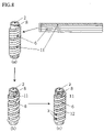
- FIG. 8 A schematic view of still another example of a production method of a “columnar electric device comprising a plate-like semiconductor” having uniformly wound electroconductive wires.
- FIG. 9 A perspective view of a “columnar electric device comprising a semiconductor wire” according to the present invention.
- FIG. 10 A perspective view of a “columnar electric device using two kinds of semiconductors” according to the present invention.
- FIG. 11 A perspective view of an example of a production method of a small-sized temperature sensor.
- FIG. 12 A perspective view of an optical sensor as an embodiment of a “columnar electric device having an electroconductive columnar body” according to the present invention.
- FIG. 13 A perspective view of an optical sensor as another embodiment of a “columnar electric device having an electroconductive columnar body” according to the present invention.
- FIG. 14 A schematic view of a doping method of a columnar transistor.
- Columnar electric device is an electric device in a columnar shape such as a circular column, polygonal column, or the like. Examples thereof include a columnar sensor, solar cell, and the like.
- “Columnar body” is a substrate having an outer periphery around which electroconductive wire(s), semiconductor wire(s), or the like is/are wound to fabricate a columnar electric device such as a sensor, solar cell, or the like.
- the present invention utilizes both electroconductive and insulative ones.
- insulative materials include plastics, quartz, sapphire, and the like.
- Coating is to coat an electroconductive wire, semiconductor wire, or the like around an outer periphery of a columnar body. As an example, coating is performed by vapor deposition of a substance to be coated, or application of a substance to be coated in a melt, solution, or gel state.
- “Mask material” is provided to cover a part of a side surface of a columnar body when an electroconductive wire(s), semiconductor wire(s), or the like is/are coated onto an outer periphery of the columnar body such that an unintended zone of the columnar body is not coated.
- FIG. 1 is a perspective view of a temperature sensor as one type of “columnar electric device comprising a single wire” according to the present invention.
- the platinum wire 4 has opposite sides having taps 3 mounted thereon, respectively, which are connected to a measuring instrument 1 to measure a resistance value to enable recognition of temperature.
- FIG. 2 shows a method for fabricating a temperature sensor by a vapor deposition method.
- a there is helically wound a coating-oriented mask material 5 around an outer periphery of an insulative columnar body 2 , and fixed thereto.
- platinum is coated onto the outer periphery such as by vapor deposition through a helical gap defined by the fabric 5 , thereby forming a platinum wire 4 .
- the mask material 5 is removed as shown in (c).
- taps 3 are mounted to opposite sides of the platinum wire 4 , respectively, for completion.
- FIG. 3 shows another method for uniformly winding a platinum wire by a vapor deposition method.
- a plate-like product provided by mutually joining two insulative wires 6 into a stripe shape. This is wound onto an outer periphery of an insulative columnar body 2 , and fixed thereto by an adhesive or the like as shown in (a).
- one of the insulative wires 6 is peeled off, as shown in (b). For example, it is sufficient to pinch one end of the applicable insulative wire 6 by hand, tweezers or the like, and to peel it along an outer periphery of the columnar body 2 .
- platinum is vapor deposited onto the outer periphery through the trace as shown in (c), thereby forming a platinum wire 4 .
- taps 3 are mounted to opposite sides of the platinum wire 4 , respectively, for completion.
- the insulative wires 6 for constituting the plate-like product are not limited to two in number.
- the plate-like product by a linear substance other than the insulative wire 6 .
- the linear substance left on the outer periphery of the columnar body 2 is to be peeled off after finishing vapor deposition of platinum in (c).
- Adoption of the vapor deposition method shown in FIG. 3 enables the platinum wire 4 to be adjusted in diameter and in helical gap, and to be uniformly wound. Further, adoption of a linear substance such as a thread enables the platinum wire 4 to be thin in diameter and to define a narrower helical gap. This allows for fabrication of a small-sized temperature sensor.
- an insulative wire 6 it is possible to wind an electroconductive wire such as a plate-like product obtained by mutually joining platinum wires into a stripe shape, onto an outer periphery of a columnar body 2 .
- the plate-like product comprising a plurality of platinum wires is densely wound onto an outer periphery of the columnar body 2 , and fixed thereto by a two-part epoxy adhesive, for example.
- a ceramic adhesive such as Sauereisen Cement of Nilaco Corporation.
- the fixing of the plate-like product comprising the plurality of platinum wires onto the outer periphery of the columnar body 2 may be performed by heating at 130° C., for example.
- FIG. 11 is a perspective view showing an example of a production method of the temperature sensor. This was provided by densely winding two platinum wires 4 each having a diameter of 0.02 mm onto a part of a columnar body made of a fibrous body, and by peeling off one of the platinum wires.
- the resultant product is to be exemplarily placed on a table 15 to cut opposite ends of the columnar body having the platinum wire wound thereon, thereby producing an extremely small-sized sensor. Adopting this temperature sensor allows for the same to be set in a narrow space to measure a temperature there.
- electroconductive wires to be wound on the outer periphery of the columnar body 2 include those other than metal, such as organic electroconductive wires, for example.
- coating may be performed by application of an organic electric conductor in a melt, solution, or gel state, instead of vapor deposition at (c).
- a pressure sensor adopting poly-3-alkylthiophene as an organic electric conductor an ion sensor adopting ponyaniline, and the like. It is desirable to apply an organic electric conductor dissolved in a coating-material aimed solvent, such as a toluene or xylene solution, onto the outer periphery of the columnar body 2 . Only, it is required to adopt a columnar body 2 and a mask material, which are insoluble in the coating-material aimed solvent.
- the former pressure sensor is largely changed in electrical conductivity by a change of pressure, even at a lower pressure.
- the latter ion sensor is configured to detect a pH value of an aqueous solution, by measuring a voldammogram of ponyaniline immersed in the aqueous solution.
- the plate-like product obtained by mutually bonding them is capable of readily following a bending stress.
- the plate-like product obtained by mutually joining an insulative wire 6 and an electroconductive wire 7 into a stripe shape is wound onto an outer periphery of a columnar body 2 , and is fixed thereto by an adhesive or the like.
- FIG. 5 is a perspective view of an optical sensor as one type of “columnar electric device comprising a plate-like semiconductor” according to the present invention.
- a semiconductor 8 Coated in a plate shape around an outer periphery of an insulative columnar body 2 , is a semiconductor 8 , such as an organic semiconductor comprising electroconductive polymer doped with fullerene, for example. Additionally wound onto an outside thereof are a copper wire 9 and an aluminum wire 10 . Light irradiated to the sensor is converted into electricity by the semiconductor 8 . It is possible to know an intensity of light irradiated to the sensor, by measuring an electric current flowing between the copper wire 9 and aluminum wire 10 by a measuring instrument 1 .
- the electroconductive polymer it is possible to adopt poly-3-alkylthiophene, poly-2,5-dioxythyroxy-p-phenylenevinylene, and the like.
- poly-3-hexylthiophene as one kind of poly-3-alkylthiophene, it is desirable to previously dope 20 to 30 wt % of fullerene.
- the columnar optical sensor When the columnar optical sensor can be bent, it is also possible to immerse the portion having the electroconductive wires wound thereon in a dopant solution, and to simultaneously apply a voltage to one of the electroconductive wires to thereby achieve doping. Namely, it is also possible to perform suitable doping by a simple method.
- Coating of an outer periphery of a columnar body 2 by a semiconductor 8 is achieved by vapor depositing the semiconductor 8 thereto.
- coating is performed by application of the semiconductor 8 in a melt, solution, or gel state, onto the columnar body 2 .
- a semiconductor dissolved in a coating-material aimed solvent such as a toluene or xylene solution, onto the outer periphery of the columnar body 2 . Only, it is required to adopt a columnar body 2 which is insoluble in the coating-material aimed solvent.
- the winding of the copper wire 9 and aluminum wire 10 onto an outside of the columnar body can be achieved by the same method as that explained in FIG. 2 .
- the mask material for coating such as a fabric 5 , is helically wound and fixed thereto.
- copper is coated such as by vapor deposition, to form a copper wire 9 through a helical gap defined by the fabric 5 .
- the fabric 5 wound for formation of the copper wire 9 is removed, and then another fabric 5 is helically wound to cover the copper wire 9 and is fixed.
- This is followed by vapor deposition of aluminum, to form an aluminum wire 10 through a helical gap defined by the fabric 5 .
- the fabric 5 wound for formation of the aluminum wire 10 is removed, and then taps 3 are finally mounted to the copper wire 9 and aluminum wire 10 , respectively, for completion.
- FIG. 6 In uniformly winding the copper wire 9 and aluminum wire 10 , it is desirable to adopt a method shown in FIG. 6 .
- a a plate-like product obtained by mutually joining four insulative wires 6 into a stripe shape, for example.
- the plate-like product After coating a semiconductor 8 onto an outer periphery of a columnar body 2 , the plate-like product is wound onto an outside of the semiconductor and fixed thereto.
- one of the four insulative wires 6 is peeled off, and copper is vapor deposited onto the outside through a trace of the peeled insulative wire to thereby form a copper wire 9 .
- one of the insulative wires 6 which is not neighboring to the vapor deposited copper wire 9 , is peeled off, and aluminum is vapor deposited onto the outside through a trace of the peeled insulative wire to thereby form an aluminum wire 10 .
- taps 3 are mounted to the copper wire 9 and aluminum wire 10 , respectively, for completion.
- the insulative wires 6 constituting the plate-like product is not limited to four in number. It is also possible to wind a plate-like product obtained by mutually joining four or more insulative wires 6 into a stripe shape, onto a columnar body 2 . Thereafter, one or more of the insulative wires 6 is/are peeled off, and copper at a trace(s) of the peeled wire(s) is vapor deposited onto the outer periphery of the columnar body to form a copper wire 9 .
- one or more of the insulative wires 6 which is/are not neighboring to the copper wire 9 , is/are peeled off, and aluminum is vapor deposited onto the outer periphery through a trace(s) of the peeled wire(s) to form an aluminum wire 10 .
- This is also applicable to a “columnar electric device comprising a semiconductor wire” and a “columnar electric device using two kinds of semiconductors”.
- the plate-like product by linear substances other than the insulative wires 6 .
- the linear substance left on the outer periphery of the semiconductor 8 is to be peeled off after omitting vapor deposition of platinum in (e).
- Adoption of the vapor deposition method shown in FIG. 6 enables the copper wire 9 and aluminum wire 10 to be each adjusted in diameter and in helical gap, and to be uniformly wound. Further, adoption of threads as the insulative wires 6 enables the copper wire 9 and aluminum wire 10 to be each thin in diameter and to define a narrower helical gap. This allows for fabrication of a small-sized optical sensor.
- Examples of the two electroconductive wires to be wound on the outside of the columnar body 2 coated with the semiconductor 8 include those other than metal, such as organic electroconductive wires.
- coating may be performed by application of an organic electric conductor in a melt, solution, or gel state, instead of vapor deposition at (c) and (e).
- FIG. 8 shows another fabrication method. This is to fabricate one of two electroconductive wires by winding, and the other by vapor deposition. Firstly, as shown in (a), there is prepared a plate-like product obtained by mutually joining one first electroconductive wire 11 and three insulative wires 6 into a stripe shape. After coating a semiconductor 8 onto an outer periphery of a columnar body 2 , the plate-like product is wound onto an outside of the semiconductor and fixed thereto.
- Examples of a “columnar electric device comprising a plate-like semiconductor and two electroconductive wires” to which the present invention is applicable, include the following sensors, in addition to the above optical sensor.
- gas sensors utilizing poly-p-phenylene, polyacetylene, polythiophene, or the like, as a semiconductor 8 . These semiconductors are each changed in electrical conductivity, by contact with nitrogen monoxide (NO) gas, ammonia (NH 3 ) gas, or the like. The gas concentration is measured by a change of electrical conductivity.
- NO nitrogen monoxide
- NH 3 ammonia
- sensors utilizing polyfuran, polythiophene, or the like as a semiconductor 8 . There is measured a humidity, by a change of electrical conductivity in case of polyfuran, and by a change of electric potential between two electroconductive wires contacted with the semiconductor made of polythiophene.
- optical sensors utilizing poly-p-phenylene, polythiophene, and the like as a semiconductor 8 .
- the poly-p-phenylene is to utilize a light induced isomerization reaction (transformation between quinoid structure and benzenoid structure due to light).
- Polythiophene causes light induced doping, by making the same to carry a substance such as photodissociative triphenyl iodonium tetrafluoroborate or the like.
- Polythiophene is capable of constituting a sensor utilizing such light induced doping.
- an extremely small-sized columnar electric device also by the “columnar electric device comprising a plate-like semiconductor”.
- a fibrous body such as polyethylene terephthalate or the like, as a columnar body 2 .
- a semiconductor 8 comprising organic compound at a thickness of 50 to 500 ⁇ m.
- an electroconductive wire of 0.05 to 1 mm in diameter, thereby enabling obtainment of an extremely small-sized columnar electric device.
- FIG. 9 is a perspective view of an “organic electric device comprising a semiconductor wire” according to the present invention. This is provided by winding a first electroconductive wire 11 and a second electroconductive wire 12 around an insulative columnar body 2 , and by coating semiconductors 8 between the two electroconductive wires, respectively.
- the two electroconductive wires are wound in the same manner as the above described columnar electric device. Thereafter, it is desirable to peel off the remaining linear substances, and to coat the semiconductors 8 onto the outer periphery through the traces of the peeled substances. It is also possible to perform the coating of the semiconductors 8 , by various methods including vapor deposition, or application of a semiconductor in a melt, solution, or gel state.
- a plate-like product to be obtained by mutually joining four wires in an order of a semiconductor wire, a first electroconductive wire, a semiconductor wire, and a second electroconductive wire into a stripe shape. This is wound onto an outer periphery of a columnar body and fixed thereto, followed by mounting of taps to the first electroconductive wire and second electroconductive wire, respectively, for completion.
- a plate-like product obtained by mutually joining a first electroconductive wire and three semiconductor wires into a stripe shape This plate-like product is wound onto an outer periphery of a columnar body, and fixed thereto. Thereafter, there is peeled off the semiconductor wire which is not neighboring to the first electroconductive wire, and there is coated a second electroconductive substance onto the outer periphery through the trace to thereby form a second electroconductive wire. Finally, taps are mounted to the first electroconductive wire and second electroconductive wire, respectively, for completion.
- FIG. 10 is a perspective view of a “columnar electric device using two kinds of semiconductors” according to the present invention.
- a first semiconductor 13 onto an outer periphery of an insulative columnar body 2
- a first electroconductive wire 11 and a second electroconductive wire 12 onto an outside of the first semiconductor.
- second semiconductors 14 between the two electroconductive wires.
- the usage of sensors according to the present invention can be increased, such as an increased number of kinds of detectable gases.
- FIG. 12 is a perspective view of an optical sensor as an embodiment of a “columnar electric device having an electroconductive columnar body” according to the present invention.
- Coated on an outer periphery of an electroconductive columnar body 16 is a semiconductor 17 .
- Wound around an outside thereof is an electroconductive wire 19 .
- the electroconductive columnar body 16 is made of aluminum, for example.
- the semiconductor 17 is coated onto an outer periphery of the electroconductive columnar body 16 .
- the semiconductor 17 is made of an electroconductive polymer doped with fullerene, for example.
- the electroconductive polymer it is possible to adopt poly-3-alkylthiophene, poly-2,5-dioxythyroxy-p-phenylenevinylene, and the like. In case of adoption of poly-3-hexylthiophene as one kind of poly-3-alkylthiophene, it is desirable to previously dope 20 to 30 wt % of fullerene.
- the coating of the semiconductor 17 is performed by vapor deposition, or application of a semiconductor in a melt, solution, or gel state.
- an electroconductive wire 19 such as a copper wire, onto an outside of the semiconductor 17 . It is desirable to perform the winding of the electroconductive wire 19 in the same manner as the winding of the platinum wire explained in the “columnar electric device comprising a single wire”. After winding the electroconductive wire 19 , a tap 3 is mounted to the electroconductive wire 19 for completion.
- the electroconductive columnar body 16 made of aluminum is different from the electroconductive wire 19 made of a copper wire in work function, so that there is generated an electric potential difference between the columnar body 16 and electroconductive wire 19 upon irradiation of light to the semiconductor 17 .
- Measuring the electric potential difference by a measuring instrument allows for measurement of an intensity of light irradiated to the semiconductor 17 through a helical gap defined by the electroconductive wire 19 , for example.
- the optical sensor shown in FIG. 12 can also be utilized as a solar cell. Further, adoption of a gold wire instead of the copper wire as the electroconductive body wire 19 enables an efficiency of photoelectric conversion to be improved.
- the semiconductor 17 it is desirable to adopt an organic compound such as the above described electroconductive polymer and the like, in a manner to coat it onto an outer periphery of the electroconductive columnar body 16 at a thickness of 50 to 500 ⁇ m. Further, as explained in FIG. 11 , winding a copper wire which is thin in diameter, allows for obtainment of an extremely small-sized optical sensor or solar cell.
- FIG. 13 is a perspective view of an optical sensor as another embodiment of a “columnar electric device having an electroconductive columnar body” according to the present invention, and the same elements as those in FIG. 12 are denoted by the same reference numerals, respectively.
- It includes a transparent electrode 18 coated on an outside of a semiconductor 17 .
- the optical sensor is configured with an electroconductive columnar body 16 , the semiconductor 17 , and the transparent electrode 18 . Namely, there is generated an electric potential difference between the columnar body 16 and the transparent electrode 18 commensurately with an intensity of light directly irradiated to an exposed portion of the semiconductor 17 and irradiated thereto through the transparent electrode 18 , and there is caused an electric current to flow between the columnar body and transparent electrode by connection thereof.
- the transparent electrode 18 is brittle, and tends to be broken due to cracks upon bending the same.
- there is additionally wound an electroconductive wire 19 onto an outside of the transparent electrode 18 to fix the transparent electrode 18 while electrically contacting with the same, in the present invention.
- the transparent electrode 18 is coated by vapor deposition, or application of a transparent electrode material in a melt, solution, or gel state.
- a transparent electrode material indium-tin-oxide (ITO), polyvinyl alcohol (PVA), and the like, for example.
- ITO indium-tin-oxide
- PVA polyvinyl alcohol
- the electroconductive wire 19 such as a copper wire is additionally wound onto an outside of the transparent electrode 18 .
- the winding of the electroconductive wire 19 is desirably performed in the same manner as the winding of a platinum wire explained in the “columnar electric device comprising a single wire”. After winding the electroconductive wire 19 , a tap 3 is mounted to the electroconductive wire 19 for completion.
- Irradiation of light to the semiconductor 17 generates an electric potential difference between the columnar body 16 and transparent electrode 18 , since the columnar body 16 made of aluminum and the transparent electrode 18 are different from each other in work function. It is possible to know an intensity of light irradiated to the semiconductor 17 , by measuring the electric potential difference by a measuring instrument 1 .
- the optical sensor shown in FIG. 13 can also be utilized as a solar cell.
- a columnar transistor for example, there is coated an insulating material onto an insulative columnar body.
- the coating is performed by vapor deposition, or application of an insulating material in a melt, solution, or gel state.
- Two electroconductive wires are wound around an outside thereof, for completion. For winding the two electroconductive wires, it is desirable to adopt the method recited in any one of the ninth through fourteenth embodiments.
- FIG. 14 is a schematic view thereof.
- Immersed into a dopant solution 23 is a columnar transistor obtained by coating an insulating material 21 onto an electroconductive columnar body (gate electrode) 20 and by winding two electroconductive wires (source electrode and drain electrode) 22 therearound, such that the portion of the insulating material having the electroconductive wires wound thereon is immersed in the dopant solution. Further, there is applied a voltage to the gate electrode, thereby achieving doping of the coated insulating material 21 . It is also possible to observe a state of the doping, by causing electric current to flow between the two electroconductive wires. Namely, it is possible to perform the doping at an appropriate amount for the insulating material 21 , while confirming the state of the doping.
- insulative columnar bodies 2 and electroconductive columnar bodies 16 have been each expressed by a circular shape in longitudinal cross-section, these are not limited thereto. For example, rectangular shapes, polygonal shapes, and other shapes will do.
- the columnar electric devices according to the present invention can be extremely downsized.
- the devices can be utilized as sensors and the like which are installed in narrow spaces such as gaps of machines, so as to measure a local temperature, gas concentration, and the like.
Landscapes
- Physics & Mathematics (AREA)
- General Physics & Mathematics (AREA)
- Spectroscopy & Molecular Physics (AREA)
- Photovoltaic Devices (AREA)
- Light Receiving Elements (AREA)
- Electroluminescent Light Sources (AREA)
- Thin Film Transistor (AREA)
- Investigating Or Analyzing Materials By The Use Of Electric Means (AREA)
- Investigating Or Analyzing Materials By The Use Of Fluid Adsorption Or Reactions (AREA)
- Measuring Temperature Or Quantity Of Heat (AREA)
Applications Claiming Priority (3)
| Application Number | Priority Date | Filing Date | Title |
|---|---|---|---|
| JP2003390149 | 2003-11-20 | ||
| JP2003-390149 | 2003-11-20 | ||
| PCT/JP2004/017367 WO2005050745A1 (ja) | 2003-11-20 | 2004-11-22 | 柱状電気素子及びその製造方法 |
Related Parent Applications (1)
| Application Number | Title | Priority Date | Filing Date |
|---|---|---|---|
| PCT/JP2004/017367 A-371-Of-International WO2005050745A1 (ja) | 2003-11-20 | 2004-11-22 | 柱状電気素子及びその製造方法 |
Related Child Applications (1)
| Application Number | Title | Priority Date | Filing Date |
|---|---|---|---|
| US12/208,567 Division US7763912B2 (en) | 2003-11-20 | 2008-09-11 | Columnar electric device and production method thereof |
Publications (2)
| Publication Number | Publication Date |
|---|---|
| US20070108556A1 US20070108556A1 (en) | 2007-05-17 |
| US7495307B2 true US7495307B2 (en) | 2009-02-24 |
Family
ID=34616328
Family Applications (2)
| Application Number | Title | Priority Date | Filing Date |
|---|---|---|---|
| US10/579,920 Expired - Fee Related US7495307B2 (en) | 2003-11-20 | 2004-11-22 | Columnar electric device |
| US12/208,567 Expired - Fee Related US7763912B2 (en) | 2003-11-20 | 2008-09-11 | Columnar electric device and production method thereof |
Family Applications After (1)
| Application Number | Title | Priority Date | Filing Date |
|---|---|---|---|
| US12/208,567 Expired - Fee Related US7763912B2 (en) | 2003-11-20 | 2008-09-11 | Columnar electric device and production method thereof |
Country Status (3)
| Country | Link |
|---|---|
| US (2) | US7495307B2 (enExample) |
| JP (6) | JPWO2005050745A1 (enExample) |
| WO (1) | WO2005050745A1 (enExample) |
Cited By (1)
| Publication number | Priority date | Publication date | Assignee | Title |
|---|---|---|---|---|
| US20090008635A1 (en) * | 2003-11-20 | 2009-01-08 | Ideal Star Inc. | Columnar electric device and production method thereof |
Families Citing this family (13)
| Publication number | Priority date | Publication date | Assignee | Title |
|---|---|---|---|---|
| JP5098197B2 (ja) * | 2006-03-27 | 2012-12-12 | 株式会社デンソー | 蓄電素子モジュール |
| US20070254593A1 (en) * | 2006-04-28 | 2007-11-01 | Medtronic Minimed, Inc. | Wireless data communication for a medical device network that supports a plurality of data communication modes |
| US8073008B2 (en) * | 2006-04-28 | 2011-12-06 | Medtronic Minimed, Inc. | Subnetwork synchronization and variable transmit synchronization techniques for a wireless medical device network |
| US20070255126A1 (en) * | 2006-04-28 | 2007-11-01 | Moberg Sheldon B | Data communication in networked fluid infusion systems |
| FR2922684A1 (fr) * | 2007-10-22 | 2009-04-24 | Commissariat Energie Atomique | Transistor a effet de champ forme sur une fibre et procede de realisation |
| JP5941625B2 (ja) * | 2011-06-01 | 2016-06-29 | 太陽工業株式会社 | 膜状太陽光発電装置 |
| US9119748B2 (en) * | 2011-10-28 | 2015-09-01 | Kimberly-Clark Worldwide, Inc. | Electronic discriminating device for body exudate detection |
| US8816149B2 (en) | 2011-10-28 | 2014-08-26 | Kimberly-Clark Worldwide, Inc. | System for detection and monitoring of body exudates using a gas emitting substance for use in interactive toilet training |
| US8933292B2 (en) | 2011-10-28 | 2015-01-13 | Kimberly-Clark Worldwide, Inc. | Absorbent article with sensor array for body exudate detection |
| WO2015036809A1 (en) * | 2013-09-13 | 2015-03-19 | Holger Behrendt | Solar energy recovering leads |
| KR101654025B1 (ko) * | 2015-05-04 | 2016-09-05 | 재단법인 구미전자정보기술원 | 섬유형 온도센서 제조방법 |
| KR102646681B1 (ko) | 2016-03-31 | 2024-03-12 | 호야 가부시키가이샤 | 반사형 마스크 블랭크의 제조 방법, 반사형 마스크의 제조 방법 및 반도체 장치의 제조 방법 |
| DE102018113484B3 (de) | 2018-06-06 | 2019-06-27 | Holger Behrendt | Vorrichtung zur umwandlung von sonnenlicht in elektrische energie |
Citations (14)
| Publication number | Priority date | Publication date | Assignee | Title |
|---|---|---|---|---|
| JPS6042876A (ja) | 1983-08-19 | 1985-03-07 | Masahisa Muroki | 布状太陽電池 |
| JPH02304903A (ja) | 1989-05-19 | 1990-12-18 | Tama Electric Co Ltd | 白金温度センサ |
| JPH0541324A (ja) | 1991-08-07 | 1993-02-19 | Nec Corp | ソレノイドコイル |
| JPH10256579A (ja) | 1997-03-13 | 1998-09-25 | Toshiba Corp | 光電変換素子 |
| US20020151823A1 (en) * | 2001-03-21 | 2002-10-17 | Naohiko Miyata | Wire-stranded hollow tube, a medical tube body and a medical guide wire |
| US20020195442A1 (en) * | 2001-06-09 | 2002-12-26 | Lee Myoung Jun | Thermo-sensitive heater and heater driving circuit |
| WO2003094238A1 (fr) | 2002-05-02 | 2003-11-13 | Ideal Star Inc. | Dispositif integre |
| JP2004194137A (ja) | 2002-12-13 | 2004-07-08 | Alpine Electronics Inc | メニュー情報の表示制御システム |
| WO2005018003A1 (ja) | 2003-08-19 | 2005-02-24 | Ideal Star Inc. | 線状素子 |
| US6913713B2 (en) * | 2002-01-25 | 2005-07-05 | Konarka Technologies, Inc. | Photovoltaic fibers |
| US6933600B2 (en) * | 2002-02-26 | 2005-08-23 | Silicon Integrated Systems Corp. | Substrate for semiconductor package |
| US6979544B2 (en) * | 1997-05-14 | 2005-12-27 | Keensense, Inc. | Molecular wire injection sensors |
| US7044005B2 (en) * | 2003-07-17 | 2006-05-16 | Minebea Co., Ltd. | Rotation angle sensor having single wire windings and method for winding a rotation angle sensor |
| US20060283242A1 (en) * | 2003-06-02 | 2006-12-21 | Cooper Cameron Corporation | Measurement method and device for the measurement of a path covered |
Family Cites Families (11)
| Publication number | Priority date | Publication date | Assignee | Title |
|---|---|---|---|---|
| US3240693A (en) * | 1961-08-28 | 1966-03-15 | Beckman Instruments Inc | Hygrometer |
| JPS5992848U (ja) * | 1982-12-15 | 1984-06-23 | 株式会社奈良電機研究所 | 湿度検出素子 |
| JPS6297169U (enExample) * | 1985-12-10 | 1987-06-20 | ||
| JPH01213564A (ja) * | 1988-02-23 | 1989-08-28 | Japan Gore Tex Inc | 感湿素子およびその製造法 |
| US5286950A (en) * | 1991-03-26 | 1994-02-15 | Kanegafuchi Kagaku Kogyo Kabushiki Kaisha | Fixing device and heat roller therefor |
| JPH07142790A (ja) * | 1993-11-17 | 1995-06-02 | Fanuc Ltd | レーザ用放電管及び電極作成方法 |
| US6264684B1 (en) * | 1995-03-10 | 2001-07-24 | Impra, Inc., A Subsidiary Of C.R. Bard, Inc. | Helically supported graft |
| US6777770B2 (en) * | 2002-03-25 | 2004-08-17 | Micron Technology, Inc. | Films deposited at glancing incidence for multilevel metallization |
| JP4104445B2 (ja) * | 2002-12-12 | 2008-06-18 | 株式会社イデアルスター | 線状のデバイス |
| US7713752B2 (en) * | 2003-02-25 | 2010-05-11 | Northrop Grumman Corporation | Magnetic bead agglomerator for automated ELISA process |
| JPWO2005050745A1 (ja) * | 2003-11-20 | 2008-03-06 | 株式会社イデアルスター | 柱状電気素子及び柱状トランジスタ、並びにそれらの製造方法 |
-
2004
- 2004-11-22 JP JP2005515683A patent/JPWO2005050745A1/ja active Pending
- 2004-11-22 US US10/579,920 patent/US7495307B2/en not_active Expired - Fee Related
- 2004-11-22 WO PCT/JP2004/017367 patent/WO2005050745A1/ja not_active Ceased
-
2008
- 2008-09-11 US US12/208,567 patent/US7763912B2/en not_active Expired - Fee Related
- 2008-10-06 JP JP2008259754A patent/JP5369264B2/ja not_active Expired - Fee Related
-
2009
- 2009-08-31 JP JP2009200749A patent/JP2010016394A/ja active Pending
-
2012
- 2012-11-26 JP JP2012257920A patent/JP2013093585A/ja active Pending
-
2014
- 2014-04-08 JP JP2014079293A patent/JP2014170948A/ja active Pending
-
2016
- 2016-03-02 JP JP2016040361A patent/JP6283383B2/ja not_active Expired - Fee Related
Patent Citations (14)
| Publication number | Priority date | Publication date | Assignee | Title |
|---|---|---|---|---|
| JPS6042876A (ja) | 1983-08-19 | 1985-03-07 | Masahisa Muroki | 布状太陽電池 |
| JPH02304903A (ja) | 1989-05-19 | 1990-12-18 | Tama Electric Co Ltd | 白金温度センサ |
| JPH0541324A (ja) | 1991-08-07 | 1993-02-19 | Nec Corp | ソレノイドコイル |
| JPH10256579A (ja) | 1997-03-13 | 1998-09-25 | Toshiba Corp | 光電変換素子 |
| US6979544B2 (en) * | 1997-05-14 | 2005-12-27 | Keensense, Inc. | Molecular wire injection sensors |
| US20020151823A1 (en) * | 2001-03-21 | 2002-10-17 | Naohiko Miyata | Wire-stranded hollow tube, a medical tube body and a medical guide wire |
| US20020195442A1 (en) * | 2001-06-09 | 2002-12-26 | Lee Myoung Jun | Thermo-sensitive heater and heater driving circuit |
| US6913713B2 (en) * | 2002-01-25 | 2005-07-05 | Konarka Technologies, Inc. | Photovoltaic fibers |
| US6933600B2 (en) * | 2002-02-26 | 2005-08-23 | Silicon Integrated Systems Corp. | Substrate for semiconductor package |
| WO2003094238A1 (fr) | 2002-05-02 | 2003-11-13 | Ideal Star Inc. | Dispositif integre |
| JP2004194137A (ja) | 2002-12-13 | 2004-07-08 | Alpine Electronics Inc | メニュー情報の表示制御システム |
| US20060283242A1 (en) * | 2003-06-02 | 2006-12-21 | Cooper Cameron Corporation | Measurement method and device for the measurement of a path covered |
| US7044005B2 (en) * | 2003-07-17 | 2006-05-16 | Minebea Co., Ltd. | Rotation angle sensor having single wire windings and method for winding a rotation angle sensor |
| WO2005018003A1 (ja) | 2003-08-19 | 2005-02-24 | Ideal Star Inc. | 線状素子 |
Cited By (2)
| Publication number | Priority date | Publication date | Assignee | Title |
|---|---|---|---|---|
| US20090008635A1 (en) * | 2003-11-20 | 2009-01-08 | Ideal Star Inc. | Columnar electric device and production method thereof |
| US7763912B2 (en) * | 2003-11-20 | 2010-07-27 | Ideal Star Inc. | Columnar electric device and production method thereof |
Also Published As
| Publication number | Publication date |
|---|---|
| JP2013093585A (ja) | 2013-05-16 |
| JP6283383B2 (ja) | 2018-02-21 |
| US7763912B2 (en) | 2010-07-27 |
| JP2016139815A (ja) | 2016-08-04 |
| JP2010016394A (ja) | 2010-01-21 |
| JPWO2005050745A1 (ja) | 2008-03-06 |
| WO2005050745A1 (ja) | 2005-06-02 |
| US20090008635A1 (en) | 2009-01-08 |
| US20070108556A1 (en) | 2007-05-17 |
| JP5369264B2 (ja) | 2013-12-18 |
| JP2014170948A (ja) | 2014-09-18 |
| JP2009099979A (ja) | 2009-05-07 |
Similar Documents
| Publication | Publication Date | Title |
|---|---|---|
| US7763912B2 (en) | Columnar electric device and production method thereof | |
| An et al. | Self-Junctioned Copper Nanofiber Transparent Flexible Conducting Film via Electrospinning and Electroplating. | |
| CN100376043C (zh) | 使用线的有源器件 | |
| JP4527194B1 (ja) | グラフェン構造体、グラフェン構造体の製造方法、及び電子デバイス | |
| US6894359B2 (en) | Sensitivity control for nanotube sensors | |
| JP2004090208A (ja) | 電気部品およびその製造方法 | |
| WO2015008905A1 (ko) | 그래핀/실리콘 나노선 분자 센서 또는 이의 제조 방법과 이를 이용한 분자 확인 방법 | |
| EP1496012A1 (en) | Production device and production method for conductive nano-wire | |
| Syu et al. | Influences of silicon nanowire morphology on its electro‐optical properties and applications for hybrid solar cells | |
| EP2528101A2 (en) | Dye sensitized solar cell | |
| KR860009304A (ko) | 이온 센서 및 그 제조 방법 | |
| EP2175457A3 (en) | Ceramic chip assembly | |
| Xu et al. | Direct patterning of carbon nanotube aerosols for high-performance flexible electronics | |
| Wang et al. | Individually addressable crystalline conducting polymer nanowires in a microelectrode sensor array | |
| JP7777067B2 (ja) | 少なくとも1つの保護層を有する光電子部品を導電接触させるための方法及びこのタイプの接触を有する光電子部品 | |
| CN101277573A (zh) | 静电放电防护电路及其制造方法 | |
| Polyzoidis et al. | Piezo‐Phototronic In2Se3 Nanosheets as a Material Platform for Printable Electronics toward Multifunctional Sensing Applications | |
| Cruz‐Arzon et al. | Electrical characterization and ammonia gas response of ap‐Si/n‐poly [benzimidazobenzophenanthroline] thin‐film junction diode | |
| Yu et al. | Universal route to fabricate facile and flexible micro-supercapacitors with gold-coated silver electrodes | |
| JP2017038052A (ja) | フレキシブル電子デバイスを電気配線に接続する方法 | |
| CN118067159B (zh) | 一种曲面分片式的柔性传感器以及敏感层的制作方法 | |
| JPS61237044A (ja) | 湿度検出素子およびその製造方法 | |
| CN104246912A (zh) | 形成纳米线阵列的上电极的方法以及具有所形成的上电极的纳米线阵列 | |
| US6297440B1 (en) | Thermoelectric device and method of making | |
| CN109870418B (zh) | 半导体性单壁碳纳米管的纯度测量方法 |
Legal Events
| Date | Code | Title | Description |
|---|---|---|---|
| AS | Assignment |
Owner name: IDEAL STAR INC., JAPAN Free format text: ASSIGNMENT OF ASSIGNORS INTEREST;ASSIGNORS:KASAMA, YASUHIKO;OMOTE, KENJI;REEL/FRAME:017900/0388;SIGNING DATES FROM 20060610 TO 20060611 Owner name: IDEAL STAR INC.,JAPAN Free format text: ASSIGNMENT OF ASSIGNORS INTEREST;ASSIGNORS:KASAMA, YASUHIKO;OMOTE, KENJI;SIGNING DATES FROM 20060610 TO 20060611;REEL/FRAME:017900/0388 |
|
| STCF | Information on status: patent grant |
Free format text: PATENTED CASE |
|
| FPAY | Fee payment |
Year of fee payment: 4 |
|
| FPAY | Fee payment |
Year of fee payment: 8 |
|
| FEPP | Fee payment procedure |
Free format text: MAINTENANCE FEE REMINDER MAILED (ORIGINAL EVENT CODE: REM.); ENTITY STATUS OF PATENT OWNER: SMALL ENTITY |
|
| LAPS | Lapse for failure to pay maintenance fees |
Free format text: PATENT EXPIRED FOR FAILURE TO PAY MAINTENANCE FEES (ORIGINAL EVENT CODE: EXP.); ENTITY STATUS OF PATENT OWNER: SMALL ENTITY |
|
| STCH | Information on status: patent discontinuation |
Free format text: PATENT EXPIRED DUE TO NONPAYMENT OF MAINTENANCE FEES UNDER 37 CFR 1.362 |
|
| FP | Lapsed due to failure to pay maintenance fee |
Effective date: 20210224 |