US7433202B2 - Electronic device and method of manufacturing thereof - Google Patents
Electronic device and method of manufacturing thereof Download PDFInfo
- Publication number
- US7433202B2 US7433202B2 US10/575,582 US57558204A US7433202B2 US 7433202 B2 US7433202 B2 US 7433202B2 US 57558204 A US57558204 A US 57558204A US 7433202 B2 US7433202 B2 US 7433202B2
- Authority
- US
- United States
- Prior art keywords
- component
- conductors
- electrical
- attachment layer
- pattern
- Prior art date
- Legal status (The legal status is an assumption and is not a legal conclusion. Google has not performed a legal analysis and makes no representation as to the accuracy of the status listed.)
- Active, expires
Links
- 238000004519 manufacturing process Methods 0.000 title description 6
- 239000004020 conductor Substances 0.000 claims abstract description 73
- 239000012777 electrically insulating material Substances 0.000 claims abstract description 14
- 230000008878 coupling Effects 0.000 claims abstract description 13
- 238000010168 coupling process Methods 0.000 claims abstract description 13
- 238000005859 coupling reaction Methods 0.000 claims abstract description 13
- 239000000463 material Substances 0.000 claims description 17
- 239000012780 transparent material Substances 0.000 claims description 4
- 238000000034 method Methods 0.000 description 13
- 230000008901 benefit Effects 0.000 description 10
- 230000008569 process Effects 0.000 description 8
- 230000003287 optical effect Effects 0.000 description 6
- 238000004873 anchoring Methods 0.000 description 5
- 239000010949 copper Substances 0.000 description 5
- 238000005516 engineering process Methods 0.000 description 4
- 229910000679 solder Inorganic materials 0.000 description 4
- 235000004522 Pentaglottis sempervirens Nutrition 0.000 description 3
- 239000011810 insulating material Substances 0.000 description 3
- 229910052759 nickel Inorganic materials 0.000 description 3
- 229920002120 photoresistant polymer Polymers 0.000 description 3
- 238000007747 plating Methods 0.000 description 3
- 239000004065 semiconductor Substances 0.000 description 3
- 239000010409 thin film Substances 0.000 description 3
- 239000004593 Epoxy Substances 0.000 description 2
- YTPLMLYBLZKORZ-UHFFFAOYSA-N Thiophene Chemical compound C=1C=CSC=1 YTPLMLYBLZKORZ-UHFFFAOYSA-N 0.000 description 2
- 229910045601 alloy Inorganic materials 0.000 description 2
- 239000000956 alloy Substances 0.000 description 2
- 230000004888 barrier function Effects 0.000 description 2
- 229910052802 copper Inorganic materials 0.000 description 2
- 238000005538 encapsulation Methods 0.000 description 2
- 238000005530 etching Methods 0.000 description 2
- 239000011888 foil Substances 0.000 description 2
- 229910052737 gold Inorganic materials 0.000 description 2
- 230000010354 integration Effects 0.000 description 2
- 230000004048 modification Effects 0.000 description 2
- 238000012986 modification Methods 0.000 description 2
- 238000000465 moulding Methods 0.000 description 2
- 239000011368 organic material Substances 0.000 description 2
- 230000009467 reduction Effects 0.000 description 2
- 238000012360 testing method Methods 0.000 description 2
- NIXOWILDQLNWCW-UHFFFAOYSA-M Acrylate Chemical compound [O-]C(=O)C=C NIXOWILDQLNWCW-UHFFFAOYSA-M 0.000 description 1
- RYGMFSIKBFXOCR-UHFFFAOYSA-N Copper Chemical compound [Cu] RYGMFSIKBFXOCR-UHFFFAOYSA-N 0.000 description 1
- 239000002253 acid Substances 0.000 description 1
- 239000000853 adhesive Substances 0.000 description 1
- 230000001070 adhesive effect Effects 0.000 description 1
- 230000000712 assembly Effects 0.000 description 1
- 238000000429 assembly Methods 0.000 description 1
- UMIVXZPTRXBADB-UHFFFAOYSA-N benzocyclobutene Chemical compound C1=CC=C2CCC2=C1 UMIVXZPTRXBADB-UHFFFAOYSA-N 0.000 description 1
- 230000005540 biological transmission Effects 0.000 description 1
- 238000005234 chemical deposition Methods 0.000 description 1
- 229920001940 conductive polymer Polymers 0.000 description 1
- 239000000470 constituent Substances 0.000 description 1
- 230000032798 delamination Effects 0.000 description 1
- 238000013461 design Methods 0.000 description 1
- 230000000694 effects Effects 0.000 description 1
- 230000002349 favourable effect Effects 0.000 description 1
- 239000011521 glass Substances 0.000 description 1
- 238000010438 heat treatment Methods 0.000 description 1
- 238000010348 incorporation Methods 0.000 description 1
- 239000003999 initiator Substances 0.000 description 1
- 229910010272 inorganic material Inorganic materials 0.000 description 1
- 239000011147 inorganic material Substances 0.000 description 1
- 238000002955 isolation Methods 0.000 description 1
- 230000008018 melting Effects 0.000 description 1
- 238000002844 melting Methods 0.000 description 1
- 239000002184 metal Substances 0.000 description 1
- 229910052751 metal Inorganic materials 0.000 description 1
- 238000004806 packaging method and process Methods 0.000 description 1
- 239000000126 substance Substances 0.000 description 1
- 239000012815 thermoplastic material Substances 0.000 description 1
- 229920001187 thermosetting polymer Polymers 0.000 description 1
- 229930192474 thiophene Natural products 0.000 description 1
- 238000012546 transfer Methods 0.000 description 1
Images


Classifications
-
- H—ELECTRICITY
- H01—ELECTRIC ELEMENTS
- H01L—SEMICONDUCTOR DEVICES NOT COVERED BY CLASS H10
- H01L31/00—Semiconductor devices sensitive to infrared radiation, light, electromagnetic radiation of shorter wavelength or corpuscular radiation and specially adapted either for the conversion of the energy of such radiation into electrical energy or for the control of electrical energy by such radiation; Processes or apparatus specially adapted for the manufacture or treatment thereof or of parts thereof; Details thereof
- H01L31/02—Details
- H01L31/0203—Containers; Encapsulations, e.g. encapsulation of photodiodes
-
- G—PHYSICS
- G02—OPTICS
- G02B—OPTICAL ELEMENTS, SYSTEMS OR APPARATUS
- G02B6/00—Light guides; Structural details of arrangements comprising light guides and other optical elements, e.g. couplings
- G02B6/24—Coupling light guides
- G02B6/42—Coupling light guides with opto-electronic elements
- G02B6/4201—Packages, e.g. shape, construction, internal or external details
- G02B6/4251—Sealed packages
- G02B6/4253—Sealed packages by embedding housing components in an adhesive or a polymer material
-
- G—PHYSICS
- G02—OPTICS
- G02B—OPTICAL ELEMENTS, SYSTEMS OR APPARATUS
- G02B6/00—Light guides; Structural details of arrangements comprising light guides and other optical elements, e.g. couplings
- G02B6/24—Coupling light guides
- G02B6/42—Coupling light guides with opto-electronic elements
- G02B6/4201—Packages, e.g. shape, construction, internal or external details
- G02B6/4255—Moulded or casted packages
-
- H—ELECTRICITY
- H05—ELECTRIC TECHNIQUES NOT OTHERWISE PROVIDED FOR
- H05K—PRINTED CIRCUITS; CASINGS OR CONSTRUCTIONAL DETAILS OF ELECTRIC APPARATUS; MANUFACTURE OF ASSEMBLAGES OF ELECTRICAL COMPONENTS
- H05K1/00—Printed circuits
- H05K1/18—Printed circuits structurally associated with non-printed electric components
- H05K1/182—Printed circuits structurally associated with non-printed electric components associated with components mounted in the printed circuit board, e.g. insert mounted components [IMC]
- H05K1/183—Components mounted in and supported by recessed areas of the printed circuit board
-
- H—ELECTRICITY
- H01—ELECTRIC ELEMENTS
- H01L—SEMICONDUCTOR DEVICES NOT COVERED BY CLASS H10
- H01L2224/00—Indexing scheme for arrangements for connecting or disconnecting semiconductor or solid-state bodies and methods related thereto as covered by H01L24/00
- H01L2224/80—Methods for connecting semiconductor or other solid state bodies using means for bonding being attached to, or being formed on, the surface to be connected
- H01L2224/81—Methods for connecting semiconductor or other solid state bodies using means for bonding being attached to, or being formed on, the surface to be connected using a bump connector
- H01L2224/818—Bonding techniques
- H01L2224/81801—Soldering or alloying
-
- H—ELECTRICITY
- H01—ELECTRIC ELEMENTS
- H01L—SEMICONDUCTOR DEVICES NOT COVERED BY CLASS H10
- H01L23/00—Details of semiconductor or other solid state devices
- H01L23/12—Mountings, e.g. non-detachable insulating substrates
- H01L23/13—Mountings, e.g. non-detachable insulating substrates characterised by the shape
-
- H—ELECTRICITY
- H01—ELECTRIC ELEMENTS
- H01L—SEMICONDUCTOR DEVICES NOT COVERED BY CLASS H10
- H01L24/00—Arrangements for connecting or disconnecting semiconductor or solid-state bodies; Methods or apparatus related thereto
- H01L24/80—Methods for connecting semiconductor or other solid state bodies using means for bonding being attached to, or being formed on, the surface to be connected
- H01L24/81—Methods for connecting semiconductor or other solid state bodies using means for bonding being attached to, or being formed on, the surface to be connected using a bump connector
-
- H—ELECTRICITY
- H01—ELECTRIC ELEMENTS
- H01L—SEMICONDUCTOR DEVICES NOT COVERED BY CLASS H10
- H01L2924/00—Indexing scheme for arrangements or methods for connecting or disconnecting semiconductor or solid-state bodies as covered by H01L24/00
- H01L2924/10—Details of semiconductor or other solid state devices to be connected
- H01L2924/11—Device type
- H01L2924/12—Passive devices, e.g. 2 terminal devices
- H01L2924/1204—Optical Diode
- H01L2924/12041—LED
-
- H—ELECTRICITY
- H01—ELECTRIC ELEMENTS
- H01L—SEMICONDUCTOR DEVICES NOT COVERED BY CLASS H10
- H01L2924/00—Indexing scheme for arrangements or methods for connecting or disconnecting semiconductor or solid-state bodies as covered by H01L24/00
- H01L2924/10—Details of semiconductor or other solid state devices to be connected
- H01L2924/11—Device type
- H01L2924/12—Passive devices, e.g. 2 terminal devices
- H01L2924/1204—Optical Diode
- H01L2924/12042—LASER
-
- H—ELECTRICITY
- H01—ELECTRIC ELEMENTS
- H01L—SEMICONDUCTOR DEVICES NOT COVERED BY CLASS H10
- H01L2924/00—Indexing scheme for arrangements or methods for connecting or disconnecting semiconductor or solid-state bodies as covered by H01L24/00
- H01L2924/10—Details of semiconductor or other solid state devices to be connected
- H01L2924/11—Device type
- H01L2924/12—Passive devices, e.g. 2 terminal devices
- H01L2924/1204—Optical Diode
- H01L2924/12043—Photo diode
-
- H—ELECTRICITY
- H01—ELECTRIC ELEMENTS
- H01L—SEMICONDUCTOR DEVICES NOT COVERED BY CLASS H10
- H01L2924/00—Indexing scheme for arrangements or methods for connecting or disconnecting semiconductor or solid-state bodies as covered by H01L24/00
- H01L2924/10—Details of semiconductor or other solid state devices to be connected
- H01L2924/11—Device type
- H01L2924/14—Integrated circuits
-
- H—ELECTRICITY
- H01—ELECTRIC ELEMENTS
- H01L—SEMICONDUCTOR DEVICES NOT COVERED BY CLASS H10
- H01L2924/00—Indexing scheme for arrangements or methods for connecting or disconnecting semiconductor or solid-state bodies as covered by H01L24/00
- H01L2924/15—Details of package parts other than the semiconductor or other solid state devices to be connected
- H01L2924/151—Die mounting substrate
- H01L2924/1515—Shape
- H01L2924/15153—Shape the die mounting substrate comprising a recess for hosting the device
-
- H—ELECTRICITY
- H01—ELECTRIC ELEMENTS
- H01L—SEMICONDUCTOR DEVICES NOT COVERED BY CLASS H10
- H01L2924/00—Indexing scheme for arrangements or methods for connecting or disconnecting semiconductor or solid-state bodies as covered by H01L24/00
- H01L2924/15—Details of package parts other than the semiconductor or other solid state devices to be connected
- H01L2924/151—Die mounting substrate
- H01L2924/1517—Multilayer substrate
-
- H—ELECTRICITY
- H05—ELECTRIC TECHNIQUES NOT OTHERWISE PROVIDED FOR
- H05K—PRINTED CIRCUITS; CASINGS OR CONSTRUCTIONAL DETAILS OF ELECTRIC APPARATUS; MANUFACTURE OF ASSEMBLAGES OF ELECTRICAL COMPONENTS
- H05K1/00—Printed circuits
- H05K1/02—Details
- H05K1/0284—Details of three-dimensional rigid printed circuit boards
-
- H—ELECTRICITY
- H05—ELECTRIC TECHNIQUES NOT OTHERWISE PROVIDED FOR
- H05K—PRINTED CIRCUITS; CASINGS OR CONSTRUCTIONAL DETAILS OF ELECTRIC APPARATUS; MANUFACTURE OF ASSEMBLAGES OF ELECTRICAL COMPONENTS
- H05K1/00—Printed circuits
- H05K1/18—Printed circuits structurally associated with non-printed electric components
- H05K1/182—Printed circuits structurally associated with non-printed electric components associated with components mounted in the printed circuit board, e.g. insert mounted components [IMC]
- H05K1/185—Components encapsulated in the insulating substrate of the printed circuit or incorporated in internal layers of a multilayer circuit
- H05K1/186—Components encapsulated in the insulating substrate of the printed circuit or incorporated in internal layers of a multilayer circuit manufactured by mounting on or connecting to patterned circuits before or during embedding
- H05K1/187—Components encapsulated in the insulating substrate of the printed circuit or incorporated in internal layers of a multilayer circuit manufactured by mounting on or connecting to patterned circuits before or during embedding the patterned circuits being prefabricated circuits, which are not yet attached to a permanent insulating substrate, e.g. on a temporary carrier
-
- H—ELECTRICITY
- H05—ELECTRIC TECHNIQUES NOT OTHERWISE PROVIDED FOR
- H05K—PRINTED CIRCUITS; CASINGS OR CONSTRUCTIONAL DETAILS OF ELECTRIC APPARATUS; MANUFACTURE OF ASSEMBLAGES OF ELECTRICAL COMPONENTS
- H05K2201/00—Indexing scheme relating to printed circuits covered by H05K1/00
- H05K2201/09—Shape and layout
- H05K2201/09009—Substrate related
- H05K2201/09118—Moulded substrate
-
- H—ELECTRICITY
- H05—ELECTRIC TECHNIQUES NOT OTHERWISE PROVIDED FOR
- H05K—PRINTED CIRCUITS; CASINGS OR CONSTRUCTIONAL DETAILS OF ELECTRIC APPARATUS; MANUFACTURE OF ASSEMBLAGES OF ELECTRICAL COMPONENTS
- H05K2201/00—Indexing scheme relating to printed circuits covered by H05K1/00
- H05K2201/10—Details of components or other objects attached to or integrated in a printed circuit board
- H05K2201/10007—Types of components
- H05K2201/10121—Optical component, e.g. opto-electronic component
-
- H—ELECTRICITY
- H05—ELECTRIC TECHNIQUES NOT OTHERWISE PROVIDED FOR
- H05K—PRINTED CIRCUITS; CASINGS OR CONSTRUCTIONAL DETAILS OF ELECTRIC APPARATUS; MANUFACTURE OF ASSEMBLAGES OF ELECTRICAL COMPONENTS
- H05K3/00—Apparatus or processes for manufacturing printed circuits
- H05K3/10—Apparatus or processes for manufacturing printed circuits in which conductive material is applied to the insulating support in such a manner as to form the desired conductive pattern
- H05K3/20—Apparatus or processes for manufacturing printed circuits in which conductive material is applied to the insulating support in such a manner as to form the desired conductive pattern by affixing prefabricated conductor pattern
-
- H—ELECTRICITY
- H05—ELECTRIC TECHNIQUES NOT OTHERWISE PROVIDED FOR
- H05K—PRINTED CIRCUITS; CASINGS OR CONSTRUCTIONAL DETAILS OF ELECTRIC APPARATUS; MANUFACTURE OF ASSEMBLAGES OF ELECTRICAL COMPONENTS
- H05K3/00—Apparatus or processes for manufacturing printed circuits
- H05K3/30—Assembling printed circuits with electric components, e.g. with resistor
- H05K3/32—Assembling printed circuits with electric components, e.g. with resistor electrically connecting electric components or wires to printed circuits
- H05K3/34—Assembling printed circuits with electric components, e.g. with resistor electrically connecting electric components or wires to printed circuits by soldering
- H05K3/3452—Solder masks
Definitions
- the invention relates to an electronic device comprising a body of electrically insulating material and an electric component, which body comprises a pattern of electrical conductors for electrically coupling the component to other components and/or contact means for external coupling
- the invention also relates to a method of manufacturing an electronic device comprising a body of electrically insulating material provided with a pattern of electrical conductors, said method comprising the steps of:
- thermoplastic materials do not always adhere sufficiently to the embedded components and/or the conductors. This may result in delamination of the conductors from the body. The problem is more pronounced, if more components are to be embedded in the body.
- the body is provided with a through-hole or cavity, in which the electric component is present, the component being attached to the body through an attachment layer, provided with a pattern of electrical conductors is provided for electrically coupling the component to other components and/or contact means for external coupling, at least one of which electrical conductors extends into the body and is connected to a further conductor that is embedded in the body and is at least partially exposed to a surface of the body.
- the device of the invention solves the problem in that the component is kept outside of the body of electrically insulating material, but is not outside the shape of the body. Contrarily, the body is provided with a through-hole. The component can be fixed in the through-hole due to the attachment layer. The attachment layer is thus a second body. It will be mechanically and/or chemically fixed to the body. The attachment layer may fully encapsulate the component, but this is not preferred. The presence of air is, in the opinion of the inventors, suitable to prevent mechanical stresses. If the attachment layer would fill the through-hole in the body, differences in thermal expansion coefficients may give rise such mechanical stresses in a direction lateral to the plane of the conductors.
- the attachment layer does not fill the through-hole, and has thus a reduced thickness in comparison to the body, it can be overmoulded by the body more easily. This improves the adhesion between both, as the attachment layer may well extend into the body.
- Another advantage of the non-encapsulation is the improved flexibility regarding the component. Particularly for optical applications, but also for various sensing applications, a free surface is highly preferred.
- the attachment layer can be chosen from various types of material.
- a suitable material is a material that can be patterned in a lithographic process, such as a photoresist material or equivalent, such as photosensitive benzocyclobutene, solder resists and the like.
- An alternative is a material that will melt on gentle heating, for instance to about 100° C., and be cured thereafter.
- Such a material is for instance an acrylate, as described per se in the non-prepublished application WO-IB 03/02292 (PHNL020471). It has the advantage that on melting a component will sink into the attachment layer. Not only do any solder or metal balls then make electrical contact to conductors in the pattern, but also is the adhesion of the component to the attachment layer established. Such a layer will extend into the body. Due to the curing possibility, the attachment layer can be crosslinked to the material of the body.
- Other suitable material are for instance those used for underfilling in the packaging of semiconductor devices.
- the body further comprises embedded components, which are coupled electrically to the same pattern of electrical conductors as the not encapsulated component.
- embedded components which are coupled electrically to the same pattern of electrical conductors as the not encapsulated component.
- various kind of components with different sizes are needed.
- This embodiment is advantageous for the manufacturing, in that all components may be mounted in the same process, whereafter some of them will be encapsulated in the body, but others will not. As a consequence, flexibility is provided herewith together with cost reduction.
- the component is chosen from the group of optically active and optically sensitive components.
- Such components include photodiodes, laser diodes, light emitting diodes, image sensors, variable focus lenses and displays.
- the device of the invention allows the integration of such components in a very efficient manner.
- the presence in a through-hole in the body of electrically insulating material allows the light to come in or/and to go out through the aperture in the through-hole.
- this component may be provided with a suitable optically transparent package itself, such as a glass plate.
- the electrically insulating material of the body is an optically transparent material, and there is a light path to the component through the body of transparent material.
- optical assemblies as part of the electronic device. Suitable examples include optical transmission, optimized light output based on input of a sensor, optical discs including an integrated circuit for copy protection and a photodiode for energy transfer to the integrated circuit; cameras; and modules comprising optical and other functionality.
- a very suitable embodiment includes a combination of light-emitting diodes and a display, wherein the diodes are used for backlighting.
- This modification has a number of functional advantages.
- all relevant components are attached directly to one and the same carrier, which is the body.
- the margin of tolerance of the prior art, resulting from both the attachment of components to a board and the attachment of the board to the body is therewith reduced.
- the design of the pattern of conductors may be optimized, such that the optical elements are positioned as good as possible in relation to the display.
- the pattern of conductors extends in a first and a second plane, said planes including an angle unequal to 180°.
- any components can be placed at locations, which are most favorable in view of their functions or in view of miniaturization.
- any components can be placed under a desired angle with respect to a plane of attachment to a carrier. This is for instance suitable for antennas that are attached to or designed as part of the pattern of conductors. It is also very suitable for optically active and optically sensitive components.
- the components can be provided in different planes so as to minimize mutual interference.
- cavities can be provided in which external components may be placed and electrically connected afterwards.
- the further conductor is a part of the pattern of conductors.
- the further conductor may be of any shape as desired and be split or extended as desired. It is then preferred that the pattern of conductors is mechanically anchored in the body and the attachment layer. This may be achieved, for instance with the method proposed in the mentioned prior art document.
- the pattern of conductors preferably comprises a number of strip-shaped conductors provided each with at least one region of larger dimensions than the width of the strip-shaped conductors. Such regions are suitable as contact pads.
- the pattern of conductors may be adapted so as to correspond to a ball grid array pattern of an integrated circuit. It is an advantage of the device of the invention that components can be attached to conductors of the pattern from both sides, i.e. at the first side before the provision of the body and at the second side after the provision of the body.
- the body may have any shape that is desired in view of its application. It might well be the structural element of the device, therewith acting as carrier of the conductor pattern, as carrier of elements and for definition of the device. Particularly, it may provide the mutual interrelationship between different components that are part of the device.
- the device may include additional components, but does not need to include anything more than the body, the component and the attachment layer.
- further bodies may be present. It may well be that the optically transparent body is surrounding by bodies that are not optically transparent, but more suitable to encapsulate components with the desired chemical and thermal stability. Particularly, it is desirable to include any more advanced components, such as integrated circuits and other semiconductor devices in a thermosetting material, such as an epoxy. This material has optimized encapsulation properties in view of its widespread use in semiconductor industry. For the provision of desired shapes and functionality, it is preferred to use a thermoplast material, such as PPS. In a further embodiment one of such further bodies is flexible. This allows the inclusion of a flexible foil, that can be chemically and mechanically connected to the body of electrically insulating material.
- interconnects in the pattern of conductors.
- Such interconnects may be implemented in different manner, but most advantageously hidden in the body. This can be achieved by provide discrete elements that can be used as a cross-over. The element therewith may bridge a further conductor that is located in an area between the first and the second conductor which are interconnected with the cross-over.
- a first example of a discrete element is a block, the second example is a bond wire.
- the discrete elements will have a sufficient distance to the third conductor in order to have sufficient isolation.
- the area of the effective crossing can be made quite small, as the mechanical strength needed for the stability of the air bridge is not needed. If a block is used as a discrete component, the stability thereof results from other constituents than the conductive interconnect. If a bond wire is used as the discrete element, the area of crossing is anyhow small.
- the discrete element can be chosen so as to be compatible with the connection technology used for the connection of the other elements.
- the use of discrete elements is furthermore preferred over alternative cross-over connections that can be made in thin-film technology.
- the distance between the cross-over connection and the third conductor is relatively small if thin-film technology is used; the provided layers are relatively thin.
- the layers provided with thin-film technology will hamper if not take away the effect of the mechanical anchoring.
- the conductors can form microstrips.
- an interconnect used for voltage supply is provided with neighbouring conductors that are grounded. In this manner, the electric losses of the conductors can be reduced.
- bond wires can be chosen so as to be part of a structure comprising a number of bond wires and a number of conductors. In this way, the length of the bond wires is chosen so as to provide a desired inductance.
- bond wires can be applied at the second side as well, after removal of the sacrificial layer. Also this second side may then be provided with electrically insulating material. The resulting device is then to be contacted at side faces.
- a shield can be provided around one or more of the bodies.
- a suitable manner of provision of the shield is to provide a layer of electrically conductive organic material first, and thereafter plating the conductive polymer.
- a suitable conductive organic material is for instance poly-(3,4-ethylenedioxy)thiophene.
- This material, as well as derivatives thereof can be applied onto a surface with a wet-chemical deposition method in that it is mixed with a polyacid, such as polystyrenesulphonic acid.
- a polyacid such as polystyrenesulphonic acid.
- photochemical initiators it may be structured according to a desired pattern without an addition mask.
- Such a shield may be provided after removal of the sacrificial layer.
- a first body is provided, which leaves still some conductors exposed, and then the shield is provided, which is connected to a relevant number of said exposed conductors.
- a further body may be provided which can encapsulate the shield.
- the attachment layer with the pattern of electrical conductors is a leadframe.
- the leadframe is suitably connected to the embedded further conductors, e.g. with solder or conductive adhesive.
- the advantage of a leadframe is that it allows placement of the component or the components before the assembly.
- the leadframe may be connected to several further conductors atematively.
- the further conductors is by preference mechanically anchored in the body of insulating material and formed in an integrated process.
- the provision of the attachment layer enables the provision of the first electric component outside the body, while the mechanical stability is not endangered.
- the removal of the sacrificial layer is preferably realized, at least partially, by etching.
- various materials may be used for the sacrificial layer.
- the sacrificial layer is of a different material than the electrical conductors. It may be, for instance, Al, or Ni, or Si, or an alloy including any of these materials or an inorganic material.
- a barrier layer is present between the sacrificial layer and the electrical conductors.
- a suitable barrier layer is for instance Al or an alloy thereof, if the conductors comprise Cu or NiPd or both. In such a case it is not necessary, that the sacrificial layer is removed completely.
- a mask can be provided atop the sacrificial layer before integration into the device.
- the removal of the sacrificial layer may also be effected partially before the provision of the mould.
- the pattern of conductors can be buried in those areas in which the sacrificial layer is removed. This allows the provision of a bridge covering a through-hole in the body from one side.
- Mechanical anchoring of the conductors in the body may be achieved in that the sacrificial layer is pre-etched before the provision of the body and the attachment layer.
- a second electric component is mounted at the first side of the carrier before the provision of the body, which second component is thereafter encapsulated in the body.
- This has the advantage that both the first and the second component can be mounted in a single process. This reduces the assembly costs and complexity, and limits any tolerance margins. Furthermore, and not unimportant, it allows some testing before the provision of the body. The testing can be extended, if the sacrificial layer is electrically insulating or comprises adjacent to the conductors an electrically insulating layer.
- the attachment layer is a leadframe and the attachement layer and the first electric component are assembled simultaneously electrical connection is then realized between the leadframe and the pattern of conductors.
- FIG. 1-4 show bird's eye views on the device of the invention in different stages of its manufacture
- FIG. 5 shows a bird's eye view on the device of the invention
- FIG. 6 shows a bird's eye view on the device from another direction.
- FIG. 1 shows a carrier 30 with a sacrificial first layer 12 and a pattern of electrical conductors 11 .
- the first layer comprises for instance Al, and the conductors comprise copper. Mechanical anchoring of the insulating material subsequently provided is achieved in that the Al is etched slightly with the conductors as etch mask prior to the provision of the insulating material. This leads to a desired amount of underetch.
- the first layer comprises Cu, and the conductors 11 comprise a stack of Au, Ni and Cu, wherein the Au and Ni layer are preferably thinner than the Cu layer.
- the conductors 11 are herein provided with a plating process instead of an etching process.
- a photoresist is herein used for the definition of the pattern of the conductors.
- the conductors 11 have a diameter that increases with increasing distance to the first layer 12 .
- the angle is for instance between 60 and 85 degrees. This leads to anchoring.
- the conductors include areas 31 , 32 with a larger width, that are suitable for use as bond pads.
- FIG. 2 shows a second stage, after that an attachment layer 13 is provided onto the carrier 30 .
- the attachment layer 13 comprises a solder resist and is provided in a desired pattern which leaves the bond pads 31 , 32 and possibly other areas exposed.
- FIG. 3 shows a third stage, after that a component 20 is provided on the carrier 30 .
- the component is a light-emitting diode, but that is not necessary. It is furthermore preferred that at this stage a plurality of components is mounted.
- the use of one mounting step that is defined on the basis of one pattern of conductors 11 diminishes any margin of tolerance in the assembly. Particularly for components that define together a functional entity, this reduction of tolerance will lead to a higher product quality.
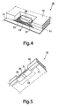
- FIG. 4 shows a third stage in the manufacture, after that a body 40 of electrically insulating material is provided.
- the body 40 comprises in this case an epoxy.
- FIGS. 5 and 6 shows the resulting device 10 , after that the first layer 12 has been removed.
- the component 20 is now kept in a mechanically stable manner in the device 10 through the presence of the attachment layer 13 that is partially overmolded and thus well maintained in the body 40 .
- the conductors 11 are herein present at the surface of the body, and may be include further contact pads for coupling to external components or an external board. Alternatively, an antenna or a flex foil may be present. It will be understood that the body as a whole can again be encapsulated in a further mould with any desired shape.
Applications Claiming Priority (3)
| Application Number | Priority Date | Filing Date | Title |
|---|---|---|---|
| EP03103824 | 2003-10-15 | ||
| EP03103824.3 | 2003-10-15 | ||
| PCT/IB2004/052051 WO2005039260A1 (en) | 2003-10-15 | 2004-10-11 | Electronic device and method of manufacturing thereof |
Publications (2)
| Publication Number | Publication Date |
|---|---|
| US20070075034A1 US20070075034A1 (en) | 2007-04-05 |
| US7433202B2 true US7433202B2 (en) | 2008-10-07 |
Family
ID=34443022
Family Applications (1)
| Application Number | Title | Priority Date | Filing Date |
|---|---|---|---|
| US10/575,582 Active 2024-12-14 US7433202B2 (en) | 2003-10-15 | 2004-10-11 | Electronic device and method of manufacturing thereof |
Country Status (6)
| Country | Link |
|---|---|
| US (1) | US7433202B2 (de) |
| EP (1) | EP1676471B1 (de) |
| JP (1) | JP5068075B2 (de) |
| CN (1) | CN100566507C (de) |
| AT (1) | ATE511744T1 (de) |
| WO (1) | WO2005039260A1 (de) |
Families Citing this family (3)
| Publication number | Priority date | Publication date | Assignee | Title |
|---|---|---|---|---|
| DE102006059127A1 (de) * | 2006-09-25 | 2008-03-27 | Osram Opto Semiconductors Gmbh | Verfahren zur Herstellung einer Anordnung optoelektronischer Bauelemente und Anordnung optoelektronischer Bauelemente |
| DE102009008738A1 (de) | 2009-02-12 | 2010-08-19 | Osram Opto Semiconductors Gmbh | Halbleiteranordnung und Verfahren zum Herstellen einer Halbleiteranordnung |
| EP3065514A4 (de) * | 2013-10-30 | 2017-04-26 | Kyocera Corporation | Leiterplatte und montagestruktur damit |
Citations (4)
| Publication number | Priority date | Publication date | Assignee | Title |
|---|---|---|---|---|
| US5013900A (en) * | 1982-12-28 | 1991-05-07 | Gao Gesellschaft Fur Automation Und Organisation Mbh | Identification card with integrated circuit |
| US5677568A (en) * | 1991-12-26 | 1997-10-14 | Mitsubishi Denki Kabushiki Kaisha | Thin IC card |
| US20030169575A1 (en) * | 2002-02-26 | 2003-09-11 | Kyocera Corporation | High frequency module |
| US7084935B2 (en) * | 2002-08-28 | 2006-08-01 | Adaptive Micro Systems, Llc | Display device with molded light guide |
Family Cites Families (11)
| Publication number | Priority date | Publication date | Assignee | Title |
|---|---|---|---|---|
| DE4141775A1 (de) * | 1991-12-18 | 1993-06-24 | Manfred Band | Verfahren zur herstellung einer elektronischen schaltung |
| US5723363A (en) * | 1995-09-29 | 1998-03-03 | Siemens Components, Inc. | Method of manufacturing a semiconductor device |
| DE19708615C1 (de) * | 1997-03-03 | 1998-07-23 | Siemens Ag | Chipkartenmodul und diesen umfassende Chipkarte |
| JP3699609B2 (ja) * | 1999-04-28 | 2005-09-28 | 京セラ株式会社 | 電子部品搭載用基板 |
| JP2001077277A (ja) * | 1999-09-03 | 2001-03-23 | Sony Corp | 半導体パッケージおよび半導体パッケージ製造方法 |
| JP2002270901A (ja) * | 2001-03-12 | 2002-09-20 | Citizen Electronics Co Ltd | 発光ダイオードとその製造方法 |
| EP1436773A1 (de) * | 2001-10-09 | 2004-07-14 | NagraID S.A. | Elektronisches modul mit einem schutzhöcker |
| FR2833801B1 (fr) * | 2001-12-19 | 2005-07-01 | Oberthur Card Syst Sa | Procede de realisation d'une carte a microcircuit |
| US6674652B2 (en) * | 2002-01-29 | 2004-01-06 | 3Com Corporation | Integrated shield wrap |
| DE10320990A1 (de) * | 2003-05-09 | 2004-11-25 | Dr. Johannes Heidenhain Gmbh | Induktiver Drehwinkelsensor und damit ausgestatteter Drehgeber |
| JP4433909B2 (ja) * | 2004-07-07 | 2010-03-17 | Tdk株式会社 | 表面実装型電子部品 |
-
2004
- 2004-10-11 AT AT04770224T patent/ATE511744T1/de not_active IP Right Cessation
- 2004-10-11 EP EP04770224A patent/EP1676471B1/de not_active Not-in-force
- 2004-10-11 US US10/575,582 patent/US7433202B2/en active Active
- 2004-10-11 JP JP2006534885A patent/JP5068075B2/ja not_active Expired - Fee Related
- 2004-10-11 WO PCT/IB2004/052051 patent/WO2005039260A1/en active Application Filing
- 2004-10-11 CN CNB2004800300617A patent/CN100566507C/zh not_active Expired - Fee Related
Patent Citations (4)
| Publication number | Priority date | Publication date | Assignee | Title |
|---|---|---|---|---|
| US5013900A (en) * | 1982-12-28 | 1991-05-07 | Gao Gesellschaft Fur Automation Und Organisation Mbh | Identification card with integrated circuit |
| US5677568A (en) * | 1991-12-26 | 1997-10-14 | Mitsubishi Denki Kabushiki Kaisha | Thin IC card |
| US20030169575A1 (en) * | 2002-02-26 | 2003-09-11 | Kyocera Corporation | High frequency module |
| US7084935B2 (en) * | 2002-08-28 | 2006-08-01 | Adaptive Micro Systems, Llc | Display device with molded light guide |
Also Published As
| Publication number | Publication date |
|---|---|
| EP1676471B1 (de) | 2011-06-01 |
| ATE511744T1 (de) | 2011-06-15 |
| JP2007508707A (ja) | 2007-04-05 |
| CN100566507C (zh) | 2009-12-02 |
| EP1676471A1 (de) | 2006-07-05 |
| CN1868243A (zh) | 2006-11-22 |
| US20070075034A1 (en) | 2007-04-05 |
| JP5068075B2 (ja) | 2012-11-07 |
| WO2005039260A1 (en) | 2005-04-28 |
Similar Documents
| Publication | Publication Date | Title |
|---|---|---|
| EP1168461B1 (de) | Lichtquelle | |
| US6528869B1 (en) | Semiconductor package with molded substrate and recessed input/output terminals | |
| RU2297736C2 (ru) | Способ встраивания компонента в основание и формирования электрического контакта с компонентом | |
| US6890829B2 (en) | Fabrication of on-package and on-chip structure using build-up layer process | |
| US7095054B2 (en) | Semiconductor package having light sensitive chips | |
| US6972964B2 (en) | Module board having embedded chips and components and method of forming the same | |
| KR0182073B1 (ko) | 반도체 칩 스케일 반도체 패키지 및 그 제조방법 | |
| KR100206049B1 (ko) | 가소 성형 집적 회로 패키지 | |
| US7732829B2 (en) | Optoelectronic device submount | |
| EP1253650A2 (de) | Oberflächenmontierbare Leuchtdiode | |
| US20020063340A1 (en) | Semiconductor device and method for producing the same | |
| KR101149645B1 (ko) | 광커플러 장치들 | |
| US20060261450A1 (en) | Leadframeless package structure and method | |
| US6458627B1 (en) | Semiconductor chip package and method of fabricating same | |
| US8269354B2 (en) | Semiconductor package substrate structure and manufacturing method thereof | |
| CN111433906A (zh) | 一种内部电源焊盘间距更小的半导体封装 | |
| CN110600440A (zh) | 一种埋入式封装结构及其制备方法、终端 | |
| KR20050084417A (ko) | 전자 장치, 그 제조 방법 및 호일 | |
| US7433202B2 (en) | Electronic device and method of manufacturing thereof | |
| US20020149121A1 (en) | Base interconnection substrate, manufacturing method thereof, semiconductor device and manfacturing method thereof | |
| US20060087010A1 (en) | IC substrate and manufacturing method thereof and semiconductor element package thereby | |
| KR19980068343A (ko) | 가요성 회로 기판을 이용한 칩 스케일 반도체 패키지 및 그 제조 방법 | |
| KR100388297B1 (ko) | 반도체패키지용 회로기판의 솔더마스크 라미네이션 방법 | |
| TW202322224A (zh) | 混合嵌埋封裝結構及其製作方法 | |
| KR100763963B1 (ko) | 티비지에이 반도체 패키지용 기판과 이의 제조방법 |
Legal Events
| Date | Code | Title | Description |
|---|---|---|---|
| AS | Assignment |
Owner name: KONINKLIJKE PHILIPS ELECTRONICS, N.V., NETHERLANDS Free format text: ASSIGNMENT OF ASSIGNORS INTEREST;ASSIGNORS:VAN MONTFORT, VINCENT JOHANNES;VERWEG, FRANSISCUS GERARDUS COENRADUS;KUSTERS, ROEL HENRI LOUIS;REEL/FRAME:017799/0219 Effective date: 20050512 |
|
| STCF | Information on status: patent grant |
Free format text: PATENTED CASE |
|
| AS | Assignment |
Owner name: CHIMEI INNOLUX CORPORATION, TAIWAN Free format text: ASSIGNMENT OF ASSIGNORS INTEREST;ASSIGNOR:KONINKLIJKE PHILIPS ELECTRONICS N.V.;REEL/FRAME:025407/0964 Effective date: 20100927 |
|
| FPAY | Fee payment |
Year of fee payment: 4 |
|
| AS | Assignment |
Owner name: INNOLUX CORPORATION, TAIWAN Free format text: CHANGE OF NAME;ASSIGNOR:CHIMEI INNOLUX CORPORATION;REEL/FRAME:032604/0487 Effective date: 20121219 |
|
| FPAY | Fee payment |
Year of fee payment: 8 |
|
| AS | Assignment |
Owner name: VIDA SENSE INNOVATION LTD., SAMOA Free format text: ASSIGNMENT OF ASSIGNORS INTEREST;ASSIGNOR:INNOLUX CORPORATION;REEL/FRAME:049938/0689 Effective date: 20190724 |
|
| MAFP | Maintenance fee payment |
Free format text: PAYMENT OF MAINTENANCE FEE, 12TH YEAR, LARGE ENTITY (ORIGINAL EVENT CODE: M1553); ENTITY STATUS OF PATENT OWNER: LARGE ENTITY Year of fee payment: 12 |
|
| IPR | Aia trial proceeding filed before the patent and appeal board: inter partes review |
Free format text: TRIAL NO: IPR2022-00109 Opponent name: HKC CORPORATION LIMITED, HKC OVERSEAS LIMITED, CHONGQING HKC OPTOELECTRONICS TECHNOLOGY CO., ELEMENT ELECTRONICS HOLDINGS, LLC, SCEPTRE INC., AND TINNOVATE LLC Effective date: 20211028 |