US7428686B2 - Error detection/correction system, and controller using this system - Google Patents
Error detection/correction system, and controller using this system Download PDFInfo
- Publication number
- US7428686B2 US7428686B2 US10/726,561 US72656103A US7428686B2 US 7428686 B2 US7428686 B2 US 7428686B2 US 72656103 A US72656103 A US 72656103A US 7428686 B2 US7428686 B2 US 7428686B2
- Authority
- US
- United States
- Prior art keywords
- error detection
- correction
- data
- error
- modules
- Prior art date
- Legal status (The legal status is an assumption and is not a legal conclusion. Google has not performed a legal analysis and makes no representation as to the accuracy of the status listed.)
- Expired - Lifetime, expires
Links
- 238000012937 correction Methods 0.000 title claims abstract description 133
- 238000001514 detection method Methods 0.000 title claims abstract description 121
- 238000012546 transfer Methods 0.000 claims description 20
- 230000005540 biological transmission Effects 0.000 claims description 13
- 230000001419 dependent effect Effects 0.000 claims description 10
- 238000007689 inspection Methods 0.000 claims description 9
- 238000010586 diagram Methods 0.000 description 4
- 230000006870 function Effects 0.000 description 3
- 238000004891 communication Methods 0.000 description 1
- 230000010485 coping Effects 0.000 description 1
- 238000000034 method Methods 0.000 description 1
- 238000004321 preservation Methods 0.000 description 1
- 238000012545 processing Methods 0.000 description 1
Images


Classifications
-
- H—ELECTRICITY
- H04—ELECTRIC COMMUNICATION TECHNIQUE
- H04L—TRANSMISSION OF DIGITAL INFORMATION, e.g. TELEGRAPHIC COMMUNICATION
- H04L1/00—Arrangements for detecting or preventing errors in the information received
- H04L1/004—Arrangements for detecting or preventing errors in the information received by using forward error control
- H04L1/0045—Arrangements at the receiver end
-
- H—ELECTRICITY
- H04—ELECTRIC COMMUNICATION TECHNIQUE
- H04L—TRANSMISSION OF DIGITAL INFORMATION, e.g. TELEGRAPHIC COMMUNICATION
- H04L1/00—Arrangements for detecting or preventing errors in the information received
- H04L1/004—Arrangements for detecting or preventing errors in the information received by using forward error control
- H04L1/0041—Arrangements at the transmitter end
-
- H—ELECTRICITY
- H04—ELECTRIC COMMUNICATION TECHNIQUE
- H04L—TRANSMISSION OF DIGITAL INFORMATION, e.g. TELEGRAPHIC COMMUNICATION
- H04L1/00—Arrangements for detecting or preventing errors in the information received
- H04L2001/0092—Error control systems characterised by the topology of the transmission link
- H04L2001/0094—Bus
-
- H—ELECTRICITY
- H04—ELECTRIC COMMUNICATION TECHNIQUE
- H04L—TRANSMISSION OF DIGITAL INFORMATION, e.g. TELEGRAPHIC COMMUNICATION
- H04L1/00—Arrangements for detecting or preventing errors in the information received
- H04L2001/0098—Unequal error protection
Definitions
- the present invention relates to an error detection/correction system and a controller using this system in a bus that connects modules of the control system with each other.
- the data may include an error during the transmission.
- error detection/correction codes are used. In general, if an error detection/correction code has more inspection bits, then the detection/correction capacity becomes higher. If the unit for error detection/correction becomes larger, then the detection/correction capacity becomes higher when the ratio of the number of inspection bits to the number of information bits is the same.
- the address and command portions of the bus transfer unit have a fixed length, while the data portion has a variable length. From this constraint, the size of a packet for error detection/correction is determined based on the minimum transfer quantity on a data side. In general, detection/correction capacity depends on ratio of inspection bits to information bits.
- a data error detection device (refer to Japanese Patent Application Laid-open No. 11-65944) in which, for coping with a variation in data quantity to be transmitted and received, a plurality of (k) ECC (error correction code) circuits (of n bits), which has been used when the number of output bits of the memory element is small, are used to detect an occurrence of trouble in the memory element, when the number of output bits of a memory element increases (to n ⁇ k bits).
- ECC error correction code
- each terminal unit In multiple starting points/multiple targets terminal unit switching system that exchanges messages via a fixed size burst or a cell, there is known a system in which each terminal unit generates an initial error correction code in a first burst of a message, a preceding burst error correction code, and an error correction code as a function of a burst data byte, and detects an error by comparing these generated error correction codes with a reception burst error correction code, thereby to secure the preservation of message exchanged between data processing terminals (refer to Japanese Patent Application Laid-open No. 6-53942).
- the detection/correction capacity becomes constant.
- the unit for error detection/correction becomes large, it is not possible to obtain the above-explained merit that, if the ratio of the number of inspection bits to the number of information bits is the same, the detection/correction capacity becomes higher when the unit for error detection/correction becomes larger.
- a plurality of error detection/correction code generation circuits having a difference in at least one of an inspection bit length, an information bit length, and a correction capacity, and error detection/correction circuits corresponding to the error detection/correction code generation circuits are built into the system, and an error detection/correction code generation circuit and an error detection/correction circuit to be used are switched over dependent upon a kind, a length, and a timing of the data to be transferred.
- the error detection/correction system according to the present invention may adopt the following embodiments.
- the error detection/correction system may switch over error detection/correction codes to be used dependent upon a phase of transmitting an address, a command, and data.
- the error detection/correction system may switch over error detection/correction codes to be used, dependent upon whether in a single access mode or in a burst access mode.
- the error detection/correction system may switch over error detection/correction codes to be used, dependent upon a data quantity to be transferred.
- the controller according to the present invention may have a plurality of modules, connected via buses, adopting the above error detection/correction system.
- the controller may comprise a serial transfer module that connects a plurality buses connecting the plurality of modules, by means of a serial transmission line, wherein a plurality of error detection/correction code generation circuits having a difference in at least one of an inspection bit length, an information bit length, and a correction capacity, and error detection/correction circuits corresponding to the error detection/correction code generation circuits are also built into the serial transfer module, and the error detection/correction system is used also in the serial transfer.
- an error detection/correction system and a controller that employs this system both capable of improving the correction/detection capacity to obtain an optimum capacity even when the size of a unit for error detection/correction changes and for any kind of information.
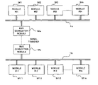
- FIG. 1 is a block diagram of a main portion of a controller employing the error detection/correction system according to one embodiment of the present invention
- FIGS. 2A to 2C are explanatory diagrams of transfer formats on buses according to the embodiment.
- FIG. 3 is a block diagram of a main portion of a module according to the embodiment.
- FIG. 1 is a block diagram of a main portion of a controller employing the error detection/correction system according to one embodiment of the present invention.
- a plurality of modules M 1 to Mn are connected to a bus 1 a .
- a plurality of modules M 11 to M 1 n are also connected to a bus 1 b .
- the bus 1 a and the bus 1 b are connected to each other in series via bus connection modules Ma and Mb.
- Each module can become a bus master or a bus slave.
- the bus master When a bus master obtains a right of using a bus, the bus master outputs an address of an access destination and a command, so that a bus cycle is generated. A state where these pieces of information are output is called address phase.
- a module other than the bus master receives the information of the address phase, and when the module finds that the access is made to the self, this module becomes a slave, with the result that data exchange between the bus master and the bus slave is carried out.
- a state where the data exchange is carried out is called data phase.
- FIGS. 2A to 2C illustrate transfer formats on buses.
- an address phase an address and a command are transmitted sequentially, and an error correction code (hereinafter referred to as ECC code) is added last to the whole of the address and command.
- ECC code error correction code
- an ECC code may be added to each of the address and the command, the format of address phase is fixed in any case.
- the data phase there are single access in which a data quantity is fixed as shown in FIG. 2A and FIG. 2B , and a burst access in which a data quantity is variable as shown in FIG. 2C .
- the ECC code is added to 32 bits of a data quantity as shown in FIG. 2A .
- the ECC code is added to 64 bits of a data quantity as shown in FIG. 2B .
- the burst access as a data quantity is variable, and data and the ECC code are not isolated, as shown in FIG. 2C .
- the information indicating a difference of a format of data phase is contained in the command of address phase.
- a slave decides the format of data phase based on this information.
- FIG. 3 illustrates a configuration inside the module.
- the modules M 1 to Mn and M 11 to M 1 n can become both bus masters and slaves.
- the bus connection modules Ma and Mb also have the same configuration as the configuration of these modules.
- FIG. 3 illustrates the configuration of one module (M is assigned to represent the modules M 1 to Mn and M 11 to M 1 n , and the bus connection modules Ma and Mb).
- Each module M has a transmitter 10 and a receiver 11 .
- the transmitter 10 and the receiver 11 are connected to an inter-module bus ( 1 a , 1 b ) or a serial transmission line via an internal bus 12 .
- the transmitter 10 comprises: a detection/correction code generation circuit #A that receives an address/command to generate an error detection/correction code (ECC code); a detection/correction code generation circuit #B that receives data of single 32 bits to generate an error detection/correction code (ECC code); a detection/correction code generation circuit #C that receives data of single 64 bits of a double data width to generate an error detection/correction code (ECC code); a detection/correction code generation circuit #D that receives burst data to generates an error detection/correction code (ECC code); and a transmitter selection circuit 13 .
- ECC code error detection/correction code
- a detection/correction code generation circuit #B that receives data of single 32 bits to generate an error detection/correction code
- ECC code generation circuit #C that receives data of single 64 bits of a double data width to generate an error detection/correction code
- ECC code generation circuit #D that receives burst data to generate
- the address, command, and data are transmitted to the internal bus 12 respectively.
- the transmitter selection circuit 13 adds the ECC code as shown in FIG. 2A to FIG. 2C to the data according to address/command and a kind of data transmitted.
- the address/command and data to which an ECC code is added is transmitted to either the inter-module buses 1 a , 1 b or the serial transmission line.
- the receiver 11 comprises: a receiver selection circuit 14 ; an error detection/correction circuit #A that detects and corrects an error of address/command; an error detection/correction circuit #B that detects and corrects an error of data of single 32 bits; an error detection/correction circuit #C that detects and corrects an error of data of single 64 bits of a double data width; and an error detection/correction circuit #D that detects and corrects an error of burst data.
- the receiver selection circuit 14 delivers the data to the error detection/correction circuits #A to #D according to address/command and a kind of data received via either the inter-module buses 1 a , 1 b or the serial transmission line.
- the error detection/correction circuits #A to #D detect and correct errors, and the address/command and data for which error detection/correction is completed is delivered in the module M.
- the transmitter selection circuit 13 selects the ECC code generated by the detection/correction code generation circuit #A for the address/command phase.
- the ECC code is added to the last of the address/command as shown in FIG. 2 , and the address/command to which the ECC code is added is transmitted to either the inter-module buses 1 a , 1 b or the serial transmission line.
- the receiver selection circuit 14 selects the error detection/correction circuit #A for the address phase when receiving the address phase.
- the slave transmits data to read the data
- the bus master transmits data to write the data.
- the transmitter module switches over between the detection/correction code generation circuits #A to #D on the side of the transmitter 10 for each transfer format as shown in FIG. 2A to FIG. 2C , and transmits the switched result to the bus.
- the receiver selection circuit 14 selectively switches over between error detection/correction circuits #A to #D on the side of the receiver correspondingly.
- the receiver slave module When the bus master outputs address/command to write data, the receiver slave module recognizes the transfer format based on the information of the command received in the address phase. Based on the transfer format instructed by this command, the receiver selection circuit 14 of the receiver module (slave) receives the data by switching over the circuit to the error detection/correction circuit #B in case where the data is single 32 bits, by switching over the circuit to the error detection/correction circuit #C in case where the data is single 64 bits, or by switching over the circuit to the error detection/correction circuit #D in case where the data is burst data.
- the receiver slave module recognizes the transfer format based on the information of the command received in the address phase. Based on this transfer format, the transmitter selection circuit 13 switches over between the detection/correction code generation circuits #B to #D to transmit the read data to which the ECC code generated in the detection/correction code generation circuits #B to #D is added, as shown in FIG. 2 .
- the module of the bus master that receives this data has already assigned the transfer format when transmitting the address/command in the address phase. Therefore, the receiver selection circuit 14 of the module of this bus master selectively switches over between the error detection/correction circuits #B to #D corresponding to the assigned transfer format, and detects and corrects the error of the received data, and takes in the data.
- the error detection/correction code generation circuits or the error detection/correction circuits are switched over so that an optimum circuit carries out error detection and correction.
- each module in the communication between modules that are connected to each other via buses in the controller, each module has detection/correction code generation circuits and error detection/correction circuits corresponding to a few kinds of transfer formats. With this arrangement, optimum data transmission can be achieved.
- a module comprises an error detection/correction code generation circuit #A and an error detection/correction circuit #A for address/command, an error detection/correction code generation circuit #B and an error detection/correction circuit #B for single 32 bit data, an error detection/correction code generation circuit #C and an error detection/correction circuit #C for single 64 bit data, and an error detection/correction code generation circuit #D and an error detection/correction circuit #D for burst data.
- it is also possible to employ a necessary optimum error detection/correction system by providing error detection/correction code generation circuits and error detection/correction circuits having a difference in inspection bit length, information bit length, and correction capacity.
- error detection/correction is carried out in a large packet unit for the address and command portions having a fixed length.
- the detection and correction capacity for the address and command portions can be increased, as compared with the capacity for the data portion.
- a cause and a trouble portion of the inconvenience can easily be identified. For example, when adjacent two bit error detection is applied to address/command portion, and one bit error detection is applied to data transfer portion, although the system cannot continue operating when adjacent two bits of bus are short-circuited, it is possible to identify which of two bits of the bus are in trouble, so that it is effective in analyzing a trouble portion and a cause.
- an optimum function is used for data transmitting according to the contents, quantity and characteristics of information to be transmitted. Therefore, it is possible to achieve highly reliable data transmission.
Landscapes
- Engineering & Computer Science (AREA)
- Computer Networks & Wireless Communication (AREA)
- Signal Processing (AREA)
- Detection And Correction Of Errors (AREA)
- Detection And Prevention Of Errors In Transmission (AREA)
- Error Detection And Correction (AREA)
Applications Claiming Priority (3)
| Application Number | Priority Date | Filing Date | Title |
|---|---|---|---|
| JP355634/2002 | 2002-12-06 | ||
| JP2002-355634 | 2002-12-06 | ||
| JP2002355634A JP3757204B2 (ja) | 2002-12-06 | 2002-12-06 | エラー検出/訂正方式及び該方式を用いた制御装置 |
Publications (2)
| Publication Number | Publication Date |
|---|---|
| US20040153939A1 US20040153939A1 (en) | 2004-08-05 |
| US7428686B2 true US7428686B2 (en) | 2008-09-23 |
Family
ID=32310768
Family Applications (1)
| Application Number | Title | Priority Date | Filing Date |
|---|---|---|---|
| US10/726,561 Expired - Lifetime US7428686B2 (en) | 2002-12-06 | 2003-12-04 | Error detection/correction system, and controller using this system |
Country Status (3)
| Country | Link |
|---|---|
| US (1) | US7428686B2 (ja) |
| EP (1) | EP1427126B1 (ja) |
| JP (1) | JP3757204B2 (ja) |
Cited By (2)
| Publication number | Priority date | Publication date | Assignee | Title |
|---|---|---|---|---|
| US20060236196A1 (en) * | 2005-03-31 | 2006-10-19 | Vogt Pete D | Combined command and data code |
| US20090013108A1 (en) * | 2005-01-31 | 2009-01-08 | Intel Corporation | Memory buffers for merging local data from memory modules |
Families Citing this family (10)
| Publication number | Priority date | Publication date | Assignee | Title |
|---|---|---|---|---|
| EP1880498B1 (en) * | 2005-05-13 | 2012-07-11 | Fisher-Rosemount Systems, Inc. | Fieldbus process communications using error correction |
| JP4226620B2 (ja) * | 2006-08-24 | 2009-02-18 | ファナック株式会社 | データ転送方式及びデータ転送装置 |
| FR2917863A1 (fr) * | 2007-06-20 | 2008-12-26 | St Microelectronics Crolles 2 | Bus avec circuit de correction d'erreur |
| TW201201008A (en) | 2010-03-22 | 2012-01-01 | Mosaid Technologies Inc | Composite semiconductor memory device with error correction |
| JP2012257122A (ja) * | 2011-06-09 | 2012-12-27 | Hitachi Automotive Systems Ltd | 車両制御装置、車両制御システム |
| JP2013062691A (ja) * | 2011-09-13 | 2013-04-04 | Dainippon Printing Co Ltd | 情報処理装置及びコンピュータプログラム |
| KR101829464B1 (ko) * | 2011-10-13 | 2018-04-11 | 삼성전자주식회사 | 패킷 데이터의 인코딩 방법 및 장치 |
| CN108197199B (zh) * | 2017-12-27 | 2021-10-29 | 珠海市君天电子科技有限公司 | 数据监控方法、装置、电子设备及计算机可读存储介质 |
| JP7428689B2 (ja) | 2021-12-17 | 2024-02-06 | 華邦電子股▲ふん▼有限公司 | メモリシステム |
| KR102645215B1 (ko) * | 2022-01-27 | 2024-03-07 | 윈본드 일렉트로닉스 코포레이션 | 메모리 시스템 |
Citations (16)
| Publication number | Priority date | Publication date | Assignee | Title |
|---|---|---|---|---|
| US4356550A (en) * | 1976-09-07 | 1982-10-26 | Tandem Computers Incorporated | Multiprocessor system |
| US4453213A (en) * | 1981-07-30 | 1984-06-05 | Harris Corporation | Error reporting scheme |
| JPH05158808A (ja) | 1991-12-06 | 1993-06-25 | Nec Eng Ltd | マイクロプログラム制御装置 |
| US5260951A (en) | 1991-05-24 | 1993-11-09 | Sony Corporation | Error correction circuit for digital data |
| EP0647035A1 (en) | 1993-09-30 | 1995-04-05 | Victor Company Of Japan, Limited | Method of processing code for error checking and code processing circuit |
| JPH0853942A (ja) | 1994-08-12 | 1996-02-27 | Fujita Corp | Pc床板用吊り治具及びこの治具によるpc床板の敷設方法 |
| US5535405A (en) * | 1993-12-23 | 1996-07-09 | Unisys Corporation | Microsequencer bus controller system |
| US5539754A (en) * | 1992-10-05 | 1996-07-23 | Hewlett-Packard Company | Method and circuitry for generating syndrome bits within an error correction and detection circuit |
| US5570425A (en) * | 1994-11-07 | 1996-10-29 | Digisonix, Inc. | Transducer daisy chain |
| US5638384A (en) | 1993-01-07 | 1997-06-10 | Kabushiki Kaisha Toshiba | Data communication system |
| US5701413A (en) * | 1993-01-25 | 1997-12-23 | Bull Hn Information Systems Italia S.P.A. | Multi-processor system with shared memory |
| WO1998001806A1 (fr) | 1996-07-03 | 1998-01-15 | Hitachi, Ltd. | Processeur d'informations |
| JPH1165944A (ja) | 1997-08-13 | 1999-03-09 | Fujitsu Ltd | データ誤り検出装置 |
| US6282688B1 (en) * | 1991-09-20 | 2001-08-28 | Hitachi, Ltd. | Recording apparatus |
| US20020138794A1 (en) * | 1995-09-29 | 2002-09-26 | Yoshihiro Kikuchi | Coding system and decoding system |
| US6745268B1 (en) * | 2000-08-11 | 2004-06-01 | Micron Technology, Lnc. | Capacitive multidrop bus compensation |
-
2002
- 2002-12-06 JP JP2002355634A patent/JP3757204B2/ja not_active Expired - Fee Related
-
2003
- 2003-12-03 EP EP03257609A patent/EP1427126B1/en not_active Expired - Lifetime
- 2003-12-04 US US10/726,561 patent/US7428686B2/en not_active Expired - Lifetime
Patent Citations (16)
| Publication number | Priority date | Publication date | Assignee | Title |
|---|---|---|---|---|
| US4356550A (en) * | 1976-09-07 | 1982-10-26 | Tandem Computers Incorporated | Multiprocessor system |
| US4453213A (en) * | 1981-07-30 | 1984-06-05 | Harris Corporation | Error reporting scheme |
| US5260951A (en) | 1991-05-24 | 1993-11-09 | Sony Corporation | Error correction circuit for digital data |
| US6282688B1 (en) * | 1991-09-20 | 2001-08-28 | Hitachi, Ltd. | Recording apparatus |
| JPH05158808A (ja) | 1991-12-06 | 1993-06-25 | Nec Eng Ltd | マイクロプログラム制御装置 |
| US5539754A (en) * | 1992-10-05 | 1996-07-23 | Hewlett-Packard Company | Method and circuitry for generating syndrome bits within an error correction and detection circuit |
| US5638384A (en) | 1993-01-07 | 1997-06-10 | Kabushiki Kaisha Toshiba | Data communication system |
| US5701413A (en) * | 1993-01-25 | 1997-12-23 | Bull Hn Information Systems Italia S.P.A. | Multi-processor system with shared memory |
| EP0647035A1 (en) | 1993-09-30 | 1995-04-05 | Victor Company Of Japan, Limited | Method of processing code for error checking and code processing circuit |
| US5535405A (en) * | 1993-12-23 | 1996-07-09 | Unisys Corporation | Microsequencer bus controller system |
| JPH0853942A (ja) | 1994-08-12 | 1996-02-27 | Fujita Corp | Pc床板用吊り治具及びこの治具によるpc床板の敷設方法 |
| US5570425A (en) * | 1994-11-07 | 1996-10-29 | Digisonix, Inc. | Transducer daisy chain |
| US20020138794A1 (en) * | 1995-09-29 | 2002-09-26 | Yoshihiro Kikuchi | Coding system and decoding system |
| WO1998001806A1 (fr) | 1996-07-03 | 1998-01-15 | Hitachi, Ltd. | Processeur d'informations |
| JPH1165944A (ja) | 1997-08-13 | 1999-03-09 | Fujitsu Ltd | データ誤り検出装置 |
| US6745268B1 (en) * | 2000-08-11 | 2004-06-01 | Micron Technology, Lnc. | Capacitive multidrop bus compensation |
Non-Patent Citations (1)
| Title |
|---|
| Notice of Reasons for Rejection. |
Cited By (4)
| Publication number | Priority date | Publication date | Assignee | Title |
|---|---|---|---|---|
| US20090013108A1 (en) * | 2005-01-31 | 2009-01-08 | Intel Corporation | Memory buffers for merging local data from memory modules |
| US8166218B2 (en) | 2005-01-31 | 2012-04-24 | Intel Corporation | Memory buffers for merging local data from memory modules |
| US20060236196A1 (en) * | 2005-03-31 | 2006-10-19 | Vogt Pete D | Combined command and data code |
| US7827462B2 (en) * | 2005-03-31 | 2010-11-02 | Intel Corporation | Combined command and data code |
Also Published As
| Publication number | Publication date |
|---|---|
| EP1427126B1 (en) | 2011-11-16 |
| JP2004193664A (ja) | 2004-07-08 |
| JP3757204B2 (ja) | 2006-03-22 |
| US20040153939A1 (en) | 2004-08-05 |
| EP1427126A3 (en) | 2006-10-04 |
| EP1427126A2 (en) | 2004-06-09 |
Similar Documents
| Publication | Publication Date | Title |
|---|---|---|
| US5799245A (en) | Cooperative diversity antenna switching on transmitter and receiver side | |
| CA2115730C (en) | Data transmission method and system therefor | |
| US7428686B2 (en) | Error detection/correction system, and controller using this system | |
| US20040153952A1 (en) | CRC encoding scheme for conveying status information | |
| EP1014273A2 (en) | Method of start/stop synchronous data transmission | |
| US5537535A (en) | Multi-CPU system having fault monitoring facility | |
| US9479277B2 (en) | Mechanism for channel synchronization | |
| EP0193928B1 (en) | Method of processing abnormal situation in digital transmission system | |
| US6697966B1 (en) | Data bus for a plurality of nodes | |
| WO2005066821A2 (en) | Using feedback to select transmitting voltage | |
| WO1996037984A1 (en) | A digital data bus system including arbitration | |
| US6026094A (en) | Digital data bus system including arbitration | |
| US5384778A (en) | Communication control apparatus | |
| US6078962A (en) | Bi-directional asynchronous transfer scheme using a single handshake | |
| JP4612640B2 (ja) | データ通信システムおよびデータ通信方法 | |
| US5784367A (en) | Method and device for communications between plural terminals, compatible with the ARINC 629 standard | |
| US20030021390A1 (en) | Device for connection of a device on a telephone line | |
| US5267250A (en) | Circuit arrangement for detection of an erroneous selection signal supplied to selection means | |
| US5793841A (en) | Apparatus and method for receiving dual highway data in electronic switching system | |
| KR20080013973A (ko) | 통신 시스템의 적어도 2개의 가입자들 간의 통신을 위한방법 | |
| US6944176B1 (en) | Method and apparatus for bit level network data multiplexing | |
| JPH07264212A (ja) | 警報情報転送方式 | |
| JP2002094535A (ja) | エラーコード送出装置および方法 | |
| KR20000042931A (ko) | 보드내 오류의 우선 순위에 따른 이중화 절체 방법 | |
| JP2002073430A (ja) | エラー・メッセージを送信するための装置および方法 |
Legal Events
| Date | Code | Title | Description |
|---|---|---|---|
| AS | Assignment |
Owner name: FANUC LTD., JAPAN Free format text: ASSIGNMENT OF ASSIGNORS INTEREST;ASSIGNORS:AOYAMA, KAZUNARI;NAKAMURA, MINORU;SAKAI, YUTAKA;REEL/FRAME:014760/0633;SIGNING DATES FROM 20031119 TO 20031125 |
|
| STCF | Information on status: patent grant |
Free format text: PATENTED CASE |
|
| CC | Certificate of correction | ||
| FEPP | Fee payment procedure |
Free format text: PAYOR NUMBER ASSIGNED (ORIGINAL EVENT CODE: ASPN); ENTITY STATUS OF PATENT OWNER: LARGE ENTITY |
|
| FPAY | Fee payment |
Year of fee payment: 4 |
|
| FPAY | Fee payment |
Year of fee payment: 8 |
|
| MAFP | Maintenance fee payment |
Free format text: PAYMENT OF MAINTENANCE FEE, 12TH YEAR, LARGE ENTITY (ORIGINAL EVENT CODE: M1553); ENTITY STATUS OF PATENT OWNER: LARGE ENTITY Year of fee payment: 12 |