US7403176B2 - Image display device, and display panel and driving method thereof, and pixel circuit - Google Patents
Image display device, and display panel and driving method thereof, and pixel circuit Download PDFInfo
- Publication number
- US7403176B2 US7403176B2 US10/634,337 US63433703A US7403176B2 US 7403176 B2 US7403176 B2 US 7403176B2 US 63433703 A US63433703 A US 63433703A US 7403176 B2 US7403176 B2 US 7403176B2
- Authority
- US
- United States
- Prior art keywords
- transistor
- current
- control electrode
- coupled
- voltage
- Prior art date
- Legal status (The legal status is an assumption and is not a legal conclusion. Google has not performed a legal analysis and makes no representation as to the accuracy of the status listed.)
- Expired - Fee Related, expires
Links
Images




Classifications
-
- G—PHYSICS
- G09—EDUCATION; CRYPTOGRAPHY; DISPLAY; ADVERTISING; SEALS
- G09G—ARRANGEMENTS OR CIRCUITS FOR CONTROL OF INDICATING DEVICES USING STATIC MEANS TO PRESENT VARIABLE INFORMATION
- G09G3/00—Control arrangements or circuits, of interest only in connection with visual indicators other than cathode-ray tubes
- G09G3/20—Control arrangements or circuits, of interest only in connection with visual indicators other than cathode-ray tubes for presentation of an assembly of a number of characters, e.g. a page, by composing the assembly by combination of individual elements arranged in a matrix no fixed position being assigned to or needed to be assigned to the individual characters or partial characters
- G09G3/22—Control arrangements or circuits, of interest only in connection with visual indicators other than cathode-ray tubes for presentation of an assembly of a number of characters, e.g. a page, by composing the assembly by combination of individual elements arranged in a matrix no fixed position being assigned to or needed to be assigned to the individual characters or partial characters using controlled light sources
- G09G3/30—Control arrangements or circuits, of interest only in connection with visual indicators other than cathode-ray tubes for presentation of an assembly of a number of characters, e.g. a page, by composing the assembly by combination of individual elements arranged in a matrix no fixed position being assigned to or needed to be assigned to the individual characters or partial characters using controlled light sources using electroluminescent panels
-
- G—PHYSICS
- G09—EDUCATION; CRYPTOGRAPHY; DISPLAY; ADVERTISING; SEALS
- G09G—ARRANGEMENTS OR CIRCUITS FOR CONTROL OF INDICATING DEVICES USING STATIC MEANS TO PRESENT VARIABLE INFORMATION
- G09G3/00—Control arrangements or circuits, of interest only in connection with visual indicators other than cathode-ray tubes
- G09G3/20—Control arrangements or circuits, of interest only in connection with visual indicators other than cathode-ray tubes for presentation of an assembly of a number of characters, e.g. a page, by composing the assembly by combination of individual elements arranged in a matrix no fixed position being assigned to or needed to be assigned to the individual characters or partial characters
- G09G3/22—Control arrangements or circuits, of interest only in connection with visual indicators other than cathode-ray tubes for presentation of an assembly of a number of characters, e.g. a page, by composing the assembly by combination of individual elements arranged in a matrix no fixed position being assigned to or needed to be assigned to the individual characters or partial characters using controlled light sources
- G09G3/30—Control arrangements or circuits, of interest only in connection with visual indicators other than cathode-ray tubes for presentation of an assembly of a number of characters, e.g. a page, by composing the assembly by combination of individual elements arranged in a matrix no fixed position being assigned to or needed to be assigned to the individual characters or partial characters using controlled light sources using electroluminescent panels
- G09G3/32—Control arrangements or circuits, of interest only in connection with visual indicators other than cathode-ray tubes for presentation of an assembly of a number of characters, e.g. a page, by composing the assembly by combination of individual elements arranged in a matrix no fixed position being assigned to or needed to be assigned to the individual characters or partial characters using controlled light sources using electroluminescent panels semiconductive, e.g. using light-emitting diodes [LED]
- G09G3/3208—Control arrangements or circuits, of interest only in connection with visual indicators other than cathode-ray tubes for presentation of an assembly of a number of characters, e.g. a page, by composing the assembly by combination of individual elements arranged in a matrix no fixed position being assigned to or needed to be assigned to the individual characters or partial characters using controlled light sources using electroluminescent panels semiconductive, e.g. using light-emitting diodes [LED] organic, e.g. using organic light-emitting diodes [OLED]
- G09G3/3225—Control arrangements or circuits, of interest only in connection with visual indicators other than cathode-ray tubes for presentation of an assembly of a number of characters, e.g. a page, by composing the assembly by combination of individual elements arranged in a matrix no fixed position being assigned to or needed to be assigned to the individual characters or partial characters using controlled light sources using electroluminescent panels semiconductive, e.g. using light-emitting diodes [LED] organic, e.g. using organic light-emitting diodes [OLED] using an active matrix
- G09G3/3233—Control arrangements or circuits, of interest only in connection with visual indicators other than cathode-ray tubes for presentation of an assembly of a number of characters, e.g. a page, by composing the assembly by combination of individual elements arranged in a matrix no fixed position being assigned to or needed to be assigned to the individual characters or partial characters using controlled light sources using electroluminescent panels semiconductive, e.g. using light-emitting diodes [LED] organic, e.g. using organic light-emitting diodes [OLED] using an active matrix with pixel circuitry controlling the current through the light-emitting element
-
- G—PHYSICS
- G09—EDUCATION; CRYPTOGRAPHY; DISPLAY; ADVERTISING; SEALS
- G09G—ARRANGEMENTS OR CIRCUITS FOR CONTROL OF INDICATING DEVICES USING STATIC MEANS TO PRESENT VARIABLE INFORMATION
- G09G2300/00—Aspects of the constitution of display devices
- G09G2300/08—Active matrix structure, i.e. with use of active elements, inclusive of non-linear two terminal elements, in the pixels together with light emitting or modulating elements
- G09G2300/0809—Several active elements per pixel in active matrix panels
- G09G2300/0819—Several active elements per pixel in active matrix panels used for counteracting undesired variations, e.g. feedback or autozeroing
-
- G—PHYSICS
- G09—EDUCATION; CRYPTOGRAPHY; DISPLAY; ADVERTISING; SEALS
- G09G—ARRANGEMENTS OR CIRCUITS FOR CONTROL OF INDICATING DEVICES USING STATIC MEANS TO PRESENT VARIABLE INFORMATION
- G09G2300/00—Aspects of the constitution of display devices
- G09G2300/08—Active matrix structure, i.e. with use of active elements, inclusive of non-linear two terminal elements, in the pixels together with light emitting or modulating elements
- G09G2300/0809—Several active elements per pixel in active matrix panels
- G09G2300/0842—Several active elements per pixel in active matrix panels forming a memory circuit, e.g. a dynamic memory with one capacitor
-
- G—PHYSICS
- G09—EDUCATION; CRYPTOGRAPHY; DISPLAY; ADVERTISING; SEALS
- G09G—ARRANGEMENTS OR CIRCUITS FOR CONTROL OF INDICATING DEVICES USING STATIC MEANS TO PRESENT VARIABLE INFORMATION
- G09G2300/00—Aspects of the constitution of display devices
- G09G2300/08—Active matrix structure, i.e. with use of active elements, inclusive of non-linear two terminal elements, in the pixels together with light emitting or modulating elements
- G09G2300/0809—Several active elements per pixel in active matrix panels
- G09G2300/0842—Several active elements per pixel in active matrix panels forming a memory circuit, e.g. a dynamic memory with one capacitor
- G09G2300/0861—Several active elements per pixel in active matrix panels forming a memory circuit, e.g. a dynamic memory with one capacitor with additional control of the display period without amending the charge stored in a pixel memory, e.g. by means of additional select electrodes
-
- G—PHYSICS
- G09—EDUCATION; CRYPTOGRAPHY; DISPLAY; ADVERTISING; SEALS
- G09G—ARRANGEMENTS OR CIRCUITS FOR CONTROL OF INDICATING DEVICES USING STATIC MEANS TO PRESENT VARIABLE INFORMATION
- G09G2310/00—Command of the display device
- G09G2310/02—Addressing, scanning or driving the display screen or processing steps related thereto
- G09G2310/0243—Details of the generation of driving signals
- G09G2310/0251—Precharge or discharge of pixel before applying new pixel voltage
-
- G—PHYSICS
- G09—EDUCATION; CRYPTOGRAPHY; DISPLAY; ADVERTISING; SEALS
- G09G—ARRANGEMENTS OR CIRCUITS FOR CONTROL OF INDICATING DEVICES USING STATIC MEANS TO PRESENT VARIABLE INFORMATION
- G09G2310/00—Command of the display device
- G09G2310/02—Addressing, scanning or driving the display screen or processing steps related thereto
- G09G2310/0262—The addressing of the pixel, in a display other than an active matrix LCD, involving the control of two or more scan electrodes or two or more data electrodes, e.g. pixel voltage dependent on signals of two data electrodes
-
- G—PHYSICS
- G09—EDUCATION; CRYPTOGRAPHY; DISPLAY; ADVERTISING; SEALS
- G09G—ARRANGEMENTS OR CIRCUITS FOR CONTROL OF INDICATING DEVICES USING STATIC MEANS TO PRESENT VARIABLE INFORMATION
- G09G2320/00—Control of display operating conditions
- G09G2320/02—Improving the quality of display appearance
- G09G2320/0238—Improving the black level
-
- G—PHYSICS
- G09—EDUCATION; CRYPTOGRAPHY; DISPLAY; ADVERTISING; SEALS
- G09G—ARRANGEMENTS OR CIRCUITS FOR CONTROL OF INDICATING DEVICES USING STATIC MEANS TO PRESENT VARIABLE INFORMATION
- G09G2320/00—Control of display operating conditions
- G09G2320/04—Maintaining the quality of display appearance
- G09G2320/043—Preventing or counteracting the effects of ageing
-
- G—PHYSICS
- G09—EDUCATION; CRYPTOGRAPHY; DISPLAY; ADVERTISING; SEALS
- G09G—ARRANGEMENTS OR CIRCUITS FOR CONTROL OF INDICATING DEVICES USING STATIC MEANS TO PRESENT VARIABLE INFORMATION
- G09G2330/00—Aspects of power supply; Aspects of display protection and defect management
- G09G2330/02—Details of power systems and of start or stop of display operation
- G09G2330/021—Power management, e.g. power saving
Definitions
- the present invention relates to an image display device, and a display panel and driving method thereof. More specifically, the present invention relates to an organic electroluminescent (hereinafter, referred to as “EL”) display device.
- EL organic electroluminescent
- the organic EL display device which is a display device for electrically exciting a fluorescent organic compound to emit a light, has organic light-emitting cells that are voltage- or current-driven to display an image. These organic light-emitting cells have a structure composed of an anode (indium tin oxide (ITO)) layer, an organic thin film, and a cathode (metal) layer.
- ITO indium tin oxide
- the organic thin film has a multi-layer structure that includes an emitting layer (EML), an electron transport layer (ETL), and a hole transport layer (HTL).
- EML emitting layer
- ETL electron transport layer
- HTL hole transport layer
- the multi-layer structure of the organic thin film can also include an electron injecting layer (EIL), and a hole injecting layer (HIL).
- a passive matrix driving method anode and cathode stripes are arranged perpendicularly to each other to selectively drive the lines.
- TFTs thin film transistors
- the active matrix driving method a thin film transistor and a capacitor are coupled to ITO pixel electrodes so as to sustain a voltage by the capacity of the capacitor. According to the form of the signals applied to the capacitor to sustain the voltage, the active matrix driving method can be divided into a voltage programming method and a current programming method.
- the voltage programming method is for displaying an image by applying a data voltage representing gradation to the pixel circuit, but may have a problem of non-uniformity due to a deviation of the threshold voltage of the driving transistor and the electron mobility.
- the current programming method is for displaying an image by applying a data current representing gradation to the pixel circuit, guaranteeing uniformity. But, this method is problematic in securing the time for charging the load of the data lines, since only a slight quantity of current is used in controlling the organic EL element.
- a pixel circuit for compensating for the threshold voltage of the driving transistor in the voltage programming method is disclosed in U.S. Pat. No. 6,362,798 issued to Kimura et al.
- the pixel circuit disclosed in U.S. Pat. No. 6,362,798 includes, as shown in FIG. 1 , four transistors M 1 to M 4 , and an organic EL element (OLED).
- the driving transistor M 1 transfers a current corresponding to a voltage between its gate and source to OLED, and has a capacitor Cst between the gate and source.
- the transistor M 2 is configured to operate as a diode (i.e., its gate and drain are connected together) and has the gate connected to the gate of the transistor M 1 .
- a gate of the switching transistor M 3 is connected to a current scan line S n
- a gate of the transistor M 4 is connected to a previous scan line S n ⁇ 1 .
- the threshold voltage of the transistor M 1 When the threshold voltage of the transistor M 1 is equal to that of the transistor M 2 , it can be compensated due to the transistor M 2 . But, when the gate voltage of the driving transistor M 1 is higher than the data voltage applied through the transistor M 3 , the transistor M 2 is diode-connected (i.e., configured to operate as a diode) in a reverse direction, as a result of which the data voltage cannot be transferred to the gate of the driving transistor M 1 . To prevent this phenomenon in the prior art, the precharge voltage V P is applied to the gate of the driving transistor M 1 and sustained to be less than the lowest data voltage, while a selection signal is applied to the previous scan line S n ⁇ 1 . In this manner, the gate voltage of the driving transistor M 1 reaches the precharge voltage V P when the data voltage is applied, thereby coupling the transistor M 2 in the forward direction.
- This current causes the OLED to emit a light, in which case normal black level cannot be displayed to represent black level gradation.
- the current flows to the OLED while the data voltage is transferred to the gate of the driving transistor M 1 and charged in the capacitor C st , thereby increasing power consumption.
- an image display device that compensates for the threshold voltage of the driving transistor and prevents an unnecessary current flowing to the display element.
- a transistor may be added between the driving transistor and the display element.
- a display panel for image display that includes a plurality of data lines for transferring a data voltage representing an image signal, a plurality of scan lines, each scan line for transferring a selection signal, and a plurality of pixel circuits, each pixel circuit being coupled to a corresponding said data line and two adjacent said scan lines.
- the pixel circuit includes a display element, first and second transistors, and first, second and third switching elements.
- the first transistor generates a current corresponding to a voltage between its main electrode and control electrode.
- a capacitor is coupled between the main electrode and the control electrode.
- the second transistor is configured to operate as a diode, and has a control electrode coupled to the control electrode of the first transistor.
- the first switching element is coupled to a main electrode of the second transistor, and transfers the data voltage from the data lines to the second transistor in response to the selection signal from one of the two adjacent scan lines.
- the second switching element transfers a precharge voltage to the control electrode of the first transistor in response to a first control signal before the data voltage is supplied.
- the third switching element is turned off in response to a second control signal for electrically isolating the first transistor from the display element.
- the data voltage is applied to the data lines after transferring the precharge voltage in response to the first control signal and before applying the selection signal to the current scan line.
- the second control signal includes the first control signal.
- the selection signal from the previous scan line is used as both the first and second control signals.
- the second switching element is a transistor of a first conductive type
- the third switching element is a transistor of a second conductive type, which is an opposite of the first conductive type.
- the second control signal is a selection signal from the current scan line.
- the second switching element is a transistor of a first conductive type
- the third switching element is a transistor of a second conductive type, which is an opposite of the first conductive type.
- the first control signal is a selection signal from a previous scan line.
- an image display device that includes the above-described display panel.
- the image display device includes a first transistor having a main electrode and a control electrode with a capacitor coupled therebetween, the first transistor capable of generating a current corresponding to a voltage charged in the capacitor, a second transistor having a control electrode coupled to the control electrode of the first transistor and being configured to operate as a diode, and a display element capable of displaying a portion of an image corresponding to a quantity of the current generated by the first transistor.
- the method includes: transferring a precharge voltage to the control electrode of the first transistor in response to a first control signal during a first time period; transferring a data voltage to the control electrode of the first transistor through the second transistor in response to a selection signal from one of the two adjacent scan lines during a second time period; and interrupting the transfer of the data voltage.
- the first transistor is electrically isolated from the display element during at least one of the first time period and the second time period.
- the first control signal is a selection signal from a previous scan line.
- the first transistor is electrically isolated from the display element in response to the first control signal during the first time period.
- the first transistor is electrically isolated from the display element in response to the second control signal during the second time period.
- the second control signal is a selection signal from the current scan line.
- a time period of preventing the precharge voltage and the data voltage from being transferred to the control electrode of the first transistor is included between the first and second time periods.
- a pixel circuit which responds to a precharge voltage from a first signal line and a data voltage representing an image signal from a second signal line.
- the pixel circuit includes first and second transistors, a display element, and switching means.
- the first transistor has a main electrode and a control electrode with a capacitor coupled therebetween, and is capable of generating a current in response to a voltage charged in the capacitor.
- the second transistor has a control electrode coupled to the control electrode of the first transistor and is configured to operate as a diode.
- the display element is capable of displaying a portion of an image, said image portion corresponding to the current generated by the first transistor.
- the switching means is coupled between the first transistor and the display element.
- the precharge voltage is applied to the control electrode of the first transistor in response to a control signal for a first time period, and the data voltage is applied to the control electrode of the first transistor in response to a select signal for a second time period.
- the first transistor is electrically isolated from the display element by the switching means during at least one of the first time period and the second time period.
- a display device that includes a display element, a first transistor, a first switching element and a capacitor.
- the display element is for displaying a portion of an image in response to a current being applied.
- the first transistor has a main electrode and a control electrode, and is coupled between a voltage source and the display element.
- the capacitor is coupled between the main electrode and the control electrode, wherein the first transistor is capable of generating the current in response to a charge in the capacitor.
- the first switching element is coupled between the first transistor and the display element to interrupt the current to the display element while charging the capacitor using at least one of a precharge voltage and a data voltage representative of the image portion.
- FIG. 1 is an equivalent circuit diagram of a pixel circuit according to prior art
- FIG. 2 is a schematic diagram of an organic EL display device according to an embodiment of the present invention.
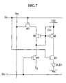
- FIGS. 3 , 5 , 7 , 8 and 10 are equivalent circuit diagrams of pixel circuits according to exemplary embodiments of the present invention.
- FIGS. 4 , 6 and 11 are driving waveform diagrams for driving the pixel circuits shown in FIGS. 3 , 5 and 10 , respectively;
- FIG. 9 is a diagram showing graphs that depict a current flowing to the organic EL element in the pixel circuit.
- FIG. 2 is a schematic diagram of the organic EL display device according to the exemplary embodiment of the present invention.
- the organic EL display device includes, as shown in FIG. 2 , an organic EL display panel 10 , a scan driver 20 , and a data driver 30 .
- the organic EL display panel 10 includes a plurality of data lines D 1 to D M arranged in columns, a plurality of scan lines S 1 to S N arranged in rows, and a plurality of pixel circuits 11 .
- the data lines D 1 to D M transfer a data voltage representing an image signal to the pixel circuits 11 .
- the scan lines S 1 to S N transfer a selection signals for selecting the pixel circuits 11 .
- Each of the pixel circuits 11 is formed in a pixel area defined by two adjacent data lines and two adjacent scan lines.
- the scan driver 20 sequentially applies the selection signal to the scan lines S 1 to S N , and the data driver 30 applies the data voltage representing an image signal to the data lines D 1 to D M .
- the scan driver 20 and/or the data driver 30 can be coupled to the display panel 10 , or mounted in the form of a chip on a tape carrier package (TCP) that is coupled to the display panel 10 by soldering.
- the scan driver 20 and/or the data driver 30 can also be mounted in the form of a chip on a flexible printed circuit (FPC) or a film coupled to the display panel by soldering. This method is called “CoF (Chip on Flexible board, or Chip on Film)”.
- the scan driver 20 and/or the data driver 30 can be mounted directly on the glass substrate of the display panel, or replaced for the driving circuit that includes is the same layers as scan and data lines and thin film transistors on the glass substrate. This method is called “CoG (Chip on Glass)”.
- the scan driver 20 and/or the data driver 30 may be mounted on any other suitable location using any suitable mounting method.
- FIG. 3 is an equivalent circuit diagram of the pixel circuit according to the exemplary embodiment of the present invention
- FIG. 4 is a driving waveform diagram for driving the pixel circuit shown in FIG. 3
- the pixel circuit is coupled to the m-th data line D m and the n-th scan line S n in FIG. 3 .
- the pixel circuit may be coupled to any other data line/scan line combination illustrated in FIG. 2 .
- the term “current scan line” as used herein refers to a scan line for transferring a current selection signal
- the term “previous scan line” as used herein refers to a scan line for transferring a selection signal prior to the current selection signal.
- the pixel circuit 11 includes, as shown in FIG. 3 , an organic EL element (OLED), transistors M 1 to M 5 , and a capacitor C st .
- the transistors M 1 to M 4 are PMOS type transistors, and the transistor M 5 is an NMOS type transistor.
- These transistors M 1 to M 5 should be thin film transistors, each of which has gate, drain and source electrodes formed on the glass substrate of the display panel 10 as a control electrode and two main electrodes, respectively.
- the driving transistor M 1 has a source electrode coupled to a power voltage V DD .
- a capacitor C st is coupled between the source electrode and a gate electrode.
- the capacitor C st sustains gate-source voltage V GS of the transistor M 1 for a period of time, which may be predefined.
- the compensating transistor M 2 is configured to operate as a diode (i.e., its gate and drain are coupled together).
- the gate of the compensating transistor M 2 is also coupled to the gate of the transistor M 1 .
- the switching transistor M 3 transfers, to the transistor M 2 , a data voltage from the data line D m in response to a selection signal from the current scan line S n .
- the drain of the transistor M 2 is coupled to the transistor M 4 .
- the transistor M 4 transfers a precharge voltage V P to the transistor M 2 in response to the selection signal from the previous scan line S n ⁇ 1 .
- the transistor M 5 is coupled between the drain of the transistor M 1 and the anode of the OLED, and electrically isolates the transistor M 1 from the OLED in response to the selection signal from the previous scan line S n ⁇ 1 .
- the OLED has a cathode coupled to a reference voltage V SS , and emits a light corresponding to the current applied.
- the reference voltage V SS is lower than the power voltage V DD and may be a ground voltage.
- the selection signal from the previous scan line S n ⁇ 1 becomes “low” to turn the transistor M 4 on and the transistor M 5 off.
- the precharge voltage V P is transferred to the gate of the transistor M 1 .
- the precharge voltage V P is slightly lower than any data voltage applied to the gate of the transistor M 1 through the transistor M 2 (taking into account the voltage drops in the transistors M 2 and M 4 , respectively), i.e., the lowest data voltage applied through the data line D m , for the sake of acquiring a maximum gradation level.
- the data voltage is always higher than the gate voltage of the transistor M 1 when it is applied through the data line D m . Therefore, the transistor M 1 is coupled in the forward direction so that the data voltage is charged in the capacitor C st .
- the gate-source voltage V GS of the transistor M 1 is increased due to the precharge voltage V P , so that a high current would flow through the transistor M 1 if a current path is available. If supplied to the OLED, this current would cause the OLED to emit a light, thereby preventing an accurate representation of a black level gradation.
- the turned-off transistor M 5 electrically isolates the transistor M 1 from the organic OLED to prevent a current flow, which otherwise would have been caused by the precharge voltage V P . This enables an accurate representation of black level gradation and prevents an unnecessary current flow, thereby also reducing power consumption.
- the selection signal from the previous scan line S n ⁇ 1 becomes “high” while the selection signal from the current scan line S n is sustained at a high level.
- the voltage on the data line D m is changed to a data voltage corresponding to the pixel circuit coupled to the current scan line S n .
- voltage on the data line D m should be saturated to a desired data voltage during the blanking time period T 2 .
- the previous data voltage applied to the data line D m may be transferred to the transistor M 1 via the transistor M 3 when the selection signal from the current scan line S n becomes “low” before the current data voltage is applied.
- the selection signal from the current scan line S n becomes “low” to turn the transistor M 3 on.
- the data voltage from the data line D m is transferred to the transistor M 2 through the transistor M 3 .
- the transistor M 2 is configured to operate as a diode, so the voltage corresponding to the data voltage minus threshold voltage V TH2 of the transistor M 2 is transferred to the gate of the transistor M 1 .
- This voltage is charged in the capacitor C st and sustained for a period of time, which may be predefined.
- the selection signal from the previous scan line S n ⁇ 1 becomes “high” to turn the transistor M 5 on. In practice, as indicated on FIG. 4 , the selection signal line S n ⁇ 1 from the previous scan line becomes “high” during the blanking time period T 2 , thereby turning on the transistor M 5 .
- a current I OLED corresponding to the gate-source voltage V GS of the transistor M 1 is supplied to the OLED, so the OLED emits a light.
- the current I OLED can be defined as follows.
- V TH1 is the threshold voltage of the transistor M 1
- V DATA is the data voltage from the data line D m
- ⁇ is a constant.
- I OLED ⁇ 2 ⁇ ( V DD - V DATA ) 2 [ Equation ⁇ ⁇ 2 ]
- the exemplary embodiment of the present invention compensates for a deviation of the threshold voltage of the driving transistor M 1 and prevents the current from flowing to the OLED caused by the precharge voltage V P .
- the pixel circuit according to the exemplary embodiment of the present invention uses the previous scan line S n ⁇ 1 so as to control the transistors M 4 and M 5 .
- a separate control line (not shown) may be used to transfer a control signal for turning the transistor M 4 on and/or the transistor M 5 off during the precharge time period T 1 .
- the type of the transistor M 5 is an opposite of that of the transistor M 4 so as to turn the transistor M 5 off during the precharge time period T 1 .
- the transistor M 5 may have the same type as the transistor M 4 in another embodiment of the present invention, which will be described, for example, in detail with reference to FIGS. 5 and 6 as follows.
- FIG. 5 is an equivalent circuit diagram of the pixel circuit according to another exemplary embodiment of the present invention
- FIG. 6 is a driving waveform diagram for driving the pixel circuit shown in FIG. 5 .
- the pixel circuit according to this exemplary embodiment of the present invention has the same structure as the exemplary embodiment of FIG. 3 except for the type of the transistor M 6 (which is different from the type of the transistor M 5 of FIG. 3 ) and an addition of a control line C n .
- the transistor M 6 is a PMOS type transistor, which is the same type as the transistors M 1 to M 4 , and turns off in response to a “high” control signal from the control line C n .
- the control signal applied to the control line C n is an inversed form of the selection signal applied to the previous scan line S n ⁇ 1 as shown in FIG. 6 .
- the transistor M 6 is turned off during the precharge time period T 1 to interrupt the current flowing to the OLED, as in the exemplary embodiment of FIG. 3 .
- this exemplary embodiment implements the pixel circuit with the transistors of the same type, thereby simplifying the fabrication process relative to the exemplary embodiment of FIG. 3 .
- the above described exemplary embodiments additionally use the transistors M 5 and M 6 , respectively, so as to interrupt the current flowing to the OLED during the precharge time period T 1 .
- a transistor may be added in addition to (or instead of) the transistor M 5 or M 6 , and the driving waveform may be selected so as to interrupt the current flowing to the OLED during the data charge time period T 3 .
- FIG. 7 One such exemplary embodiment will be described in detail with reference to FIG. 7 as follows.
- FIG. 7 is an equivalent circuit diagram of a pixel circuit according to yet another exemplary embodiment of the present invention.
- the pixel circuit according to this exemplary embodiment has a transistor M 5 coupled between the transistor M 1 and the OLED.
- the transistor M 5 is an NMOS type transistor similar to the transistor M 5 of FIG. 3 .
- the transistor M 5 has a gate coupled to the current scan line S n .
- the pixel circuit in this exemplary embodiment is driven by the driving waveform of FIG. 4 .
- the transistor M 5 is turned off in response to the selection signal from the current scan line S n to electrically isolate the transistor M 1 from the OLED while the data voltage from the data line D m is charged in the capacitor C st during the data charge time period T 3 .
- the current flowing to the OLED is interrupted while the data voltage is charged in the capacitor C st .
- the transistor M 5 As the selection signal from the current scan line S n becomes “high”, the transistor M 5 is turned on to couple the transistor M 1 to the OLED. Hence, a current I OLED corresponding to the voltage charged in the capacitor C st flows to the OLED, which then emits light in the light-emitting time period T 4 . Therefore, in this embodiment, the current flowing to the OLED is interrupted while the data voltage is charged, thereby reducing power consumption.
- the transistor M 5 may be of the same transistor type as the switching transistor M 3 .
- the transistor M 5 may be driven by a signal of an inversed form of the selection signal applied to the scan line S n to realize an equivalent pixel circuit as the pixel circuit of FIG. 7 .
- the current does not flow (i.e., is interrupted) to the OLED during the data charge time period T 3 .
- the current flowing to the OLED may also be interrupted during the precharge time period T 1 in other exemplary embodiments, one of which will be described in detail with reference to FIGS. 8 and 9 as follows.
- FIG. 8 is an equivalent circuit diagram of the pixel circuit according to still another exemplary embodiment of the present invention
- FIG. 9 shows a current flowing to the OLED in the pixel circuits shown in FIGS. 1 , 3 and 8 , respectively.
- the pixel circuit according to this exemplary embodiment has a transistor M 7 added to the pixel circuit in the exemplary embodiment of FIG. 3 .
- the transistors M 7 and M 5 are coupled in series between the transistor M 1 and the anode of the OLED, and formed with NMOS transistors.
- the gate of the transistor M 5 is coupled to the previous scan line S n ⁇ 1 , and that of the transistor M 7 is coupled to the current scan line S n .
- the transistors M 5 and M 7 can be switched in position.
- the pixel circuit of FIG. 8 is driven using the driving waveform of FIG. 4 .
- the transistor M 5 is turned off in response to the selection signal from the previous scan line S n ⁇ 1 during the precharge time period T 1 , so that no current flows to the OLED in response to the precharge voltage V P .
- the transistor M 7 is turned off in response to the selection signal from the current scan line S n during the data charge time period T 3 , so that no current flows to the OLED while the data voltage is charged.
- both the transistors M 5 and M 7 are turned on, and a current corresponding to the voltage charged in the capacitor C st flows to the OLED.
- the transistor M 5 may have the same transistor type as the transistor M 4 and applied with a signal having an inversed form of the selection signal applied to the previous scan line S n ⁇ 1 to the gate of the transistor M 5 .
- the transistor M 7 may be formed to have the same transistor type as the transistor M 3 , and applied with a signal having an inversed form of the selection signal applied to the current scan line S n . The operation of such pixel circuits would be equivalent to that of the pixel circuit of FIG. 8 .
- the pixel circuit of FIG. 1 allows a current to flow to the OLED during both the precharge time period T 1 and the data charge time period T 3 .
- the pixel circuit of FIG. 3 allows a current to flow to the OLED not in the precharge time period T 1 but in the data charge time period T 3 .
- the pixel circuit of FIG. 8 does not allow a current to flow to OLED during both the precharge time period T 1 and the data charge time period T 3 .
- the transistors M 1 to M 4 are formed with PMOS type transistors in the above described exemplary embodiments, they may also be formed with NMOS type transistors in other embodiments. One such exemplary embodiment will be described in detail with reference to FIGS. 10 and 11 . In still other embodiments, the transistors M 1 to M 4 may be any other suitable transistors.
- FIG. 10 is an equivalent circuit diagram of the pixel circuit according to a still further exemplary embodiment of the present invention
- FIG. 11 is a driving waveform diagram for the pixel circuit shown in FIG. 10 .
- the pixel circuit according to this embodiment has transistors M 11 to M 14 formed with NMOS type transistors, and transistors M 15 and M 16 formed with PMOS type transistors.
- the pixel circuit of FIG. 10 also has a structure that is symmetrical to the pixel circuit of FIG. 8 . More specifically, the transistor M 11 has a source electrode coupled to the reference voltage V SS , and the OLED has an anode coupled to the power voltage V DD .
- the transistors M 15 and M 16 are coupled in series between the cathode of the OLED and the drain of the transistor M 11 .
- the driving waveform for the pixel circuit of FIG. 10 has an inverted form of the driving waveform (in FIG. 4 ) of the pixel circuit of FIG. 8 .
- the pixel circuit of FIG. 10 performs an equivalent operation as the pixel circuit of FIG. 8 , and its operation will not be described in detail.
- the transistors M 11 to M 14 formed with NMOS type transistors can be applied to all the embodiments of the present invention. Likewise, if the same functions of the above-stated transistors are enabled, the pixel circuit can be implemented with a combination of PMOS and NMOS transistors or other switching elements.
- the exemplary embodiments according to the present invention may compensate for a deviation of the threshold voltage of the transistors when the driving transistor has the same threshold voltage as the compensating transistor.
- a current may not be provided to the OLED while the precharge voltage is being charged in a capacitor, thereby allowing an accurate representation of black level gradation, which may enhance a contrast ratio. Further, a current may not be provided to the OLED while the data voltage is being charged, thereby reducing power consumption.
- the present invention is not specifically limited to the organic EL display device and may be applied to other light-emitting display devices that emit a light in response to the current applied.
Landscapes
- Engineering & Computer Science (AREA)
- Physics & Mathematics (AREA)
- Computer Hardware Design (AREA)
- General Physics & Mathematics (AREA)
- Theoretical Computer Science (AREA)
- Control Of Indicators Other Than Cathode Ray Tubes (AREA)
- Control Of El Displays (AREA)
- Electroluminescent Light Sources (AREA)
- Shift Register Type Memory (AREA)
Applications Claiming Priority (3)
| Application Number | Priority Date | Filing Date | Title |
|---|---|---|---|
| KR10-2003-0027604A KR100515299B1 (ko) | 2003-04-30 | 2003-04-30 | 화상 표시 장치와 그 표시 패널 및 구동 방법 |
| KR10-2003-0027604 | 2003-04-30 | ||
| KR2003-27604 | 2003-04-30 |
Publications (2)
| Publication Number | Publication Date |
|---|---|
| US20040217925A1 US20040217925A1 (en) | 2004-11-04 |
| US7403176B2 true US7403176B2 (en) | 2008-07-22 |
Family
ID=32985940
Family Applications (1)
| Application Number | Title | Priority Date | Filing Date |
|---|---|---|---|
| US10/634,337 Expired - Fee Related US7403176B2 (en) | 2003-04-30 | 2003-08-04 | Image display device, and display panel and driving method thereof, and pixel circuit |
Country Status (6)
| Country | Link |
|---|---|
| US (1) | US7403176B2 (de) |
| EP (1) | EP1473689B1 (de) |
| JP (1) | JP2004334163A (de) |
| KR (1) | KR100515299B1 (de) |
| CN (1) | CN100399392C (de) |
| DE (1) | DE60324097D1 (de) |
Cited By (15)
| Publication number | Priority date | Publication date | Assignee | Title |
|---|---|---|---|---|
| US20050110727A1 (en) * | 2003-11-26 | 2005-05-26 | Dong-Yong Shin | Demultiplexing device and display device using the same |
| US20050116919A1 (en) * | 2003-11-27 | 2005-06-02 | Dong-Yong Shin | Display device using demultiplexer and driving method thereof |
| US20050117611A1 (en) * | 2003-11-27 | 2005-06-02 | Dong-Yong Shin | Display device using demultiplexer |
| US20050140666A1 (en) * | 2003-11-27 | 2005-06-30 | Dong-Yong Shin | Display device using demultiplexer and driving method thereof |
| US20050259052A1 (en) * | 2004-05-15 | 2005-11-24 | Dong-Yong Shin | Display device and demultiplexer |
| US20050264495A1 (en) * | 2004-05-25 | 2005-12-01 | Dong-Yong Shin | Display device and demultiplexer |
| US20060022909A1 (en) * | 2004-07-28 | 2006-02-02 | Won-Kyu Kwak | Light emitting display (LED) and display panel and pixel circuit thereof |
| US20070018917A1 (en) * | 2005-07-15 | 2007-01-25 | Seiko Epson Corporation | Electronic device, method of driving the same, electro-optical device, and electronic apparatus |
| US20070205964A1 (en) * | 2004-04-12 | 2007-09-06 | Matsushita Electric Industrial Co., Ltd. | Plasma display panel display device |
| US20070273618A1 (en) * | 2006-05-26 | 2007-11-29 | Toppoly Optoelectronics Corp. | Pixels and display panels |
| US20070279343A1 (en) * | 2006-06-05 | 2007-12-06 | Samsung Sdi Co., Ltd. | Organic electroluminescence display and driving method thereof |
| US20110227815A1 (en) * | 2010-03-19 | 2011-09-22 | Dialog Semiconductor Gmbh | PWM precharge of organic light emitting diodes |
| US20110234648A1 (en) * | 2010-03-23 | 2011-09-29 | Hitachi Displays, Ltd. | Display device |
| US8269803B2 (en) | 2010-04-14 | 2012-09-18 | Samsung Mobile Display Co., Ltd. | Display device and method for driving the same |
| TWI427593B (zh) * | 2009-10-21 | 2014-02-21 | Chi Mei El Corp | 有機發光二極體顯示模組、有機發光二極體顯示裝置及其影像補償方法 |
Families Citing this family (87)
| Publication number | Priority date | Publication date | Assignee | Title |
|---|---|---|---|---|
| KR100939206B1 (ko) * | 2003-06-27 | 2010-01-28 | 엘지디스플레이 주식회사 | 일렉트로-루미네센스 표시장치 및 그 구동방법 |
| KR100560468B1 (ko) * | 2003-09-16 | 2006-03-13 | 삼성에스디아이 주식회사 | 화상 표시 장치와 그 표시 패널 |
| KR100778409B1 (ko) * | 2003-10-29 | 2007-11-22 | 삼성에스디아이 주식회사 | 화상 표시 패널 및 그 구동 방법 |
| KR100515306B1 (ko) | 2003-10-29 | 2005-09-15 | 삼성에스디아이 주식회사 | 유기el 표시패널 |
| KR20050041665A (ko) * | 2003-10-31 | 2005-05-04 | 삼성에스디아이 주식회사 | 화상 표시 장치 및 그 구동 방법 |
| KR100529077B1 (ko) * | 2003-11-13 | 2005-11-15 | 삼성에스디아이 주식회사 | 화상 표시 장치, 그 표시 패널 및 그 구동 방법 |
| KR100578793B1 (ko) * | 2003-11-26 | 2006-05-11 | 삼성에스디아이 주식회사 | 발광 표시 장치 및 그 구동 방법 |
| JP4147410B2 (ja) * | 2003-12-02 | 2008-09-10 | ソニー株式会社 | トランジスタ回路、画素回路、表示装置及びこれらの駆動方法 |
| JP4107240B2 (ja) * | 2004-01-21 | 2008-06-25 | セイコーエプソン株式会社 | 駆動回路、電気光学装置及び電気光学装置の駆動方法、並びに電子機器 |
| KR100560479B1 (ko) * | 2004-03-10 | 2006-03-13 | 삼성에스디아이 주식회사 | 발광 표시 장치 및 그 표시 패널과 구동 방법 |
| KR100560444B1 (ko) * | 2004-03-24 | 2006-03-13 | 삼성에스디아이 주식회사 | 발광 표시 장치 및 그 구동방법 |
| KR100792467B1 (ko) * | 2004-04-16 | 2008-01-08 | 엘지.필립스 엘시디 주식회사 | 디지털 구동을 위한 유기전계 발광 디스플레이 장치 및이의 구동방법 |
| US8378930B2 (en) * | 2004-05-28 | 2013-02-19 | Sony Corporation | Pixel circuit and display device having symmetric pixel circuits and shared voltage lines |
| JP5105699B2 (ja) * | 2004-06-18 | 2012-12-26 | 三菱電機株式会社 | 表示装置 |
| KR101080351B1 (ko) | 2004-06-22 | 2011-11-04 | 삼성전자주식회사 | 표시 장치 및 그 구동 방법 |
| JP4834876B2 (ja) * | 2004-06-25 | 2011-12-14 | 京セラ株式会社 | 画像表示装置 |
| KR100698681B1 (ko) * | 2004-06-29 | 2007-03-23 | 삼성에스디아이 주식회사 | 발광 표시장치 |
| KR100590066B1 (ko) | 2004-07-28 | 2006-06-14 | 삼성에스디아이 주식회사 | 발광 표시 장치 및 그 표시 패널 |
| KR101087417B1 (ko) * | 2004-08-13 | 2011-11-25 | 엘지디스플레이 주식회사 | 유기 발광표시장치의 구동회로 |
| KR100662978B1 (ko) * | 2004-08-25 | 2006-12-28 | 삼성에스디아이 주식회사 | 발광 표시장치와 그의 구동방법 |
| US20060077138A1 (en) * | 2004-09-15 | 2006-04-13 | Kim Hong K | Organic light emitting display and driving method thereof |
| EP2383721B1 (de) | 2004-11-16 | 2015-04-08 | Ignis Innovation Inc. | System und Ansteuerungsverfahren der Anzeige einer lichtemittierenden Aktivmatrix-Vorrichtung |
| KR100600344B1 (ko) * | 2004-11-22 | 2006-07-18 | 삼성에스디아이 주식회사 | 화소회로 및 발광 표시장치 |
| CA2490858A1 (en) | 2004-12-07 | 2006-06-07 | Ignis Innovation Inc. | Driving method for compensated voltage-programming of amoled displays |
| KR100604066B1 (ko) | 2004-12-24 | 2006-07-24 | 삼성에스디아이 주식회사 | 화소 및 이를 이용한 발광 표시장치 |
| CN100430985C (zh) * | 2004-12-29 | 2008-11-05 | 普诚科技股份有限公司 | 有机发光二极管面板的二段式驱动电路 |
| KR100602363B1 (ko) | 2005-01-10 | 2006-07-18 | 삼성에스디아이 주식회사 | 발광제어구동부 및 그를 이용한 발광 표시장치 |
| KR101152119B1 (ko) * | 2005-02-07 | 2012-06-15 | 삼성전자주식회사 | 표시 장치 및 그 구동 방법 |
| KR101152120B1 (ko) | 2005-03-16 | 2012-06-15 | 삼성전자주식회사 | 표시 장치 및 그 구동 방법 |
| KR100719924B1 (ko) | 2005-04-29 | 2007-05-18 | 비오이 하이디스 테크놀로지 주식회사 | 유기 전계발광 표시장치 |
| KR100782455B1 (ko) * | 2005-04-29 | 2007-12-05 | 삼성에스디아이 주식회사 | 발광제어 구동장치 및 이를 구비하는 유기전계발광표시장치 |
| US7852298B2 (en) | 2005-06-08 | 2010-12-14 | Ignis Innovation Inc. | Method and system for driving a light emitting device display |
| JP4983018B2 (ja) * | 2005-12-26 | 2012-07-25 | ソニー株式会社 | 表示装置及びその駆動方法 |
| US9269322B2 (en) | 2006-01-09 | 2016-02-23 | Ignis Innovation Inc. | Method and system for driving an active matrix display circuit |
| US9489891B2 (en) | 2006-01-09 | 2016-11-08 | Ignis Innovation Inc. | Method and system for driving an active matrix display circuit |
| TWI338874B (en) * | 2006-03-10 | 2011-03-11 | Au Optronics Corp | Light emitting diode display and driving pixel method thereof |
| CN100412935C (zh) * | 2006-05-18 | 2008-08-20 | 友达光电股份有限公司 | 有机电致发光显示器的驱动电路与驱动方法 |
| JP4203770B2 (ja) | 2006-05-29 | 2009-01-07 | ソニー株式会社 | 画像表示装置 |
| JP2007316453A (ja) * | 2006-05-29 | 2007-12-06 | Sony Corp | 画像表示装置 |
| JP2007316454A (ja) | 2006-05-29 | 2007-12-06 | Sony Corp | 画像表示装置 |
| JP2007323036A (ja) * | 2006-06-05 | 2007-12-13 | Samsung Sdi Co Ltd | 有機電界発光表示装置及びその駆動方法 |
| KR20080000294A (ko) * | 2006-06-27 | 2008-01-02 | 엘지.필립스 엘시디 주식회사 | 유기전계 발광 디스플레이 장치 및 그 구동방법 |
| CN101281916B (zh) * | 2007-04-06 | 2010-05-26 | 群康科技(深圳)有限公司 | 光感测器和显示装置 |
| KR20100134125A (ko) | 2008-04-18 | 2010-12-22 | 이그니스 이노베이션 인크. | 발광 소자 디스플레이에 대한 시스템 및 구동 방법 |
| US8207918B2 (en) * | 2008-06-11 | 2012-06-26 | Hitachi Displays, Ltd. | Image display device having a set period during which a step signal is supplied at different levels to provide a uniform display |
| CA2637343A1 (en) | 2008-07-29 | 2010-01-29 | Ignis Innovation Inc. | Improving the display source driver |
| JP5384051B2 (ja) * | 2008-08-27 | 2014-01-08 | 株式会社ジャパンディスプレイ | 画像表示装置 |
| US9370075B2 (en) | 2008-12-09 | 2016-06-14 | Ignis Innovation Inc. | System and method for fast compensation programming of pixels in a display |
| KR101030004B1 (ko) * | 2009-09-30 | 2011-04-20 | 삼성모바일디스플레이주식회사 | 화소 회로 및 이를 이용한 유기전계발광 표시 장치 |
| CN101702847B (zh) * | 2009-11-13 | 2014-04-09 | 无锡灿星科技有限公司 | 不随温度、工艺变化的无过冲快速预充电电路 |
| CN102376282B (zh) * | 2010-08-25 | 2013-05-01 | 中国科学院微电子研究所 | 一种硅基液晶显示器件的场缓存像素电路 |
| US9886899B2 (en) | 2011-05-17 | 2018-02-06 | Ignis Innovation Inc. | Pixel Circuits for AMOLED displays |
| US9351368B2 (en) | 2013-03-08 | 2016-05-24 | Ignis Innovation Inc. | Pixel circuits for AMOLED displays |
| US20140368491A1 (en) | 2013-03-08 | 2014-12-18 | Ignis Innovation Inc. | Pixel circuits for amoled displays |
| EP2715711A4 (de) | 2011-05-28 | 2014-12-24 | Ignis Innovation Inc | System und verfahren zur schnellen kompensationsprogrammierung von pixeln auf einer anzeige |
| US9747834B2 (en) | 2012-05-11 | 2017-08-29 | Ignis Innovation Inc. | Pixel circuits including feedback capacitors and reset capacitors, and display systems therefore |
| KR101911489B1 (ko) * | 2012-05-29 | 2018-10-26 | 삼성디스플레이 주식회사 | 화소를 갖는 유기전계발광 표시장치와 그의 구동방법 |
| CN102820006B (zh) * | 2012-08-02 | 2015-10-14 | 京东方科技集团股份有限公司 | 一种补偿阈值电压漂移的像素电路和薄膜晶体管背板 |
| US9336717B2 (en) | 2012-12-11 | 2016-05-10 | Ignis Innovation Inc. | Pixel circuits for AMOLED displays |
| US9786223B2 (en) | 2012-12-11 | 2017-10-10 | Ignis Innovation Inc. | Pixel circuits for AMOLED displays |
| CN103021339B (zh) | 2012-12-31 | 2015-09-16 | 昆山工研院新型平板显示技术中心有限公司 | 像素电路、显示装置及其驱动方法 |
| KR102055622B1 (ko) * | 2013-01-10 | 2020-01-23 | 삼성디스플레이 주식회사 | 평판 표시 장치 및 평판 표시 장치의 구동 방법 |
| CA2894717A1 (en) | 2015-06-19 | 2016-12-19 | Ignis Innovation Inc. | Optoelectronic device characterization in array with shared sense line |
| US9721505B2 (en) | 2013-03-08 | 2017-08-01 | Ignis Innovation Inc. | Pixel circuits for AMOLED displays |
| CN104464612A (zh) * | 2013-09-22 | 2015-03-25 | 昆山工研院新型平板显示技术中心有限公司 | 像素电路及使用该像素电路的有机发光显示器 |
| US9406705B2 (en) * | 2014-02-25 | 2016-08-02 | Lg Display Co., Ltd. | Display backplane having multiple types of thin-film-transistors |
| US20150348473A1 (en) * | 2014-05-30 | 2015-12-03 | Qualcomm Mems Technologies, Inc. | Systems, devices, and methods for driving an analog interferometric modulator utilizing dc common with reset |
| CA2873476A1 (en) | 2014-12-08 | 2016-06-08 | Ignis Innovation Inc. | Smart-pixel display architecture |
| CN104575395B (zh) * | 2015-02-03 | 2017-10-13 | 深圳市华星光电技术有限公司 | Amoled像素驱动电路 |
| CN104637445B (zh) * | 2015-02-03 | 2017-03-08 | 深圳市华星光电技术有限公司 | Amoled像素驱动电路及像素驱动方法 |
| CA2886862A1 (en) | 2015-04-01 | 2016-10-01 | Ignis Innovation Inc. | Adjusting display brightness for avoiding overheating and/or accelerated aging |
| CN104867456B (zh) * | 2015-06-19 | 2017-12-22 | 合肥鑫晟光电科技有限公司 | 像素电路及其驱动方法、显示装置 |
| US10373554B2 (en) | 2015-07-24 | 2019-08-06 | Ignis Innovation Inc. | Pixels and reference circuits and timing techniques |
| CA2898282A1 (en) | 2015-07-24 | 2017-01-24 | Ignis Innovation Inc. | Hybrid calibration of current sources for current biased voltage progra mmed (cbvp) displays |
| US10657895B2 (en) | 2015-07-24 | 2020-05-19 | Ignis Innovation Inc. | Pixels and reference circuits and timing techniques |
| CA2908285A1 (en) | 2015-10-14 | 2017-04-14 | Ignis Innovation Inc. | Driver with multiple color pixel structure |
| EP3389039A1 (de) | 2017-04-13 | 2018-10-17 | Samsung Electronics Co., Ltd. | Anzeigetafel und verfahren zur ansteuerung einer anzeigetafel |
| CN107068045A (zh) * | 2017-05-23 | 2017-08-18 | 上海和辉光电有限公司 | 一种像素电路、驱动方法及显示器 |
| CN107230448A (zh) * | 2017-05-23 | 2017-10-03 | 上海和辉光电有限公司 | 一种像素电路、驱动方法及显示器 |
| KR102344964B1 (ko) * | 2017-08-09 | 2021-12-29 | 엘지디스플레이 주식회사 | 표시장치, 전자기기 및 바디 바이어싱 회로 |
| US11004397B2 (en) * | 2017-09-21 | 2021-05-11 | Sharp Kabushiki Kaisha | Display device and method for driving same |
| CN110459167B (zh) * | 2018-05-08 | 2021-01-26 | 京东方科技集团股份有限公司 | 像素电路及其驱动方法和显示装置 |
| KR102632905B1 (ko) * | 2018-07-18 | 2024-02-06 | 삼성디스플레이 주식회사 | 유기 발광 표시 장치 및 이의 구동 방법 |
| CN109741708A (zh) * | 2019-02-26 | 2019-05-10 | 深圳市华星光电半导体显示技术有限公司 | 像素驱动电路及显示面板 |
| CN112750392B (zh) * | 2019-10-30 | 2022-04-15 | 京东方科技集团股份有限公司 | 像素驱动电路及其驱动方法、显示面板、显示装置 |
| US11996035B2 (en) | 2021-03-11 | 2024-05-28 | Boe Technology Group Co., Ltd. | Pixel circuit and method for driving same, display panel, and display device |
| CN116129810B (zh) | 2023-02-14 | 2024-07-23 | 武汉天马微电子有限公司 | 显示面板及显示装置 |
Citations (31)
| Publication number | Priority date | Publication date | Assignee | Title |
|---|---|---|---|---|
| US4595919A (en) | 1983-08-22 | 1986-06-17 | Burroughs Corporation | System and method for operating a display panel having memory |
| JPH0282295A (ja) | 1988-09-20 | 1990-03-22 | Fujitsu Ltd | マトリクス表示装置のデータドライバ |
| JPH06332397A (ja) | 1993-05-25 | 1994-12-02 | Fujitsu Ltd | フラットパネルディスプレイ装置 |
| US5426447A (en) | 1992-11-04 | 1995-06-20 | Yuen Foong Yu H.K. Co., Ltd. | Data driving circuit for LCD display |
| US5510807A (en) | 1993-01-05 | 1996-04-23 | Yuen Foong Yu H.K. Co., Ltd. | Data driver circuit and associated method for use with scanned LCD video display |
| US5686936A (en) | 1994-04-22 | 1997-11-11 | Sony Corporation | Active matrix display device and method therefor |
| US5708454A (en) | 1993-05-31 | 1998-01-13 | Sharp Kabushiki Kaisha | Matrix type display apparatus and a method for driving the same |
| US5835072A (en) | 1995-09-13 | 1998-11-10 | Fujitsu Limited | Driving method for plasma display permitting improved gray-scale display, and plasma display |
| EP0905673A1 (de) | 1997-09-29 | 1999-03-31 | Sarnoff Corporation | Anzeigesystem mit aktiver Matrix und Steuerverfahren dafür |
| JPH11272233A (ja) | 1998-03-18 | 1999-10-08 | Seiko Epson Corp | トランジスタ回路、表示パネル及び電子機器 |
| WO2001006484A1 (en) | 1999-07-14 | 2001-01-25 | Sony Corporation | Current drive circuit and display comprising the same, pixel circuit, and drive method |
| US6229506B1 (en) * | 1997-04-23 | 2001-05-08 | Sarnoff Corporation | Active matrix light emitting diode pixel structure and concomitant method |
| US6369786B1 (en) * | 1998-04-30 | 2002-04-09 | Sony Corporation | Matrix driving method and apparatus for current-driven display elements |
| US20020047581A1 (en) * | 2000-10-24 | 2002-04-25 | Jun Koyama | Light emitting device and method of driving the same |
| EP1220191A2 (de) | 2000-12-29 | 2002-07-03 | Samsung SDI Co., Ltd. | Organische elektrolumineszierende Anzeigevorrichtung, Ansteuerverfahren und Pixelschaltung |
| US6469318B2 (en) | 2000-09-29 | 2002-10-22 | Sanyo Electric Co., Ltd. | Semiconductor device having thin film transistor for supplying current to driven element |
| JP2002351401A (ja) | 2001-03-21 | 2002-12-06 | Mitsubishi Electric Corp | 自発光型表示装置 |
| US6501448B1 (en) | 1999-01-29 | 2002-12-31 | Sanyo Electric Co., Ltd. | Electroluminescence display device with improved driving transistor structure |
| US6518943B1 (en) | 1999-06-01 | 2003-02-11 | Pioneer Corporation | Driving apparatus for driving a plasma display panel |
| US6580408B1 (en) | 1999-06-03 | 2003-06-17 | Lg. Philips Lcd Co., Ltd. | Electro-luminescent display including a current mirror |
| US20030179162A1 (en) | 2002-03-20 | 2003-09-25 | Fujitsu Hitachi Plasma Display Limited | Display apparatus capable of maintaining high image quality without dependence on display load, and method for driving the same |
| US20030179164A1 (en) | 2002-03-21 | 2003-09-25 | Dong-Yong Shin | Display and a driving method thereof |
| US6650060B2 (en) * | 2001-01-22 | 2003-11-18 | Pioneer Corporation | Pixel driving circuit for light emitting display |
| US20040041769A1 (en) | 2001-10-17 | 2004-03-04 | Junichi Yamashita | Display apparatus |
| JP2004118196A (ja) | 2002-09-25 | 2004-04-15 | Samsung Electronics Co Ltd | 有機電界発光駆動素子とこれを有する有機電界発光表示パネル |
| US6731266B1 (en) | 1998-09-03 | 2004-05-04 | Samsung Electronics Co., Ltd. | Driving device and driving method for a display device |
| US6760005B2 (en) * | 2000-07-25 | 2004-07-06 | Semiconductor Energy Laboratory Co., Ltd. | Driver circuit of a display device |
| US6791129B2 (en) | 2000-04-27 | 2004-09-14 | Semiconductor Energy Laboratory Co., Ltd. | Light emitting device |
| US6809482B2 (en) * | 2001-06-01 | 2004-10-26 | Semiconductor Energy Laboratory Co., Ltd. | Light emitting device and method of driving the same |
| US6989826B2 (en) * | 2001-08-02 | 2006-01-24 | Seiko Epson Corporation | Driving of data lines used in unit circuit control |
| US7209101B2 (en) * | 2001-08-29 | 2007-04-24 | Nec Corporation | Current load device and method for driving the same |
Family Cites Families (1)
| Publication number | Priority date | Publication date | Assignee | Title |
|---|---|---|---|---|
| US8823606B2 (en) * | 2001-09-07 | 2014-09-02 | Panasonic Corporation | EL display panel, its driving method, and EL display apparatus |
-
2003
- 2003-04-30 KR KR10-2003-0027604A patent/KR100515299B1/ko not_active Expired - Fee Related
- 2003-08-04 US US10/634,337 patent/US7403176B2/en not_active Expired - Fee Related
- 2003-08-21 EP EP03090266A patent/EP1473689B1/de not_active Expired - Lifetime
- 2003-08-21 DE DE60324097T patent/DE60324097D1/de not_active Expired - Lifetime
- 2003-08-28 CN CNB031555462A patent/CN100399392C/zh not_active Expired - Fee Related
- 2003-09-29 JP JP2003337939A patent/JP2004334163A/ja active Pending
Patent Citations (37)
| Publication number | Priority date | Publication date | Assignee | Title |
|---|---|---|---|---|
| US4595919A (en) | 1983-08-22 | 1986-06-17 | Burroughs Corporation | System and method for operating a display panel having memory |
| JPH0282295A (ja) | 1988-09-20 | 1990-03-22 | Fujitsu Ltd | マトリクス表示装置のデータドライバ |
| US5426447A (en) | 1992-11-04 | 1995-06-20 | Yuen Foong Yu H.K. Co., Ltd. | Data driving circuit for LCD display |
| US5510807A (en) | 1993-01-05 | 1996-04-23 | Yuen Foong Yu H.K. Co., Ltd. | Data driver circuit and associated method for use with scanned LCD video display |
| JPH06332397A (ja) | 1993-05-25 | 1994-12-02 | Fujitsu Ltd | フラットパネルディスプレイ装置 |
| US5708454A (en) | 1993-05-31 | 1998-01-13 | Sharp Kabushiki Kaisha | Matrix type display apparatus and a method for driving the same |
| US5686936A (en) | 1994-04-22 | 1997-11-11 | Sony Corporation | Active matrix display device and method therefor |
| US5835072A (en) | 1995-09-13 | 1998-11-10 | Fujitsu Limited | Driving method for plasma display permitting improved gray-scale display, and plasma display |
| US6229506B1 (en) * | 1997-04-23 | 2001-05-08 | Sarnoff Corporation | Active matrix light emitting diode pixel structure and concomitant method |
| EP0905673A1 (de) | 1997-09-29 | 1999-03-31 | Sarnoff Corporation | Anzeigesystem mit aktiver Matrix und Steuerverfahren dafür |
| US6229508B1 (en) * | 1997-09-29 | 2001-05-08 | Sarnoff Corporation | Active matrix light emitting diode pixel structure and concomitant method |
| JPH11272233A (ja) | 1998-03-18 | 1999-10-08 | Seiko Epson Corp | トランジスタ回路、表示パネル及び電子機器 |
| US6362798B1 (en) | 1998-03-18 | 2002-03-26 | Seiko Epson Corporation | Transistor circuit, display panel and electronic apparatus |
| US6369786B1 (en) * | 1998-04-30 | 2002-04-09 | Sony Corporation | Matrix driving method and apparatus for current-driven display elements |
| US6731266B1 (en) | 1998-09-03 | 2004-05-04 | Samsung Electronics Co., Ltd. | Driving device and driving method for a display device |
| US6501448B1 (en) | 1999-01-29 | 2002-12-31 | Sanyo Electric Co., Ltd. | Electroluminescence display device with improved driving transistor structure |
| US6518943B1 (en) | 1999-06-01 | 2003-02-11 | Pioneer Corporation | Driving apparatus for driving a plasma display panel |
| US6580408B1 (en) | 1999-06-03 | 2003-06-17 | Lg. Philips Lcd Co., Ltd. | Electro-luminescent display including a current mirror |
| WO2001006484A1 (en) | 1999-07-14 | 2001-01-25 | Sony Corporation | Current drive circuit and display comprising the same, pixel circuit, and drive method |
| US6791129B2 (en) | 2000-04-27 | 2004-09-14 | Semiconductor Energy Laboratory Co., Ltd. | Light emitting device |
| US6760005B2 (en) * | 2000-07-25 | 2004-07-06 | Semiconductor Energy Laboratory Co., Ltd. | Driver circuit of a display device |
| US6469318B2 (en) | 2000-09-29 | 2002-10-22 | Sanyo Electric Co., Ltd. | Semiconductor device having thin film transistor for supplying current to driven element |
| US20020047581A1 (en) * | 2000-10-24 | 2002-04-25 | Jun Koyama | Light emitting device and method of driving the same |
| US20020118150A1 (en) | 2000-12-29 | 2002-08-29 | Oh-Kyong Kwon | Organic electroluminescent display, driving method and pixel circuit thereof |
| EP1220191A3 (de) | 2000-12-29 | 2003-09-10 | Samsung SDI Co., Ltd. | Organische elektrolumineszierende Anzeigevorrichtung, Ansteuerverfahren und Pixelschaltung |
| US7015884B2 (en) | 2000-12-29 | 2006-03-21 | Samsung Sdi Co., Ltd. | Organic electroluminescent display, driving method and pixel circuit thereof |
| EP1220191A2 (de) | 2000-12-29 | 2002-07-03 | Samsung SDI Co., Ltd. | Organische elektrolumineszierende Anzeigevorrichtung, Ansteuerverfahren und Pixelschaltung |
| CN1361510A (zh) | 2000-12-29 | 2002-07-31 | 三星Sdi株式会社 | 有机电发光显示器及其驱动方法和像素电路 |
| US6650060B2 (en) * | 2001-01-22 | 2003-11-18 | Pioneer Corporation | Pixel driving circuit for light emitting display |
| JP2002351401A (ja) | 2001-03-21 | 2002-12-06 | Mitsubishi Electric Corp | 自発光型表示装置 |
| US6809482B2 (en) * | 2001-06-01 | 2004-10-26 | Semiconductor Energy Laboratory Co., Ltd. | Light emitting device and method of driving the same |
| US6989826B2 (en) * | 2001-08-02 | 2006-01-24 | Seiko Epson Corporation | Driving of data lines used in unit circuit control |
| US7209101B2 (en) * | 2001-08-29 | 2007-04-24 | Nec Corporation | Current load device and method for driving the same |
| US20040041769A1 (en) | 2001-10-17 | 2004-03-04 | Junichi Yamashita | Display apparatus |
| US20030179162A1 (en) | 2002-03-20 | 2003-09-25 | Fujitsu Hitachi Plasma Display Limited | Display apparatus capable of maintaining high image quality without dependence on display load, and method for driving the same |
| US20030179164A1 (en) | 2002-03-21 | 2003-09-25 | Dong-Yong Shin | Display and a driving method thereof |
| JP2004118196A (ja) | 2002-09-25 | 2004-04-15 | Samsung Electronics Co Ltd | 有機電界発光駆動素子とこれを有する有機電界発光表示パネル |
Non-Patent Citations (2)
| Title |
|---|
| European Search Report for Application No. EP 03 00 6113; Jan. 18, 2004; 2 pages. |
| Patents Abstracts of Japan, Publication No. JP11-272233, Published on Oct. 8, 1999 in the name of Kimura. |
Cited By (25)
| Publication number | Priority date | Publication date | Assignee | Title |
|---|---|---|---|---|
| US20050110727A1 (en) * | 2003-11-26 | 2005-05-26 | Dong-Yong Shin | Demultiplexing device and display device using the same |
| US7728806B2 (en) | 2003-11-26 | 2010-06-01 | Samsung Mobile Display Co., Ltd. | Demultiplexing device and display device using the same |
| US20050140666A1 (en) * | 2003-11-27 | 2005-06-30 | Dong-Yong Shin | Display device using demultiplexer and driving method thereof |
| US20050117611A1 (en) * | 2003-11-27 | 2005-06-02 | Dong-Yong Shin | Display device using demultiplexer |
| US7738512B2 (en) | 2003-11-27 | 2010-06-15 | Samsung Mobile Display Co., Ltd. | Display device using demultiplexer |
| US20050116919A1 (en) * | 2003-11-27 | 2005-06-02 | Dong-Yong Shin | Display device using demultiplexer and driving method thereof |
| US7728827B2 (en) | 2003-11-27 | 2010-06-01 | Samsung Mobile Display Co., Ltd. | Display device using demultiplexer and driving method thereof |
| US7619602B2 (en) * | 2003-11-27 | 2009-11-17 | Samsung Mobile Display Co., Ltd. | Display device using demultiplexer and driving method thereof |
| US20070205964A1 (en) * | 2004-04-12 | 2007-09-06 | Matsushita Electric Industrial Co., Ltd. | Plasma display panel display device |
| US7692673B2 (en) | 2004-05-15 | 2010-04-06 | Samsung Mobile Display Co., Ltd. | Display device and demultiplexer |
| US20050259052A1 (en) * | 2004-05-15 | 2005-11-24 | Dong-Yong Shin | Display device and demultiplexer |
| US20050264495A1 (en) * | 2004-05-25 | 2005-12-01 | Dong-Yong Shin | Display device and demultiplexer |
| US7782277B2 (en) | 2004-05-25 | 2010-08-24 | Samsung Mobile Display Co., Ltd. | Display device having demultiplexer |
| US20060022909A1 (en) * | 2004-07-28 | 2006-02-02 | Won-Kyu Kwak | Light emitting display (LED) and display panel and pixel circuit thereof |
| US7545352B2 (en) * | 2004-07-28 | 2009-06-09 | Samsung Mobile Display Co., Ltd. | Light emitting display (LED) and display panel and pixel circuit thereof |
| US20070018917A1 (en) * | 2005-07-15 | 2007-01-25 | Seiko Epson Corporation | Electronic device, method of driving the same, electro-optical device, and electronic apparatus |
| US20070273618A1 (en) * | 2006-05-26 | 2007-11-29 | Toppoly Optoelectronics Corp. | Pixels and display panels |
| US20070279343A1 (en) * | 2006-06-05 | 2007-12-06 | Samsung Sdi Co., Ltd. | Organic electroluminescence display and driving method thereof |
| US7847768B2 (en) | 2006-06-05 | 2010-12-07 | Samsung Mobile Display Co., Ltd. | Organic electroluminescence display and driving method thereof |
| TWI427593B (zh) * | 2009-10-21 | 2014-02-21 | Chi Mei El Corp | 有機發光二極體顯示模組、有機發光二極體顯示裝置及其影像補償方法 |
| US20110227815A1 (en) * | 2010-03-19 | 2011-09-22 | Dialog Semiconductor Gmbh | PWM precharge of organic light emitting diodes |
| US20110234648A1 (en) * | 2010-03-23 | 2011-09-29 | Hitachi Displays, Ltd. | Display device |
| US8648785B2 (en) * | 2010-03-23 | 2014-02-11 | Japan Display Inc. | Display device for calculating and supplying a precharge potential |
| US8269803B2 (en) | 2010-04-14 | 2012-09-18 | Samsung Mobile Display Co., Ltd. | Display device and method for driving the same |
| EP2388763A1 (de) | 2010-05-19 | 2011-11-23 | Dialog Semiconductor GmbH | Pulsbreitenmodulation-Voraufladung von organischen, lichtemittierenden Dioden |
Also Published As
| Publication number | Publication date |
|---|---|
| EP1473689A2 (de) | 2004-11-03 |
| EP1473689A3 (de) | 2005-11-02 |
| KR100515299B1 (ko) | 2005-09-15 |
| US20040217925A1 (en) | 2004-11-04 |
| CN100399392C (zh) | 2008-07-02 |
| CN1542718A (zh) | 2004-11-03 |
| KR20040093785A (ko) | 2004-11-09 |
| EP1473689B1 (de) | 2008-10-15 |
| JP2004334163A (ja) | 2004-11-25 |
| DE60324097D1 (de) | 2008-11-27 |
Similar Documents
| Publication | Publication Date | Title |
|---|---|---|
| EP1473689B1 (de) | Pixelschaltung, Anzeigetafel, Anzeigevorrichtung und Steuerverfahren dafür | |
| KR100536235B1 (ko) | 화상 표시 장치 및 그 구동 방법 | |
| US7277071B2 (en) | Luminescent display, and driving method and pixel circuit thereof, and display device | |
| US7382340B2 (en) | Light emission display, display panel, and driving method thereof | |
| JP4786737B2 (ja) | 発光表示装置 | |
| US7471267B2 (en) | Display panel, light emitting display using the display panel, and driving method thereof | |
| KR101030004B1 (ko) | 화소 회로 및 이를 이용한 유기전계발광 표시 장치 | |
| KR100590068B1 (ko) | 발광 표시 장치와, 그 표시 패널 및 화소 회로 | |
| US7864140B2 (en) | Light-emitting display | |
| US7286106B2 (en) | Image display device, display panel and driving method thereof | |
| KR101058107B1 (ko) | 화소 회로 및 이를 이용한 유기 발광 표시장치 | |
| US7397450B2 (en) | Image display and display panel thereof | |
| KR100536237B1 (ko) | 발광 표시 장치 및 그 구동 방법 | |
| KR100515307B1 (ko) | 화상 표시 장치 및 그 구동 방법 | |
| KR100590066B1 (ko) | 발광 표시 장치 및 그 표시 패널 | |
| KR100590062B1 (ko) | 발광표시 장치의 구동 방법 | |
| KR100560453B1 (ko) | 발광표시 장치의 게이트 구동회로 |
Legal Events
| Date | Code | Title | Description |
|---|---|---|---|
| AS | Assignment |
Owner name: SAMSUNG SDI CO., LTD., KOREA, REPUBLIC OF Free format text: ASSIGNMENT OF ASSIGNORS INTEREST;ASSIGNORS:CHUNG, BO-YONG;PARK, YONG-SUNG;KWAK, WON-KYU;AND OTHERS;REEL/FRAME:014380/0411 Effective date: 20030721 |
|
| FEPP | Fee payment procedure |
Free format text: PAYER NUMBER DE-ASSIGNED (ORIGINAL EVENT CODE: RMPN); ENTITY STATUS OF PATENT OWNER: LARGE ENTITY Free format text: PAYOR NUMBER ASSIGNED (ORIGINAL EVENT CODE: ASPN); ENTITY STATUS OF PATENT OWNER: LARGE ENTITY |
|
| AS | Assignment |
Owner name: SAMSUNG MOBILE DISPLAY CO., LTD., KOREA, REPUBLIC Free format text: ASSIGNMENT OF ASSIGNORS INTEREST;ASSIGNOR:SAMSUNG SDI CO., LTD.;REEL/FRAME:021965/0750 Effective date: 20081210 |
|
| CC | Certificate of correction | ||
| FEPP | Fee payment procedure |
Free format text: PAYER NUMBER DE-ASSIGNED (ORIGINAL EVENT CODE: RMPN); ENTITY STATUS OF PATENT OWNER: LARGE ENTITY Free format text: PAYOR NUMBER ASSIGNED (ORIGINAL EVENT CODE: ASPN); ENTITY STATUS OF PATENT OWNER: LARGE ENTITY |
|
| FPAY | Fee payment |
Year of fee payment: 4 |
|
| AS | Assignment |
Owner name: SAMSUNG DISPLAY CO., LTD., KOREA, REPUBLIC OF Free format text: MERGER;ASSIGNOR:SAMSUNG MOBILE DISPLAY CO., LTD.;REEL/FRAME:028840/0224 Effective date: 20120702 |
|
| REMI | Maintenance fee reminder mailed | ||
| LAPS | Lapse for failure to pay maintenance fees | ||
| STCH | Information on status: patent discontinuation |
Free format text: PATENT EXPIRED DUE TO NONPAYMENT OF MAINTENANCE FEES UNDER 37 CFR 1.362 |
|
| STCH | Information on status: patent discontinuation |
Free format text: PATENT EXPIRED DUE TO NONPAYMENT OF MAINTENANCE FEES UNDER 37 CFR 1.362 |
|
| FP | Lapsed due to failure to pay maintenance fee |
Effective date: 20160722 |