US7368317B2 - Method of producing an N-type diamond with high electrical conductivity - Google Patents
Method of producing an N-type diamond with high electrical conductivity Download PDFInfo
- Publication number
- US7368317B2 US7368317B2 US11/144,279 US14427905A US7368317B2 US 7368317 B2 US7368317 B2 US 7368317B2 US 14427905 A US14427905 A US 14427905A US 7368317 B2 US7368317 B2 US 7368317B2
- Authority
- US
- United States
- Prior art keywords
- diamond
- acceptor
- donor species
- boron
- doped
- Prior art date
- Legal status (The legal status is an assumption and is not a legal conclusion. Google has not performed a legal analysis and makes no representation as to the accuracy of the status listed.)
- Expired - Fee Related, expires
Links
Images

Classifications
-
- H—ELECTRICITY
- H10—SEMICONDUCTOR DEVICES; ELECTRIC SOLID-STATE DEVICES NOT OTHERWISE PROVIDED FOR
- H10P—GENERIC PROCESSES OR APPARATUS FOR THE MANUFACTURE OR TREATMENT OF DEVICES COVERED BY CLASS H10
- H10P32/00—Diffusion of dopants within, into or out of wafers, substrates or parts of devices
- H10P32/10—Diffusion of dopants within, into or out of semiconductor bodies or layers
- H10P32/12—Diffusion of dopants within, into or out of semiconductor bodies or layers between a solid phase and a gaseous phase
- H10P32/1204—Diffusion of dopants within, into or out of semiconductor bodies or layers between a solid phase and a gaseous phase from a plasma phase
-
- C—CHEMISTRY; METALLURGY
- C30—CRYSTAL GROWTH
- C30B—SINGLE-CRYSTAL GROWTH; UNIDIRECTIONAL SOLIDIFICATION OF EUTECTIC MATERIAL OR UNIDIRECTIONAL DEMIXING OF EUTECTOID MATERIAL; REFINING BY ZONE-MELTING OF MATERIAL; PRODUCTION OF A HOMOGENEOUS POLYCRYSTALLINE MATERIAL WITH DEFINED STRUCTURE; SINGLE CRYSTALS OR HOMOGENEOUS POLYCRYSTALLINE MATERIAL WITH DEFINED STRUCTURE; AFTER-TREATMENT OF SINGLE CRYSTALS OR A HOMOGENEOUS POLYCRYSTALLINE MATERIAL WITH DEFINED STRUCTURE; APPARATUS THEREFOR
- C30B29/00—Single crystals or homogeneous polycrystalline material with defined structure characterised by the material or by their shape
- C30B29/02—Elements
- C30B29/04—Diamond
-
- C—CHEMISTRY; METALLURGY
- C30—CRYSTAL GROWTH
- C30B—SINGLE-CRYSTAL GROWTH; UNIDIRECTIONAL SOLIDIFICATION OF EUTECTIC MATERIAL OR UNIDIRECTIONAL DEMIXING OF EUTECTOID MATERIAL; REFINING BY ZONE-MELTING OF MATERIAL; PRODUCTION OF A HOMOGENEOUS POLYCRYSTALLINE MATERIAL WITH DEFINED STRUCTURE; SINGLE CRYSTALS OR HOMOGENEOUS POLYCRYSTALLINE MATERIAL WITH DEFINED STRUCTURE; AFTER-TREATMENT OF SINGLE CRYSTALS OR A HOMOGENEOUS POLYCRYSTALLINE MATERIAL WITH DEFINED STRUCTURE; APPARATUS THEREFOR
- C30B31/00—Diffusion or doping processes for single crystals or homogeneous polycrystalline material with defined structure; Apparatus therefor
- C30B31/06—Diffusion or doping processes for single crystals or homogeneous polycrystalline material with defined structure; Apparatus therefor by contacting with diffusion material in the gaseous state
-
- H—ELECTRICITY
- H10—SEMICONDUCTOR DEVICES; ELECTRIC SOLID-STATE DEVICES NOT OTHERWISE PROVIDED FOR
- H10D—INORGANIC ELECTRIC SEMICONDUCTOR DEVICES
- H10D62/00—Semiconductor bodies, or regions thereof, of devices having potential barriers
- H10D62/80—Semiconductor bodies, or regions thereof, of devices having potential barriers characterised by the materials
- H10D62/83—Semiconductor bodies, or regions thereof, of devices having potential barriers characterised by the materials being Group IV materials, e.g. B-doped Si or undoped Ge
- H10D62/8303—Diamond
-
- H—ELECTRICITY
- H10—SEMICONDUCTOR DEVICES; ELECTRIC SOLID-STATE DEVICES NOT OTHERWISE PROVIDED FOR
- H10P—GENERIC PROCESSES OR APPARATUS FOR THE MANUFACTURE OR TREATMENT OF DEVICES COVERED BY CLASS H10
- H10P95/00—Generic processes or apparatus for manufacture or treatments not covered by the other groups of this subclass
- H10P95/92—Formation of n- or p-type semiconductors, e.g. doping of graphene
-
- Y—GENERAL TAGGING OF NEW TECHNOLOGICAL DEVELOPMENTS; GENERAL TAGGING OF CROSS-SECTIONAL TECHNOLOGIES SPANNING OVER SEVERAL SECTIONS OF THE IPC; TECHNICAL SUBJECTS COVERED BY FORMER USPC CROSS-REFERENCE ART COLLECTIONS [XRACs] AND DIGESTS
- Y10—TECHNICAL SUBJECTS COVERED BY FORMER USPC
- Y10S—TECHNICAL SUBJECTS COVERED BY FORMER USPC CROSS-REFERENCE ART COLLECTIONS [XRACs] AND DIGESTS
- Y10S438/00—Semiconductor device manufacturing: process
- Y10S438/914—Doping
Definitions
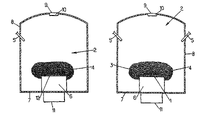
- n-type diamond is then obtained, as the sign of the Hall effect shows, this diamond having a high electrical conductivity at room temperature. If it is desired to n-dope only a fraction of the thickness of the boron-doped diamond, the hydrogen diffusion time is adjusted.
Landscapes
- Chemical & Material Sciences (AREA)
- Engineering & Computer Science (AREA)
- Crystallography & Structural Chemistry (AREA)
- Materials Engineering (AREA)
- Metallurgy (AREA)
- Organic Chemistry (AREA)
- Crystals, And After-Treatments Of Crystals (AREA)
- Chemical Vapour Deposition (AREA)
Applications Claiming Priority (4)
| Application Number | Priority Date | Filing Date | Title |
|---|---|---|---|
| FR0215453 | 2002-06-12 | ||
| FR0215453A FR2848335B1 (fr) | 2002-12-06 | 2002-12-06 | Procede d'elaboration de diamant de type n a haute conductivite electrique |
| PCT/FR2003/003592 WO2004053960A1 (fr) | 2002-12-06 | 2003-12-04 | Procede d'elaboration de diamant de type n a haute conductivite electrique |
| WOPCT/FR03/03592 | 2003-12-04 |
Related Parent Applications (1)
| Application Number | Title | Priority Date | Filing Date |
|---|---|---|---|
| PCT/FR2003/003592 Continuation WO2004053960A1 (fr) | 2002-12-06 | 2003-12-04 | Procede d'elaboration de diamant de type n a haute conductivite electrique |
Publications (2)
| Publication Number | Publication Date |
|---|---|
| US20050266606A1 US20050266606A1 (en) | 2005-12-01 |
| US7368317B2 true US7368317B2 (en) | 2008-05-06 |
Family
ID=32320061
Family Applications (1)
| Application Number | Title | Priority Date | Filing Date |
|---|---|---|---|
| US11/144,279 Expired - Fee Related US7368317B2 (en) | 2002-12-06 | 2005-06-03 | Method of producing an N-type diamond with high electrical conductivity |
Country Status (6)
| Country | Link |
|---|---|
| US (1) | US7368317B2 (fr) |
| EP (1) | EP1568072A1 (fr) |
| JP (1) | JP4823523B2 (fr) |
| AU (1) | AU2003298415A1 (fr) |
| FR (1) | FR2848335B1 (fr) |
| WO (1) | WO2004053960A1 (fr) |
Cited By (2)
| Publication number | Priority date | Publication date | Assignee | Title |
|---|---|---|---|---|
| WO2013019435A1 (fr) * | 2011-07-30 | 2013-02-07 | Akhan Technologies, Inc. | Système à semi-conducteurs diamants et procédé correspondant |
| US8933462B2 (en) | 2011-12-21 | 2015-01-13 | Akhan Semiconductor, Inc. | Method of fabricating diamond semiconductor and diamond semiconductor formed according to the method |
Families Citing this family (11)
| Publication number | Priority date | Publication date | Assignee | Title |
|---|---|---|---|---|
| CZ301547B6 (cs) * | 2008-08-29 | 2010-04-14 | Fyzikální ústav AV CR, v.v.i. | Zpusob dopování diamantu prenosem náboje z organických barviv |
| US8111724B2 (en) * | 2009-07-07 | 2012-02-07 | International Business Machines Corporation | Temperature control device for optoelectronic devices |
| SG179318A1 (en) * | 2010-09-27 | 2012-04-27 | Gemesis Company S Pte Ltd | Method for growing white color diamonds by using diborane and nitrogen in combination in a microwave plasma chemical vapor deposition system |
| GB201021855D0 (en) | 2010-12-23 | 2011-02-02 | Element Six Ltd | Microwave power delivery system for plasma reactors |
| GB201021853D0 (en) | 2010-12-23 | 2011-02-02 | Element Six Ltd | A microwave plasma reactor for manufacturing synthetic diamond material |
| GB201021870D0 (en) | 2010-12-23 | 2011-02-02 | Element Six Ltd | A microwave plasma reactor for manufacturing synthetic diamond material |
| KR101481928B1 (ko) | 2010-12-23 | 2015-01-21 | 엘리멘트 식스 리미티드 | 합성 다이아몬드 물질의 도핑을 제어하는 방법 |
| GB201021913D0 (en) | 2010-12-23 | 2011-02-02 | Element Six Ltd | Microwave plasma reactors and substrates for synthetic diamond manufacture |
| GB201021865D0 (en) | 2010-12-23 | 2011-02-02 | Element Six Ltd | A microwave plasma reactor for manufacturing synthetic diamond material |
| GB201021860D0 (en) | 2010-12-23 | 2011-02-02 | Element Six Ltd | A microwave plasma reactor for diamond synthesis |
| SG10201505413VA (en) | 2015-01-14 | 2016-08-30 | Iia Technologies Pte Ltd | Electronic device grade single crystal diamonds and method of producing the same |
Citations (8)
| Publication number | Priority date | Publication date | Assignee | Title |
|---|---|---|---|---|
| EP0543392A2 (fr) | 1991-11-21 | 1993-05-26 | Canon Kabushiki Kaisha | Dispositif semi-conducteur en diamant et méthode pour sa fabrication |
| JPH06151331A (ja) | 1992-11-12 | 1994-05-31 | Matsushita Electric Ind Co Ltd | 半導体ダイヤモンドの形成方法及び装置 |
| EP0646968A1 (fr) | 1993-09-30 | 1995-04-05 | Sony Corporation | Procédé pour la fabrication d'un semi-conducteur de diamant |
| JPH0920593A (ja) | 1995-07-02 | 1997-01-21 | Res Dev Corp Of Japan | 水素化アモルファスカーボンを用いた単結晶ダイヤモンドの合成法 |
| US5653800A (en) * | 1995-08-03 | 1997-08-05 | Eneco, Inc. | Method for producing N-type semiconducting diamond |
| JPH10247624A (ja) | 1997-03-05 | 1998-09-14 | Asahi Chem Ind Co Ltd | n型単結晶ダイヤモンドおよびその製造方法、人工ダイヤモンドの製造方法 |
| JPH10287966A (ja) | 1997-02-12 | 1998-10-27 | Toray Ind Inc | オイル薄膜の形成方法およびその薄膜を用いた蒸着製品の製造方法 |
| JP2000026194A (ja) | 1998-07-07 | 2000-01-25 | Japan Science & Technology Corp | 低抵抗n型ダイヤモンドの合成法 |
Family Cites Families (1)
| Publication number | Priority date | Publication date | Assignee | Title |
|---|---|---|---|---|
| JPH05139889A (ja) * | 1991-11-21 | 1993-06-08 | Canon Inc | ダイヤモンド結晶 |
-
2002
- 2002-12-06 FR FR0215453A patent/FR2848335B1/fr not_active Expired - Fee Related
-
2003
- 2003-12-04 WO PCT/FR2003/003592 patent/WO2004053960A1/fr not_active Ceased
- 2003-12-04 JP JP2004558172A patent/JP4823523B2/ja not_active Expired - Fee Related
- 2003-12-04 EP EP03796163A patent/EP1568072A1/fr not_active Withdrawn
- 2003-12-04 AU AU2003298415A patent/AU2003298415A1/en not_active Abandoned
-
2005
- 2005-06-03 US US11/144,279 patent/US7368317B2/en not_active Expired - Fee Related
Patent Citations (11)
| Publication number | Priority date | Publication date | Assignee | Title |
|---|---|---|---|---|
| EP0543392A2 (fr) | 1991-11-21 | 1993-05-26 | Canon Kabushiki Kaisha | Dispositif semi-conducteur en diamant et méthode pour sa fabrication |
| JPH06151331A (ja) | 1992-11-12 | 1994-05-31 | Matsushita Electric Ind Co Ltd | 半導体ダイヤモンドの形成方法及び装置 |
| EP0646968A1 (fr) | 1993-09-30 | 1995-04-05 | Sony Corporation | Procédé pour la fabrication d'un semi-conducteur de diamant |
| JPH0920593A (ja) | 1995-07-02 | 1997-01-21 | Res Dev Corp Of Japan | 水素化アモルファスカーボンを用いた単結晶ダイヤモンドの合成法 |
| US5891241A (en) | 1995-07-02 | 1999-04-06 | Research Development Corporation Of Japan | Synthesis of diamond single crystal from hydrogenated amorphous carbon |
| US5653800A (en) * | 1995-08-03 | 1997-08-05 | Eneco, Inc. | Method for producing N-type semiconducting diamond |
| JPH10287966A (ja) | 1997-02-12 | 1998-10-27 | Toray Ind Inc | オイル薄膜の形成方法およびその薄膜を用いた蒸着製品の製造方法 |
| JPH10247624A (ja) | 1997-03-05 | 1998-09-14 | Asahi Chem Ind Co Ltd | n型単結晶ダイヤモンドおよびその製造方法、人工ダイヤモンドの製造方法 |
| JP2000026194A (ja) | 1998-07-07 | 2000-01-25 | Japan Science & Technology Corp | 低抵抗n型ダイヤモンドの合成法 |
| EP1036863A1 (fr) | 1998-07-07 | 2000-09-20 | Japan Science and Technology Corporation | Procede de synthese de diamant de type n a faible resistance |
| US6340393B1 (en) | 1998-07-07 | 2002-01-22 | Japan Science And Technology Corporation | Method for synthesizing n-type diamond having low resistance |
Non-Patent Citations (15)
| Title |
|---|
| Ballutad, D. et al., "Diffusion and thermal stability of hydrogen in homoepitaxial CVD diamond films", Diamond and Related Materials, 9(2000), p. 1171-74. |
| Chevallier, J. et al., "Hydrogen-boron interactions in p-type diamond", Physical Review B., vol. 58, No. 12, pp. 7966-7969. |
| Chevallier, J., et al., "Hydrogen in Monocrystalline CVD Boron Doped Diamond", Phys. Stat. Sol., 174, 73, 1999, pp. 73-81. |
| Chevallier, J., et al., "Hydrogen in n-type diamond", Diamond and Related Materials, 11(2002), pp. 1566-1571. |
| Chevallier, J., et al., "Hydrogen-acceptor interactions in diamond", Diamond and Related Materials, 10(2001), pp. 399-404. |
| International Search Report for PCT/FR 03/03592, Apr. 12, 2003. |
| Koizumi, S., et al., "Phosphorus-doped chemical vapor deposition of diamond", Diamond and Related Materials, 9(2000), pp. 935-940. |
| Landstrass and Ravi, "Resistivity of chemical vapor deposited diamond films" Applied Physics Letters, Sep. 1989, pp. 975-976. |
| Popovici, G., et al., "Diffusion of boron, lithium, oxygen, hydrogen, and nitrogen in type IIa natural diamond", Journal of Applied Physics, May 15, 1995, pp. 5103-5106. |
| Popovici, G., et. al., "Diffusion of Impurities Under Bias in CVD Diamond Films", Mat. Res. Soc. Symp. Proc., vol. 339, 1994, pp. 601-606. |
| Preliminary Search Report for FA 630598/FR 0215453, Oct. 23, 2003. |
| Saguy, C., et al., "n-type diamond with high room temperature electrical conductivity by deuteration of boron doped diamond layers", Diamond and Related Materials, 13(2004), pp. 700-704. |
| Teukam, Z., et al., "Shallow donors with high n-type electrical conductivity in homoepitaxial deuterated boron-doped diamond layers", nature materials, vol. 2, Jul. 2003, pp. 482-486. |
| Teukam, Z., et. al., "Trap limited diffusion of hydrogen in boron-doped diamond", 12(2003), pp. 647-451. |
| Uzan-Saguy, C., et. al., "Hydrogen diffusion in B-ion-implanted and B-doped homo-epitaxial diamond: passivation of defects vs. passivation of B acceptors", Diamond and Related Materials, 10(2001), pp. 453-458. |
Cited By (3)
| Publication number | Priority date | Publication date | Assignee | Title |
|---|---|---|---|---|
| WO2013019435A1 (fr) * | 2011-07-30 | 2013-02-07 | Akhan Technologies, Inc. | Système à semi-conducteurs diamants et procédé correspondant |
| EP2737112A4 (fr) * | 2011-07-30 | 2015-03-25 | Akhan Technologies Inc | Système à semi-conducteurs diamants et procédé correspondant |
| US8933462B2 (en) | 2011-12-21 | 2015-01-13 | Akhan Semiconductor, Inc. | Method of fabricating diamond semiconductor and diamond semiconductor formed according to the method |
Also Published As
| Publication number | Publication date |
|---|---|
| JP2006508887A (ja) | 2006-03-16 |
| JP4823523B2 (ja) | 2011-11-24 |
| WO2004053960A1 (fr) | 2004-06-24 |
| AU2003298415A1 (en) | 2004-06-30 |
| EP1568072A1 (fr) | 2005-08-31 |
| FR2848335A1 (fr) | 2004-06-11 |
| US20050266606A1 (en) | 2005-12-01 |
| AU2003298415A8 (en) | 2004-06-30 |
| FR2848335B1 (fr) | 2005-10-07 |
Similar Documents
| Publication | Publication Date | Title |
|---|---|---|
| US7368317B2 (en) | Method of producing an N-type diamond with high electrical conductivity | |
| Nishizawa et al. | Silicon molecular layer epitaxy | |
| US10988858B2 (en) | Method for depositing a crystal layer at low temperatures, in particular a photoluminescent IV-IV layer on an IV substrate, and an optoelectronic component having such a layer | |
| US6015459A (en) | Method for doping semiconductor materials | |
| EP0368651A2 (fr) | Procédé et appareillage pour la croissance épitaxiale | |
| JP4873467B2 (ja) | オフ角を有する単結晶基板の製造方法 | |
| Zhong et al. | Selective low‐pressure chemical vapor deposition of Si1− x Ge x alloys in a rapid thermal processor using dichlorosilane and germane | |
| JP2008211222A (ja) | 半導体層中のドーパント拡散制御プロセス及びそれにより形成された半導体層 | |
| JP3929017B2 (ja) | 半導体層成長方法 | |
| Wang et al. | Effects of boron doping on the surface morphology and structural imperfections of diamond films | |
| Green et al. | High‐quality homoepitaxial silicon films deposited by rapid thermal chemical vapor deposition | |
| Sanganeria et al. | Boron Incorporation in Epitaxial Silicon Using Si2 H 6 and B 2 H 6 in an Ultrahigh Vacuum Rapid Thermal Chemical Vapor Deposition Reactor | |
| US7615390B2 (en) | Method and apparatus for forming expitaxial layers | |
| Racanelli et al. | Alternate Surface Cleaning Approaches for Ultra High Vacuum Chemical Vapor Deposition Epitaxy of Si and Ge x Si1− x | |
| Olson et al. | A mechanism of CVD diamond film growth deduced from the sequential deposition from sputtered carbon and atomic hydrogen | |
| Kinosky et al. | Low‐temperature growth of Ge x Si1− x/Si heterostructures on Si (100) by remote plasma‐enhanced chemical vapor deposition | |
| Comfort et al. | I n situ arsenic doping of epitaxial silicon at 800° C by plasma enhanced chemical vapor deposition | |
| JPS6370515A (ja) | 化学的気相成長方法及び化学的気相成長装置 | |
| CN117070917A (zh) | 一种掺杂金刚石制备方法 | |
| Caymax et al. | Low thermal budget chemical vapour deposition techniques for Si and SiGe | |
| CN120797194B (zh) | 氧化镓的外延生长方法 | |
| Monna et al. | Silicon thin films obtained by rapid thermal atmospheric pressure chemical vapour deposition | |
| CN121951689A (zh) | 一种n型半导体金刚石材料的制备方法 | |
| US20210210348A1 (en) | Method For Depositing A Crystal Layer At Low Temperatures, In Particular A Photoluminescent IV-IV Layer On An IV Substrate, And An Optoelectronic Component Having Such A Layer | |
| Rosenblad et al. | Influence of hydrogen desorption on the generation of defects in LEPECVD |
Legal Events
| Date | Code | Title | Description |
|---|---|---|---|
| AS | Assignment |
Owner name: UNIVERSITE DE VERSAILLES ST-QUENTIN EN YVELINES, F Free format text: ASSIGNMENT OF ASSIGNORS INTEREST;ASSIGNORS:CHEVALLIER, JACQUES P. MARIE;TEUKAM, ZEPHIRIN S.;BALLUTAUD, DOMINIQUE;REEL/FRAME:016546/0931 Effective date: 20050614 Owner name: CENTRE NATIONAL DE LA RECHERCHE SCIENTIFIQUE-CNRS, Free format text: ASSIGNMENT OF ASSIGNORS INTEREST;ASSIGNORS:CHEVALLIER, JACQUES P. MARIE;TEUKAM, ZEPHIRIN S.;BALLUTAUD, DOMINIQUE;REEL/FRAME:016546/0931 Effective date: 20050614 |
|
| FPAY | Fee payment |
Year of fee payment: 4 |
|
| REMI | Maintenance fee reminder mailed | ||
| LAPS | Lapse for failure to pay maintenance fees | ||
| STCH | Information on status: patent discontinuation |
Free format text: PATENT EXPIRED DUE TO NONPAYMENT OF MAINTENANCE FEES UNDER 37 CFR 1.362 |
|
| STCH | Information on status: patent discontinuation |
Free format text: PATENT EXPIRED DUE TO NONPAYMENT OF MAINTENANCE FEES UNDER 37 CFR 1.362 |
|
| FP | Lapsed due to failure to pay maintenance fee |
Effective date: 20160506 |