EP0543392A2 - Dispositif semi-conducteur en diamant et méthode pour sa fabrication - Google Patents
Dispositif semi-conducteur en diamant et méthode pour sa fabrication Download PDFInfo
- Publication number
- EP0543392A2 EP0543392A2 EP92119796A EP92119796A EP0543392A2 EP 0543392 A2 EP0543392 A2 EP 0543392A2 EP 92119796 A EP92119796 A EP 92119796A EP 92119796 A EP92119796 A EP 92119796A EP 0543392 A2 EP0543392 A2 EP 0543392A2
- Authority
- EP
- European Patent Office
- Prior art keywords
- diamond
- substrate
- crystal
- junction
- semiconductor device
- Prior art date
- Legal status (The legal status is an assumption and is not a legal conclusion. Google has not performed a legal analysis and makes no representation as to the accuracy of the status listed.)
- Ceased
Links
- 239000010432 diamond Substances 0.000 title claims abstract description 163
- 229910003460 diamond Inorganic materials 0.000 title claims abstract description 161
- 239000004065 semiconductor Substances 0.000 title claims abstract description 90
- 238000000034 method Methods 0.000 title claims abstract description 43
- 229910052744 lithium Inorganic materials 0.000 claims abstract description 32
- WHXSMMKQMYFTQS-UHFFFAOYSA-N Lithium Chemical compound [Li] WHXSMMKQMYFTQS-UHFFFAOYSA-N 0.000 claims abstract description 31
- 230000015572 biosynthetic process Effects 0.000 claims abstract description 28
- 229910052796 boron Inorganic materials 0.000 claims abstract description 22
- ZOXJGFHDIHLPTG-UHFFFAOYSA-N Boron Chemical compound [B] ZOXJGFHDIHLPTG-UHFFFAOYSA-N 0.000 claims abstract description 21
- 239000012535 impurity Substances 0.000 claims abstract description 16
- 238000003786 synthesis reaction Methods 0.000 claims abstract description 16
- 239000012808 vapor phase Substances 0.000 claims abstract description 11
- 230000008569 process Effects 0.000 claims abstract description 10
- 239000000758 substrate Substances 0.000 claims description 60
- 239000013078 crystal Substances 0.000 claims description 55
- 238000005401 electroluminescence Methods 0.000 claims description 10
- 238000004020 luminiscence type Methods 0.000 claims description 4
- VYPSYNLAJGMNEJ-UHFFFAOYSA-N silicon dioxide Inorganic materials O=[Si]=O VYPSYNLAJGMNEJ-UHFFFAOYSA-N 0.000 description 37
- 239000007789 gas Substances 0.000 description 28
- 238000006243 chemical reaction Methods 0.000 description 26
- 235000012239 silicon dioxide Nutrition 0.000 description 26
- LFQSCWFLJHTTHZ-UHFFFAOYSA-N Ethanol Chemical compound CCO LFQSCWFLJHTTHZ-UHFFFAOYSA-N 0.000 description 22
- 239000007788 liquid Substances 0.000 description 21
- 239000000463 material Substances 0.000 description 17
- 230000015556 catabolic process Effects 0.000 description 15
- 239000010453 quartz Substances 0.000 description 15
- VNWKTOKETHGBQD-UHFFFAOYSA-N methane Chemical compound C VNWKTOKETHGBQD-UHFFFAOYSA-N 0.000 description 14
- 238000005530 etching Methods 0.000 description 12
- 239000010408 film Substances 0.000 description 12
- OKTJSMMVPCPJKN-UHFFFAOYSA-N Carbon Chemical compound [C] OKTJSMMVPCPJKN-UHFFFAOYSA-N 0.000 description 11
- 229910052681 coesite Inorganic materials 0.000 description 11
- 229910052906 cristobalite Inorganic materials 0.000 description 11
- 239000000377 silicon dioxide Substances 0.000 description 11
- 229910052682 stishovite Inorganic materials 0.000 description 11
- 229910052905 tridymite Inorganic materials 0.000 description 11
- 239000006200 vaporizer Substances 0.000 description 11
- 229910052799 carbon Inorganic materials 0.000 description 10
- 235000019441 ethanol Nutrition 0.000 description 10
- 229910052739 hydrogen Inorganic materials 0.000 description 10
- 239000001257 hydrogen Substances 0.000 description 10
- 238000005268 plasma chemical vapour deposition Methods 0.000 description 10
- UFHFLCQGNIYNRP-UHFFFAOYSA-N Hydrogen Chemical compound [H][H] UFHFLCQGNIYNRP-UHFFFAOYSA-N 0.000 description 9
- 238000009413 insulation Methods 0.000 description 9
- CSCPPACGZOOCGX-UHFFFAOYSA-N Acetone Chemical compound CC(C)=O CSCPPACGZOOCGX-UHFFFAOYSA-N 0.000 description 8
- 238000000151 deposition Methods 0.000 description 7
- 150000002894 organic compounds Chemical class 0.000 description 7
- XKRFYHLGVUSROY-UHFFFAOYSA-N Argon Chemical compound [Ar] XKRFYHLGVUSROY-UHFFFAOYSA-N 0.000 description 6
- 238000005229 chemical vapour deposition Methods 0.000 description 6
- 238000002425 crystallisation Methods 0.000 description 6
- 238000001771 vacuum deposition Methods 0.000 description 6
- 239000010931 gold Substances 0.000 description 5
- 150000002431 hydrogen Chemical class 0.000 description 5
- 238000004519 manufacturing process Methods 0.000 description 5
- 229910052760 oxygen Inorganic materials 0.000 description 5
- 229910052710 silicon Inorganic materials 0.000 description 5
- XUIMIQQOPSSXEZ-UHFFFAOYSA-N Silicon Chemical compound [Si] XUIMIQQOPSSXEZ-UHFFFAOYSA-N 0.000 description 4
- QVGXLLKOCUKJST-UHFFFAOYSA-N atomic oxygen Chemical compound [O] QVGXLLKOCUKJST-UHFFFAOYSA-N 0.000 description 4
- ILAHWRKJUDSMFH-UHFFFAOYSA-N boron tribromide Chemical compound BrB(Br)Br ILAHWRKJUDSMFH-UHFFFAOYSA-N 0.000 description 4
- WTEOIRVLGSZEPR-UHFFFAOYSA-N boron trifluoride Chemical compound FB(F)F WTEOIRVLGSZEPR-UHFFFAOYSA-N 0.000 description 4
- 238000010438 heat treatment Methods 0.000 description 4
- 229910052751 metal Inorganic materials 0.000 description 4
- 239000002184 metal Substances 0.000 description 4
- 239000001301 oxygen Substances 0.000 description 4
- 239000012071 phase Substances 0.000 description 4
- 239000010703 silicon Substances 0.000 description 4
- UHOVQNZJYSORNB-UHFFFAOYSA-N Benzene Chemical compound C1=CC=CC=C1 UHOVQNZJYSORNB-UHFFFAOYSA-N 0.000 description 3
- KRHYYFGTRYWZRS-UHFFFAOYSA-N Fluorane Chemical compound F KRHYYFGTRYWZRS-UHFFFAOYSA-N 0.000 description 3
- OKKJLVBELUTLKV-UHFFFAOYSA-N Methanol Chemical compound OC OKKJLVBELUTLKV-UHFFFAOYSA-N 0.000 description 3
- 229910052782 aluminium Inorganic materials 0.000 description 3
- 229910052787 antimony Inorganic materials 0.000 description 3
- 229910052786 argon Inorganic materials 0.000 description 3
- 229910052785 arsenic Inorganic materials 0.000 description 3
- 229910002804 graphite Inorganic materials 0.000 description 3
- 239000010439 graphite Substances 0.000 description 3
- BHEPBYXIRTUNPN-UHFFFAOYSA-N hydridophosphorus(.) (triplet) Chemical compound [PH] BHEPBYXIRTUNPN-UHFFFAOYSA-N 0.000 description 3
- 238000010884 ion-beam technique Methods 0.000 description 3
- 230000009467 reduction Effects 0.000 description 3
- IJGRMHOSHXDMSA-UHFFFAOYSA-N Atomic nitrogen Chemical compound N#N IJGRMHOSHXDMSA-UHFFFAOYSA-N 0.000 description 2
- -1 B/C and Li/C Chemical compound 0.000 description 2
- 229910015900 BF3 Inorganic materials 0.000 description 2
- HEDRZPFGACZZDS-UHFFFAOYSA-N Chloroform Chemical compound ClC(Cl)Cl HEDRZPFGACZZDS-UHFFFAOYSA-N 0.000 description 2
- ATUOYWHBWRKTHZ-UHFFFAOYSA-N Propane Chemical compound CCC ATUOYWHBWRKTHZ-UHFFFAOYSA-N 0.000 description 2
- 229910002370 SrTiO3 Inorganic materials 0.000 description 2
- MCMNRKCIXSYSNV-UHFFFAOYSA-N Zirconium dioxide Chemical compound O=[Zr]=O MCMNRKCIXSYSNV-UHFFFAOYSA-N 0.000 description 2
- PNEYBMLMFCGWSK-UHFFFAOYSA-N aluminium oxide Inorganic materials [O-2].[O-2].[O-2].[Al+3].[Al+3] PNEYBMLMFCGWSK-UHFFFAOYSA-N 0.000 description 2
- 229910003481 amorphous carbon Inorganic materials 0.000 description 2
- WATWJIUSRGPENY-UHFFFAOYSA-N antimony atom Chemical compound [Sb] WATWJIUSRGPENY-UHFFFAOYSA-N 0.000 description 2
- RQNWIZPPADIBDY-UHFFFAOYSA-N arsenic atom Chemical compound [As] RQNWIZPPADIBDY-UHFFFAOYSA-N 0.000 description 2
- 230000004888 barrier function Effects 0.000 description 2
- KGBXLFKZBHKPEV-UHFFFAOYSA-N boric acid Chemical compound OB(O)O KGBXLFKZBHKPEV-UHFFFAOYSA-N 0.000 description 2
- 238000010276 construction Methods 0.000 description 2
- 229910052802 copper Inorganic materials 0.000 description 2
- 229910052593 corundum Inorganic materials 0.000 description 2
- 239000008710 crystal-8 Substances 0.000 description 2
- 238000006731 degradation reaction Methods 0.000 description 2
- 230000008021 deposition Effects 0.000 description 2
- 230000006866 deterioration Effects 0.000 description 2
- 239000003989 dielectric material Substances 0.000 description 2
- 238000001312 dry etching Methods 0.000 description 2
- 230000000694 effects Effects 0.000 description 2
- 229910052737 gold Inorganic materials 0.000 description 2
- 229910000449 hafnium oxide Inorganic materials 0.000 description 2
- 229960002050 hydrofluoric acid Drugs 0.000 description 2
- 230000006872 improvement Effects 0.000 description 2
- 238000005468 ion implantation Methods 0.000 description 2
- 238000007733 ion plating Methods 0.000 description 2
- KWGKDLIKAYFUFQ-UHFFFAOYSA-M lithium chloride Chemical compound [Li+].[Cl-] KWGKDLIKAYFUFQ-UHFFFAOYSA-M 0.000 description 2
- 150000002642 lithium compounds Chemical class 0.000 description 2
- 229910021421 monocrystalline silicon Inorganic materials 0.000 description 2
- 229910052757 nitrogen Inorganic materials 0.000 description 2
- 238000001020 plasma etching Methods 0.000 description 2
- 229920003229 poly(methyl methacrylate) Polymers 0.000 description 2
- 239000004926 polymethyl methacrylate Substances 0.000 description 2
- VZGDMQKNWNREIO-UHFFFAOYSA-N tetrachloromethane Chemical compound ClC(Cl)(Cl)Cl VZGDMQKNWNREIO-UHFFFAOYSA-N 0.000 description 2
- TXEYQDLBPFQVAA-UHFFFAOYSA-N tetrafluoromethane Chemical compound FC(F)(F)F TXEYQDLBPFQVAA-UHFFFAOYSA-N 0.000 description 2
- 230000001960 triggered effect Effects 0.000 description 2
- 229910052721 tungsten Inorganic materials 0.000 description 2
- 238000001039 wet etching Methods 0.000 description 2
- 229910001845 yogo sapphire Inorganic materials 0.000 description 2
- UOCLXMDMGBRAIB-UHFFFAOYSA-N 1,1,1-trichloroethane Chemical compound CC(Cl)(Cl)Cl UOCLXMDMGBRAIB-UHFFFAOYSA-N 0.000 description 1
- 229910052684 Cerium Inorganic materials 0.000 description 1
- OTMSDBZUPAUEDD-UHFFFAOYSA-N Ethane Chemical compound CC OTMSDBZUPAUEDD-UHFFFAOYSA-N 0.000 description 1
- VGGSQFUCUMXWEO-UHFFFAOYSA-N Ethene Chemical compound C=C VGGSQFUCUMXWEO-UHFFFAOYSA-N 0.000 description 1
- 239000005977 Ethylene Substances 0.000 description 1
- PXGOKWXKJXAPGV-UHFFFAOYSA-N Fluorine Chemical compound FF PXGOKWXKJXAPGV-UHFFFAOYSA-N 0.000 description 1
- GRYLNZFGIOXLOG-UHFFFAOYSA-N Nitric acid Chemical compound O[N+]([O-])=O GRYLNZFGIOXLOG-UHFFFAOYSA-N 0.000 description 1
- 229910003781 PbTiO3 Inorganic materials 0.000 description 1
- 229910052581 Si3N4 Inorganic materials 0.000 description 1
- UCKMPCXJQFINFW-UHFFFAOYSA-N Sulphide Chemical compound [S-2] UCKMPCXJQFINFW-UHFFFAOYSA-N 0.000 description 1
- 229910052771 Terbium Inorganic materials 0.000 description 1
- 229910052776 Thorium Inorganic materials 0.000 description 1
- 230000001133 acceleration Effects 0.000 description 1
- 150000001298 alcohols Chemical class 0.000 description 1
- HSFWRNGVRCDJHI-UHFFFAOYSA-N alpha-acetylene Natural products C#C HSFWRNGVRCDJHI-UHFFFAOYSA-N 0.000 description 1
- XAGFODPZIPBFFR-UHFFFAOYSA-N aluminium Chemical compound [Al] XAGFODPZIPBFFR-UHFFFAOYSA-N 0.000 description 1
- 229910052790 beryllium Inorganic materials 0.000 description 1
- 229910052797 bismuth Inorganic materials 0.000 description 1
- 229910052793 cadmium Inorganic materials 0.000 description 1
- 229910052792 caesium Inorganic materials 0.000 description 1
- 229910052791 calcium Inorganic materials 0.000 description 1
- WUKWITHWXAAZEY-UHFFFAOYSA-L calcium difluoride Chemical compound [F-].[F-].[Ca+2] WUKWITHWXAAZEY-UHFFFAOYSA-L 0.000 description 1
- 229910001634 calcium fluoride Inorganic materials 0.000 description 1
- 229910052804 chromium Inorganic materials 0.000 description 1
- 230000003749 cleanliness Effects 0.000 description 1
- 239000003086 colorant Substances 0.000 description 1
- 239000002131 composite material Substances 0.000 description 1
- 150000001875 compounds Chemical class 0.000 description 1
- 238000000354 decomposition reaction Methods 0.000 description 1
- 230000007547 defect Effects 0.000 description 1
- 230000006735 deficit Effects 0.000 description 1
- ZOCHARZZJNPSEU-UHFFFAOYSA-N diboron Chemical compound B#B ZOCHARZZJNPSEU-UHFFFAOYSA-N 0.000 description 1
- 238000007865 diluting Methods 0.000 description 1
- 239000006185 dispersion Substances 0.000 description 1
- 125000002534 ethynyl group Chemical group [H]C#C* 0.000 description 1
- 238000001704 evaporation Methods 0.000 description 1
- 230000001747 exhibiting effect Effects 0.000 description 1
- 229910052731 fluorine Inorganic materials 0.000 description 1
- 239000011737 fluorine Substances 0.000 description 1
- 229910052733 gallium Inorganic materials 0.000 description 1
- 239000011521 glass Substances 0.000 description 1
- PCHJSUWPFVWCPO-UHFFFAOYSA-N gold Chemical compound [Au] PCHJSUWPFVWCPO-UHFFFAOYSA-N 0.000 description 1
- 238000000227 grinding Methods 0.000 description 1
- CJNBYAVZURUTKZ-UHFFFAOYSA-N hafnium(iv) oxide Chemical compound O=[Hf]=O CJNBYAVZURUTKZ-UHFFFAOYSA-N 0.000 description 1
- 150000004820 halides Chemical class 0.000 description 1
- 239000001307 helium Substances 0.000 description 1
- 229910052734 helium Inorganic materials 0.000 description 1
- SWQJXJOGLNCZEY-UHFFFAOYSA-N helium atom Chemical compound [He] SWQJXJOGLNCZEY-UHFFFAOYSA-N 0.000 description 1
- 229930195733 hydrocarbon Natural products 0.000 description 1
- 150000002430 hydrocarbons Chemical class 0.000 description 1
- 230000001771 impaired effect Effects 0.000 description 1
- 229910052738 indium Inorganic materials 0.000 description 1
- 150000002500 ions Chemical class 0.000 description 1
- 229910052741 iridium Inorganic materials 0.000 description 1
- 229910052742 iron Inorganic materials 0.000 description 1
- CPLXHLVBOLITMK-UHFFFAOYSA-N magnesium oxide Inorganic materials [Mg]=O CPLXHLVBOLITMK-UHFFFAOYSA-N 0.000 description 1
- 229910052748 manganese Inorganic materials 0.000 description 1
- 239000000203 mixture Substances 0.000 description 1
- 238000012986 modification Methods 0.000 description 1
- 230000004048 modification Effects 0.000 description 1
- 229910052754 neon Inorganic materials 0.000 description 1
- GKAOGPIIYCISHV-UHFFFAOYSA-N neon atom Chemical compound [Ne] GKAOGPIIYCISHV-UHFFFAOYSA-N 0.000 description 1
- 229910052759 nickel Inorganic materials 0.000 description 1
- 229910052758 niobium Inorganic materials 0.000 description 1
- 229910017604 nitric acid Inorganic materials 0.000 description 1
- 239000003960 organic solvent Substances 0.000 description 1
- 229910052698 phosphorus Inorganic materials 0.000 description 1
- 229910052697 platinum Inorganic materials 0.000 description 1
- 229910052700 potassium Inorganic materials 0.000 description 1
- 239000001294 propane Substances 0.000 description 1
- 229910052702 rhenium Inorganic materials 0.000 description 1
- 229910052703 rhodium Inorganic materials 0.000 description 1
- 229910052701 rubidium Inorganic materials 0.000 description 1
- 229910052707 ruthenium Inorganic materials 0.000 description 1
- 238000005488 sandblasting Methods 0.000 description 1
- 229910052706 scandium Inorganic materials 0.000 description 1
- 229910052709 silver Inorganic materials 0.000 description 1
- 239000007787 solid Substances 0.000 description 1
- 229910052596 spinel Inorganic materials 0.000 description 1
- 239000011029 spinel Substances 0.000 description 1
- 238000005507 spraying Methods 0.000 description 1
- 238000004544 sputter deposition Methods 0.000 description 1
- 229910052712 strontium Inorganic materials 0.000 description 1
- 239000000126 substance Substances 0.000 description 1
- 229910052715 tantalum Inorganic materials 0.000 description 1
- PBCFLUZVCVVTBY-UHFFFAOYSA-N tantalum pentoxide Inorganic materials O=[Ta](=O)O[Ta](=O)=O PBCFLUZVCVVTBY-UHFFFAOYSA-N 0.000 description 1
- 229910052714 tellurium Inorganic materials 0.000 description 1
- 229910052716 thallium Inorganic materials 0.000 description 1
- 239000010409 thin film Substances 0.000 description 1
- 229910052718 tin Inorganic materials 0.000 description 1
- 229910052719 titanium Inorganic materials 0.000 description 1
- WFKWXMTUELFFGS-UHFFFAOYSA-N tungsten Chemical compound [W] WFKWXMTUELFFGS-UHFFFAOYSA-N 0.000 description 1
- 239000010937 tungsten Substances 0.000 description 1
- 238000007738 vacuum evaporation Methods 0.000 description 1
- 229910052720 vanadium Inorganic materials 0.000 description 1
- 238000005406 washing Methods 0.000 description 1
- 229910052727 yttrium Inorganic materials 0.000 description 1
- RUDFQVOCFDJEEF-UHFFFAOYSA-N yttrium(III) oxide Inorganic materials [O-2].[O-2].[O-2].[Y+3].[Y+3] RUDFQVOCFDJEEF-UHFFFAOYSA-N 0.000 description 1
- 229910052725 zinc Inorganic materials 0.000 description 1
- 229910052726 zirconium Inorganic materials 0.000 description 1
Images


Classifications
-
- H—ELECTRICITY
- H01—ELECTRIC ELEMENTS
- H01L—SEMICONDUCTOR DEVICES NOT COVERED BY CLASS H10
- H01L33/00—Semiconductor devices having potential barriers specially adapted for light emission; Processes or apparatus specially adapted for the manufacture or treatment thereof or of parts thereof; Details thereof
- H01L33/02—Semiconductor devices having potential barriers specially adapted for light emission; Processes or apparatus specially adapted for the manufacture or treatment thereof or of parts thereof; Details thereof characterised by the semiconductor bodies
- H01L33/26—Materials of the light emitting region
- H01L33/34—Materials of the light emitting region containing only elements of Group IV of the Periodic Table
- H01L33/343—Materials of the light emitting region containing only elements of Group IV of the Periodic Table characterised by the doping materials
-
- H—ELECTRICITY
- H01—ELECTRIC ELEMENTS
- H01L—SEMICONDUCTOR DEVICES NOT COVERED BY CLASS H10
- H01L21/00—Processes or apparatus adapted for the manufacture or treatment of semiconductor or solid state devices or of parts thereof
- H01L21/02—Manufacture or treatment of semiconductor devices or of parts thereof
- H01L21/02104—Forming layers
- H01L21/02365—Forming inorganic semiconducting materials on a substrate
- H01L21/02367—Substrates
- H01L21/0237—Materials
- H01L21/02373—Group 14 semiconducting materials
- H01L21/02381—Silicon, silicon germanium, germanium
-
- H—ELECTRICITY
- H01—ELECTRIC ELEMENTS
- H01L—SEMICONDUCTOR DEVICES NOT COVERED BY CLASS H10
- H01L21/00—Processes or apparatus adapted for the manufacture or treatment of semiconductor or solid state devices or of parts thereof
- H01L21/02—Manufacture or treatment of semiconductor devices or of parts thereof
- H01L21/02104—Forming layers
- H01L21/02365—Forming inorganic semiconducting materials on a substrate
- H01L21/02367—Substrates
- H01L21/0237—Materials
- H01L21/0242—Crystalline insulating materials
-
- H—ELECTRICITY
- H01—ELECTRIC ELEMENTS
- H01L—SEMICONDUCTOR DEVICES NOT COVERED BY CLASS H10
- H01L21/00—Processes or apparatus adapted for the manufacture or treatment of semiconductor or solid state devices or of parts thereof
- H01L21/02—Manufacture or treatment of semiconductor devices or of parts thereof
- H01L21/02104—Forming layers
- H01L21/02365—Forming inorganic semiconducting materials on a substrate
- H01L21/02367—Substrates
- H01L21/0237—Materials
- H01L21/02422—Non-crystalline insulating materials, e.g. glass, polymers
-
- H—ELECTRICITY
- H01—ELECTRIC ELEMENTS
- H01L—SEMICONDUCTOR DEVICES NOT COVERED BY CLASS H10
- H01L21/00—Processes or apparatus adapted for the manufacture or treatment of semiconductor or solid state devices or of parts thereof
- H01L21/02—Manufacture or treatment of semiconductor devices or of parts thereof
- H01L21/02104—Forming layers
- H01L21/02365—Forming inorganic semiconducting materials on a substrate
- H01L21/02518—Deposited layers
- H01L21/02521—Materials
- H01L21/02524—Group 14 semiconducting materials
- H01L21/02527—Carbon, e.g. diamond-like carbon
-
- H—ELECTRICITY
- H01—ELECTRIC ELEMENTS
- H01L—SEMICONDUCTOR DEVICES NOT COVERED BY CLASS H10
- H01L21/00—Processes or apparatus adapted for the manufacture or treatment of semiconductor or solid state devices or of parts thereof
- H01L21/02—Manufacture or treatment of semiconductor devices or of parts thereof
- H01L21/02104—Forming layers
- H01L21/02365—Forming inorganic semiconducting materials on a substrate
- H01L21/02518—Deposited layers
- H01L21/0257—Doping during depositing
- H01L21/02573—Conductivity type
- H01L21/02576—N-type
-
- H—ELECTRICITY
- H01—ELECTRIC ELEMENTS
- H01L—SEMICONDUCTOR DEVICES NOT COVERED BY CLASS H10
- H01L21/00—Processes or apparatus adapted for the manufacture or treatment of semiconductor or solid state devices or of parts thereof
- H01L21/02—Manufacture or treatment of semiconductor devices or of parts thereof
- H01L21/02104—Forming layers
- H01L21/02365—Forming inorganic semiconducting materials on a substrate
- H01L21/02518—Deposited layers
- H01L21/0257—Doping during depositing
- H01L21/02573—Conductivity type
- H01L21/02579—P-type
-
- H—ELECTRICITY
- H01—ELECTRIC ELEMENTS
- H01L—SEMICONDUCTOR DEVICES NOT COVERED BY CLASS H10
- H01L21/00—Processes or apparatus adapted for the manufacture or treatment of semiconductor or solid state devices or of parts thereof
- H01L21/02—Manufacture or treatment of semiconductor devices or of parts thereof
- H01L21/02104—Forming layers
- H01L21/02365—Forming inorganic semiconducting materials on a substrate
- H01L21/02518—Deposited layers
- H01L21/0257—Doping during depositing
- H01L21/02573—Conductivity type
- H01L21/02581—Transition metal or rare earth elements
-
- H—ELECTRICITY
- H01—ELECTRIC ELEMENTS
- H01L—SEMICONDUCTOR DEVICES NOT COVERED BY CLASS H10
- H01L21/00—Processes or apparatus adapted for the manufacture or treatment of semiconductor or solid state devices or of parts thereof
- H01L21/02—Manufacture or treatment of semiconductor devices or of parts thereof
- H01L21/02104—Forming layers
- H01L21/02365—Forming inorganic semiconducting materials on a substrate
- H01L21/02518—Deposited layers
- H01L21/02587—Structure
- H01L21/0259—Microstructure
- H01L21/02595—Microstructure polycrystalline
-
- H—ELECTRICITY
- H01—ELECTRIC ELEMENTS
- H01L—SEMICONDUCTOR DEVICES NOT COVERED BY CLASS H10
- H01L21/00—Processes or apparatus adapted for the manufacture or treatment of semiconductor or solid state devices or of parts thereof
- H01L21/02—Manufacture or treatment of semiconductor devices or of parts thereof
- H01L21/02104—Forming layers
- H01L21/02365—Forming inorganic semiconducting materials on a substrate
- H01L21/02612—Formation types
- H01L21/02617—Deposition types
- H01L21/0262—Reduction or decomposition of gaseous compounds, e.g. CVD
-
- H—ELECTRICITY
- H01—ELECTRIC ELEMENTS
- H01L—SEMICONDUCTOR DEVICES NOT COVERED BY CLASS H10
- H01L21/00—Processes or apparatus adapted for the manufacture or treatment of semiconductor or solid state devices or of parts thereof
- H01L21/02—Manufacture or treatment of semiconductor devices or of parts thereof
- H01L21/02104—Forming layers
- H01L21/02365—Forming inorganic semiconducting materials on a substrate
- H01L21/02612—Formation types
- H01L21/02617—Deposition types
- H01L21/02636—Selective deposition, e.g. simultaneous growth of mono- and non-monocrystalline semiconductor materials
- H01L21/02639—Preparation of substrate for selective deposition
- H01L21/02645—Seed materials
-
- H—ELECTRICITY
- H01—ELECTRIC ELEMENTS
- H01L—SEMICONDUCTOR DEVICES NOT COVERED BY CLASS H10
- H01L29/00—Semiconductor devices specially adapted for rectifying, amplifying, oscillating or switching and having potential barriers; Capacitors or resistors having potential barriers, e.g. a PN-junction depletion layer or carrier concentration layer; Details of semiconductor bodies or of electrodes thereof ; Multistep manufacturing processes therefor
- H01L29/02—Semiconductor bodies ; Multistep manufacturing processes therefor
- H01L29/12—Semiconductor bodies ; Multistep manufacturing processes therefor characterised by the materials of which they are formed
- H01L29/16—Semiconductor bodies ; Multistep manufacturing processes therefor characterised by the materials of which they are formed including, apart from doping materials or other impurities, only elements of Group IV of the Periodic Table
- H01L29/1602—Diamond
-
- H—ELECTRICITY
- H01—ELECTRIC ELEMENTS
- H01L—SEMICONDUCTOR DEVICES NOT COVERED BY CLASS H10
- H01L29/00—Semiconductor devices specially adapted for rectifying, amplifying, oscillating or switching and having potential barriers; Capacitors or resistors having potential barriers, e.g. a PN-junction depletion layer or carrier concentration layer; Details of semiconductor bodies or of electrodes thereof ; Multistep manufacturing processes therefor
- H01L29/02—Semiconductor bodies ; Multistep manufacturing processes therefor
- H01L29/12—Semiconductor bodies ; Multistep manufacturing processes therefor characterised by the materials of which they are formed
- H01L29/16—Semiconductor bodies ; Multistep manufacturing processes therefor characterised by the materials of which they are formed including, apart from doping materials or other impurities, only elements of Group IV of the Periodic Table
- H01L29/167—Semiconductor bodies ; Multistep manufacturing processes therefor characterised by the materials of which they are formed including, apart from doping materials or other impurities, only elements of Group IV of the Periodic Table further characterised by the doping material
-
- H—ELECTRICITY
- H01—ELECTRIC ELEMENTS
- H01L—SEMICONDUCTOR DEVICES NOT COVERED BY CLASS H10
- H01L33/00—Semiconductor devices having potential barriers specially adapted for light emission; Processes or apparatus specially adapted for the manufacture or treatment thereof or of parts thereof; Details thereof
- H01L33/0004—Devices characterised by their operation
- H01L33/0033—Devices characterised by their operation having Schottky barriers
-
- H—ELECTRICITY
- H01—ELECTRIC ELEMENTS
- H01L—SEMICONDUCTOR DEVICES NOT COVERED BY CLASS H10
- H01L33/00—Semiconductor devices having potential barriers specially adapted for light emission; Processes or apparatus specially adapted for the manufacture or treatment thereof or of parts thereof; Details thereof
- H01L33/005—Processes
- H01L33/0054—Processes for devices with an active region comprising only group IV elements
Definitions
- the known semiconductor devices using diamond could not provide satisfactory characteristics.
- the level of the operation current is undesirably limited when the devices have pn junctions which are basic constructions in semiconductor devices. This is mainly attributed to the fact that n-type semiconductors having low resistance level can hardly be obtained with diamond.
- an object of the present invention is to provide a pn junction diamond semiconductor which can operate with a large electric current and which exhibits superior pn junction characteristics, as well as high durability.
- Another object of the present invention is to provide an electroluminescence device having high insulation dielectric strength.
- Production of the p-type semiconductor employs introduction of boron into diamond. This can be done, for example, by using a material gas containing diborane (B2H6), boron trifluoride (BF3), or boron tribromide (BBr3). Alternatively, when a liquid organic compound such as acetone or alcohol is used as a carbon source, boric acid (H3BO3) is added into the liquid organic compound.
- B2H6 diborane
- BF3 boron trifluoride
- BBr3 boron tribromide
- the breakdown triggered by the underlying insulating layer is considered to be attributable to the aforesaid damage of the underlying insulating layers 12, 13 incurred during formation of the diamond luminescent layer 14 thereon.
- the diamond luminescent layer 14 is formed at high temperature of 800 to 900°C by microwave plasma CVD, employing plasma of a material gas containing hydrogen, methane and oxygen. Consequently, the insulating layers tend to be partly damaged or etched, with the result that the insulating nature is seriously impaired to trigger breakdown when a voltage is applied thereto. This problem would be overcome by increasing the thickness of the insulating layer, but such a measure is not recommenced because the increased thickness of the insulating layer reduces adhesion between the insulating layer and the underlying substrate 11.
- the breakdown occurring at the grain boundaries is considered to be attributable to presence of amorphous or graphite phase which exists in the grain boundary of the diamond luminescent layer.
- the diamond crystal possesses a very high dielectric strength, e.g., several MV/cm or higher, but amorphous carbon generally has a dielectric strength which is as small as 1/100 to 1/1000 that of diamond.
- graphite phase is electrically conductive. These non-diamond phases very often appear in grain boundaries, triggering breakdown of insulation under application of a voltage.
- the above-described abrading treatment is conducted preferably by employing diamond grains, but may be effected by supersonic treatment or by sand blasting.
- abrading of an Si single crystal substrate by a lateral grinding device employing diamond grains of 1 ⁇ m or smaller causes production of nuclei at a density of 107/cm2 or greater.
- the abrading with supersonic wave is preferably effected by immersing the substrate in a liquid in which grains of 1 to 50 mm are dispersed, and applying supersonic wave by. for example, a supersonic washing device for a period of 5 minutes to 4 hours, preferably from 10 minutes to 2 hours. With this method also, it is possible to obtain a nuclei density of 107/cm2 or greater.
- Luminescence takes place in a portion of the device near the Schottky electrode 3 when a forward voltage is applied by a D.C. power supply 5 between the Schottky electrode 3 and the ohmic electrode 4.
- the term "forward voltage” in this case means a voltage applied such that, when the diamond crystal layer 2 is a p-type semiconductor, the Schottky junction electrode receives a negative voltage while the ohmic junction electrode 4 receives a positive voltage.
- the forward voltage means such a voltage that the Schottky junction electrode is a positive electrode, while the ohmic junction electrode is a negative electrode.
- numeral 7 denotes an insulating layer preferably made of a material which has high transparency and breakdown voltage in visible wavelength region and which has a large dielectric constant.
- dielectric materials such as SiO2, Y2O3, HfO2, Si3N4, Al2O3, Ta2O5, PbTiO3, BaTa2O6 and SrTiO3.
- the insulating layer 7 is formed to have a thickness of 500 to 5000 A by a method such as vacuum evaporation, ion plating,sputtering, spraying and CVD.
- PMMA polymethyl methacrylate
- the masked surface of the substrate 1 was etched to a depth of approximately 1200 ⁇ by using an Ar ion beam etching apparatus.
- the etching was conducted for a period of 10 minutes at an acceleration voltage of 1 kV.
- an Al electrode as a Schottky electrode 3 and a Au electrode as an ohmic electrode 4 were formed with a thickness of approximately 1000 ⁇ on each diamond crystal 2 by a vacuum deposition method in such a manner that these electrodes 3 and 4 did not overlap each other.
- a quartz substrate 6 (diameter: 25 mm, thickness: 0.5 mm) was subjected to the same abrading, resist-pattern forming, and etching as those in Example 1.
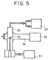
- Fig. 6 shows an example of an apparatus for forming a diamond semiconductor.
- the apparatus is a heat filament CVD apparatus, and includes a quartz reaction tube 61 disposed in an electric furnace 62, a tungsten filament 63 disposed in the reaction tube 61, a gas inlet tube 65, a flowmeter 66 for adjusting the gas flow rate, a first liquid vaporizer 67a for heating and gasifying a liquid organic compound containing lithium, a second liquid vaporizer 67b for heating and gasifying a liquid organic compound containing boron, a valve 68, a hydrogen gas cylinder 69, and an exhaust port 70 connected to a pressure adjusting valve and an exhaustion system (neither of which are shown).
- the apparatus is shown in the state where a substrate 64 is already set.
- the pressure adjusting valve was used to adjust the internal pressure within the reaction tube 61 to 50 Torr.
- the filament 63 was supplied with power from a power supply, not shown, and was red-heated to approximately 2100°C.
- the red-heated filament 63 caused decomposition of ethanol and hydrogen, thereby forming n-type diamond containing lithium on the substrate 64.
- the diode characteristics thus evaluated are indicated by solid lines in Fig. 7.
- the ratio in magnitude between forward current and backward current was at least 108.
- the leakage current in the backward direction was not more than 10 ⁇ 10 A, and the break-down voltage was not less than 250 V. Thus, very good diode characteristics were obtained.
- a single-crystal silicon substrate 84 of the same type as that used in Example 11 was placed inside the quartz reaction tube 81.
- the interior of the quartz reaction tube 81 was evacuated to 2 x 10 ⁇ 3 Torr by the exhaustion system. Thereafter, the first, second and third gas cylinders 88a, 88b and 88c as well as the flowmeters 86a, 86b and 86c were used to introduce, into the quartz reaction tube 81, hydrogen, methane, and diborane at flow rates of 200 ml/min, 0.75 ml/min and 40 ml/min, respectively.
- the pressure adjusting valve was used to adjust the internal pressure within the reaction tube 81 to 60 Torr.
- the microwave generator 82 was used to apply microwave to the quartz reaction tube 81 (output: 0.8 kW).
- plasma was generated, thereby forming p-type diamond containing boron on the substrate 84.
- a resist pattern was formed on a part of each diamond crystal 97 by a known photolithographic method, a SiO2 film with a thickness of 1000 ⁇ was formed through the resist by a known vacuum deposition method, and thereafter the resist was removed, thereby depositing SiO2 on a part of each diamond crystal 97.
Landscapes
- Engineering & Computer Science (AREA)
- Power Engineering (AREA)
- Microelectronics & Electronic Packaging (AREA)
- Computer Hardware Design (AREA)
- Manufacturing & Machinery (AREA)
- General Physics & Mathematics (AREA)
- Physics & Mathematics (AREA)
- Condensed Matter Physics & Semiconductors (AREA)
- Chemical & Material Sciences (AREA)
- Crystallography & Structural Chemistry (AREA)
- Materials Engineering (AREA)
- Ceramic Engineering (AREA)
- Inorganic Chemistry (AREA)
- Led Devices (AREA)
- Crystals, And After-Treatments Of Crystals (AREA)
Applications Claiming Priority (4)
| Application Number | Priority Date | Filing Date | Title |
|---|---|---|---|
| JP331591/91 | 1991-11-21 | ||
| JP33159191A JPH05139889A (ja) | 1991-11-21 | 1991-11-21 | ダイヤモンド結晶 |
| JP339371/91 | 1991-11-29 | ||
| JP33937191A JPH05152604A (ja) | 1991-11-29 | 1991-11-29 | ダイヤモンド半導体装置及びその製造方法 |
Publications (2)
| Publication Number | Publication Date |
|---|---|
| EP0543392A2 true EP0543392A2 (fr) | 1993-05-26 |
| EP0543392A3 EP0543392A3 (en) | 1993-10-20 |
Family
ID=26573899
Family Applications (1)
| Application Number | Title | Priority Date | Filing Date |
|---|---|---|---|
| EP19920119796 Ceased EP0543392A3 (en) | 1991-11-21 | 1992-11-20 | Diamond semiconductor device and method of producing the same |
Country Status (2)
| Country | Link |
|---|---|
| US (1) | US5541423A (fr) |
| EP (1) | EP0543392A3 (fr) |
Cited By (2)
| Publication number | Priority date | Publication date | Assignee | Title |
|---|---|---|---|---|
| EP0646968A1 (fr) * | 1993-09-30 | 1995-04-05 | Sony Corporation | Procédé pour la fabrication d'un semi-conducteur de diamant |
| FR2848335A1 (fr) * | 2002-12-06 | 2004-06-11 | Centre Nat Rech Scient | Procede d'elaboration de diamant de type n a haute conductivite electrique |
Families Citing this family (25)
| Publication number | Priority date | Publication date | Assignee | Title |
|---|---|---|---|---|
| US5463271A (en) * | 1993-07-09 | 1995-10-31 | Silicon Video Corp. | Structure for enhancing electron emission from carbon-containing cathode |
| US5961718A (en) * | 1995-10-16 | 1999-10-05 | National Science Council | Process for selectively depositing diamond films |
| US6356014B2 (en) | 1997-03-27 | 2002-03-12 | Candescent Technologies Corporation | Electron emitters coated with carbon containing layer |
| DE19718618C2 (de) * | 1997-05-02 | 1999-12-02 | Daimler Chrysler Ag | Komposit-Struktur mit einem mehrere mikroelektronische Bauteile und eine Diamantschicht aufweisenden Wachstums-Substrat sowie Verfahren zur Herstellung der Komposit-Struktur |
| US6582513B1 (en) * | 1998-05-15 | 2003-06-24 | Apollo Diamond, Inc. | System and method for producing synthetic diamond |
| US6858080B2 (en) * | 1998-05-15 | 2005-02-22 | Apollo Diamond, Inc. | Tunable CVD diamond structures |
| JP4421745B2 (ja) * | 2001-12-28 | 2010-02-24 | 東洋炭素株式会社 | 半導体ダイヤモンド合成用黒鉛材及び半導体ダイヤモンドの製造方法 |
| US7402835B2 (en) * | 2002-07-18 | 2008-07-22 | Chevron U.S.A. Inc. | Heteroatom-containing diamondoid transistors |
| US7501330B2 (en) * | 2002-12-05 | 2009-03-10 | Intel Corporation | Methods of forming a high conductivity diamond film and structures formed thereby |
| US7224532B2 (en) * | 2002-12-06 | 2007-05-29 | Chevron U.S.A. Inc. | Optical uses diamondoid-containing materials |
| JP2004214264A (ja) * | 2002-12-27 | 2004-07-29 | Sumitomo Electric Ind Ltd | 低抵抗n型半導体ダイヤモンドおよびその製造方法 |
| US20050019955A1 (en) * | 2003-07-23 | 2005-01-27 | Dahl Jeremy E. | Luminescent heterodiamondoids as biological labels |
| EP1667188A4 (fr) * | 2003-09-16 | 2008-09-10 | Sumitomo Electric Industries | Emetteur d'electrons en diamant et source de faisceau electronique l'utilisant |
| US20050181210A1 (en) * | 2004-02-13 | 2005-08-18 | Doering Patrick J. | Diamond structure separation |
| US20060163584A1 (en) * | 2005-01-26 | 2006-07-27 | Robert Linares | Boron-doped diamond semiconductor |
| DE102005028216A1 (de) | 2005-06-17 | 2006-12-28 | Siemens Ag | Vorrichtung und Verfahren für die Computertomographie |
| JP4908409B2 (ja) | 2005-06-20 | 2012-04-04 | 日本電信電話株式会社 | ダイヤモンド半導体素子およびその製造方法 |
| US7799600B2 (en) * | 2007-05-31 | 2010-09-21 | Chien-Min Sung | Doped diamond LED devices and associated methods |
| JP5539968B2 (ja) * | 2008-05-05 | 2014-07-02 | カーネギー インスチチューション オブ ワシントン | 超靭性の単結晶ホウ素ドープダイヤモンド |
| WO2010068419A2 (fr) * | 2008-11-25 | 2010-06-17 | Carnegie Institution Of Washington | Production de diamant monocristallin par dépôt en phase vapeur à vitesse de croissance rapide |
| US9421738B2 (en) * | 2013-08-12 | 2016-08-23 | The United States Of America, As Represented By The Secretary Of The Navy | Chemically stable visible light photoemission electron source |
| US10211049B2 (en) * | 2015-08-07 | 2019-02-19 | North Carolina State University | Synthesis and processing of pure and NV nanodiamonds and other nanostructures |
| WO2018005619A1 (fr) | 2016-06-28 | 2018-01-04 | North Carolina State University | Synthèse et traitement de nanodiamants purs et nv et d'autres nanostructures pour des applications de calcul quantique et de détection magnétique |
| US11932929B2 (en) * | 2017-08-21 | 2024-03-19 | George Edward Parris | Method and materials for creating patterns of carbon and/or other elements on substrates or within liquid or frozen media by directed energy deposition of carbon and other elements |
| DE102021123907A1 (de) | 2021-09-15 | 2023-03-16 | Universität Siegen, Körperschaft des öffentlichen Rechts | LED und Herstellungsverfahren dafür |
Citations (2)
| Publication number | Priority date | Publication date | Assignee | Title |
|---|---|---|---|---|
| GB2240428A (en) * | 1990-01-26 | 1991-07-31 | Kobe Steel Ltd | Semiconducting diamond light emitting element |
| US5051785A (en) * | 1989-06-22 | 1991-09-24 | Advanced Technology Materials, Inc. | N-type semiconducting diamond, and method of making the same |
Family Cites Families (12)
| Publication number | Priority date | Publication date | Assignee | Title |
|---|---|---|---|---|
| JPS59208821A (ja) * | 1983-05-13 | 1984-11-27 | Sumitomo Electric Ind Ltd | 気相合成によるダイヤモンド半導体およびその製造方法 |
| JPS59213126A (ja) * | 1983-05-19 | 1984-12-03 | Sumitomo Electric Ind Ltd | ダイヤモンド半導体素子の製造法 |
| JPS60246627A (ja) * | 1984-05-21 | 1985-12-06 | Sumitomo Electric Ind Ltd | ダイヤモンド半導体素子 |
| JP2650730B2 (ja) * | 1988-08-08 | 1997-09-03 | シャープ株式会社 | 炭化珪素半導体を用いたpn接合型発光ダイオード |
| JPH0397275A (ja) * | 1989-09-09 | 1991-04-23 | Katsunobu Maeda | 炭化硅素の青色発光ダイオード素子 |
| EP0420188A1 (fr) * | 1989-09-27 | 1991-04-03 | Sumitomo Electric Industries, Ltd. | Structure semi-conductrice à hétérojonction |
| JP2775903B2 (ja) * | 1989-10-04 | 1998-07-16 | 住友電気工業株式会社 | ダイヤモンド半導体素子 |
| JP2509713B2 (ja) * | 1989-10-18 | 1996-06-26 | シャープ株式会社 | 炭化珪素半導体装置およびその製造方法 |
| JP3104229B2 (ja) * | 1989-11-28 | 2000-10-30 | ソニー株式会社 | ビデオカメラ用外部同期装置 |
| US5243199A (en) * | 1990-01-19 | 1993-09-07 | Sumitomo Electric Industries, Ltd. | High frequency device |
| JP2730271B2 (ja) * | 1990-03-07 | 1998-03-25 | 住友電気工業株式会社 | 半導体装置 |
| US5285078A (en) * | 1992-01-24 | 1994-02-08 | Nippon Steel Corporation | Light emitting element with employment of porous silicon and optical device utilizing light emitting element |
-
1992
- 1992-11-20 EP EP19920119796 patent/EP0543392A3/en not_active Ceased
-
1994
- 1994-07-20 US US08/278,104 patent/US5541423A/en not_active Expired - Lifetime
Patent Citations (2)
| Publication number | Priority date | Publication date | Assignee | Title |
|---|---|---|---|---|
| US5051785A (en) * | 1989-06-22 | 1991-09-24 | Advanced Technology Materials, Inc. | N-type semiconducting diamond, and method of making the same |
| GB2240428A (en) * | 1990-01-26 | 1991-07-31 | Kobe Steel Ltd | Semiconducting diamond light emitting element |
Non-Patent Citations (1)
| Title |
|---|
| APPLIED PHYSICS LETTERS vol. 53, no. 7, 15 August 1988, NEW YORK US pages 586 - 588 G.S. GILDENBLAT ET AL. 'ELECTRICAL CHARACTERISTICS OF SCHOTTKY DIODES FABRICATED USING PLASMA ASSISTED CHEMICAL VAPOR DEPOSITED DIAMOND FILMS' * |
Cited By (5)
| Publication number | Priority date | Publication date | Assignee | Title |
|---|---|---|---|---|
| EP0646968A1 (fr) * | 1993-09-30 | 1995-04-05 | Sony Corporation | Procédé pour la fabrication d'un semi-conducteur de diamant |
| US5508208A (en) * | 1993-09-30 | 1996-04-16 | Sony Corporation | Method of manufacturing diamond semiconductor |
| FR2848335A1 (fr) * | 2002-12-06 | 2004-06-11 | Centre Nat Rech Scient | Procede d'elaboration de diamant de type n a haute conductivite electrique |
| WO2004053960A1 (fr) * | 2002-12-06 | 2004-06-24 | Centre National De La Recherche Scientifique - Cnrs | Procede d'elaboration de diamant de type n a haute conductivite electrique |
| US7368317B2 (en) | 2002-12-06 | 2008-05-06 | Centre National De La Recherche Scientifique-Cnrs | Method of producing an N-type diamond with high electrical conductivity |
Also Published As
| Publication number | Publication date |
|---|---|
| EP0543392A3 (en) | 1993-10-20 |
| US5541423A (en) | 1996-07-30 |
Similar Documents
| Publication | Publication Date | Title |
|---|---|---|
| EP0543392A2 (fr) | Dispositif semi-conducteur en diamant et méthode pour sa fabrication | |
| US5632812A (en) | Diamond electronic device and process for producing the same | |
| Gildenblat et al. | The electrical properties and device applications of homoepitaxial and polycrystalline diamond films | |
| US5620557A (en) | Sapphireless group III nitride semiconductor and method for making same | |
| CA2054242C (fr) | Dispositif luminescent au nitrure de gallium | |
| US5747118A (en) | Plasma enhanced chemical transport process for forming diamond films | |
| EP0377320B1 (fr) | Appareil émetteur de lumière au moyen d'un champ électrique | |
| Khan et al. | Electrical properties and ion implantation of epitaxial GaN, grown by low pressure metalorganic chemical vapor deposition | |
| US5897924A (en) | Process for depositing adherent diamond thin films | |
| JP3428984B2 (ja) | 安定化層及びその製法 | |
| EP0390209B1 (fr) | Dispositif émetteur de lumière en diamant | |
| US5034784A (en) | Diamond electric device on silicon | |
| US7063742B1 (en) | N-type semiconductor diamond and its fabrication method | |
| US5612548A (en) | Diamond light-emitting element | |
| Sugino et al. | Electron emission characteristics of metal/diamond field emitters | |
| Futagi et al. | Highly conductive and wide optical band gap n‐type μc‐SiC prepared by electron cyclotron resonance plasma‐enhanced chemical vapor deposition | |
| JPH05152604A (ja) | ダイヤモンド半導体装置及びその製造方法 | |
| EP0244874A2 (fr) | Matériau luminescent, son procédé de production, et élément semi-conducteur luminescent en faisant usage | |
| JPH11185964A (ja) | 有機発光素子及びその製造方法 | |
| Sekiguchi et al. | Characterization of a diamond pn junction using electron-beam-induced current and cathodoluminescence | |
| Makino et al. | Strong excitonic emission from (001)-oriented diamond p–n junction | |
| Lau et al. | a-SiC: H thin film visible light-emitting diodes with highly conductive wide band gap a-SiC: H as the carrier injection layers | |
| EP0822268B1 (fr) | Procédé de production d'un revêtement de diamant adhérent | |
| Mino et al. | Plasma‐assisted metalorganic chemical vapor deposition of ZnSe films | |
| Futagi et al. | An amorphous SiC thin film visible light-emitting diode with a μc-SiC: H electron injector |
Legal Events
| Date | Code | Title | Description |
|---|---|---|---|
| PUAI | Public reference made under article 153(3) epc to a published international application that has entered the european phase |
Free format text: ORIGINAL CODE: 0009012 |
|
| AK | Designated contracting states |
Kind code of ref document: A2 Designated state(s): DE FR GB |
|
| PUAL | Search report despatched |
Free format text: ORIGINAL CODE: 0009013 |
|
| AK | Designated contracting states |
Kind code of ref document: A3 Designated state(s): DE FR GB |
|
| 17P | Request for examination filed |
Effective date: 19940302 |
|
| 17Q | First examination report despatched |
Effective date: 19960228 |
|
| STAA | Information on the status of an ep patent application or granted ep patent |
Free format text: STATUS: THE APPLICATION HAS BEEN REFUSED |
|
| 18R | Application refused |
Effective date: 20021112 |