US7321459B2 - Image display device and method - Google Patents
Image display device and method Download PDFInfo
- Publication number
- US7321459B2 US7321459B2 US10/506,533 US50653305A US7321459B2 US 7321459 B2 US7321459 B2 US 7321459B2 US 50653305 A US50653305 A US 50653305A US 7321459 B2 US7321459 B2 US 7321459B2
- Authority
- US
- United States
- Prior art keywords
- liquid powder
- display device
- image display
- particle size
- powder
- Prior art date
- Legal status (The legal status is an assumption and is not a legal conclusion. Google has not performed a legal analysis and makes no representation as to the accuracy of the status listed.)
- Expired - Fee Related, expires
Links
Images


Classifications
-
- G—PHYSICS
- G02—OPTICS
- G02F—OPTICAL DEVICES OR ARRANGEMENTS FOR THE CONTROL OF LIGHT BY MODIFICATION OF THE OPTICAL PROPERTIES OF THE MEDIA OF THE ELEMENTS INVOLVED THEREIN; NON-LINEAR OPTICS; FREQUENCY-CHANGING OF LIGHT; OPTICAL LOGIC ELEMENTS; OPTICAL ANALOGUE/DIGITAL CONVERTERS
- G02F1/00—Devices or arrangements for the control of the intensity, colour, phase, polarisation or direction of light arriving from an independent light source, e.g. switching, gating or modulating; Non-linear optics
- G02F1/01—Devices or arrangements for the control of the intensity, colour, phase, polarisation or direction of light arriving from an independent light source, e.g. switching, gating or modulating; Non-linear optics for the control of the intensity, phase, polarisation or colour
- G02F1/165—Devices or arrangements for the control of the intensity, colour, phase, polarisation or direction of light arriving from an independent light source, e.g. switching, gating or modulating; Non-linear optics for the control of the intensity, phase, polarisation or colour based on translational movement of particles in a fluid under the influence of an applied field
- G02F1/166—Devices or arrangements for the control of the intensity, colour, phase, polarisation or direction of light arriving from an independent light source, e.g. switching, gating or modulating; Non-linear optics for the control of the intensity, phase, polarisation or colour based on translational movement of particles in a fluid under the influence of an applied field characterised by the electro-optical or magneto-optical effect
- G02F1/1671—Devices or arrangements for the control of the intensity, colour, phase, polarisation or direction of light arriving from an independent light source, e.g. switching, gating or modulating; Non-linear optics for the control of the intensity, phase, polarisation or colour based on translational movement of particles in a fluid under the influence of an applied field characterised by the electro-optical or magneto-optical effect involving dry toners
-
- G—PHYSICS
- G02—OPTICS
- G02F—OPTICAL DEVICES OR ARRANGEMENTS FOR THE CONTROL OF LIGHT BY MODIFICATION OF THE OPTICAL PROPERTIES OF THE MEDIA OF THE ELEMENTS INVOLVED THEREIN; NON-LINEAR OPTICS; FREQUENCY-CHANGING OF LIGHT; OPTICAL LOGIC ELEMENTS; OPTICAL ANALOGUE/DIGITAL CONVERTERS
- G02F1/00—Devices or arrangements for the control of the intensity, colour, phase, polarisation or direction of light arriving from an independent light source, e.g. switching, gating or modulating; Non-linear optics
- G02F1/01—Devices or arrangements for the control of the intensity, colour, phase, polarisation or direction of light arriving from an independent light source, e.g. switching, gating or modulating; Non-linear optics for the control of the intensity, phase, polarisation or colour
- G02F1/165—Devices or arrangements for the control of the intensity, colour, phase, polarisation or direction of light arriving from an independent light source, e.g. switching, gating or modulating; Non-linear optics for the control of the intensity, phase, polarisation or colour based on translational movement of particles in a fluid under the influence of an applied field
- G02F1/166—Devices or arrangements for the control of the intensity, colour, phase, polarisation or direction of light arriving from an independent light source, e.g. switching, gating or modulating; Non-linear optics for the control of the intensity, phase, polarisation or colour based on translational movement of particles in a fluid under the influence of an applied field characterised by the electro-optical or magneto-optical effect
- G02F1/167—Devices or arrangements for the control of the intensity, colour, phase, polarisation or direction of light arriving from an independent light source, e.g. switching, gating or modulating; Non-linear optics for the control of the intensity, phase, polarisation or colour based on translational movement of particles in a fluid under the influence of an applied field characterised by the electro-optical or magneto-optical effect by electrophoresis
-
- G—PHYSICS
- G02—OPTICS
- G02F—OPTICAL DEVICES OR ARRANGEMENTS FOR THE CONTROL OF LIGHT BY MODIFICATION OF THE OPTICAL PROPERTIES OF THE MEDIA OF THE ELEMENTS INVOLVED THEREIN; NON-LINEAR OPTICS; FREQUENCY-CHANGING OF LIGHT; OPTICAL LOGIC ELEMENTS; OPTICAL ANALOGUE/DIGITAL CONVERTERS
- G02F1/00—Devices or arrangements for the control of the intensity, colour, phase, polarisation or direction of light arriving from an independent light source, e.g. switching, gating or modulating; Non-linear optics
- G02F1/01—Devices or arrangements for the control of the intensity, colour, phase, polarisation or direction of light arriving from an independent light source, e.g. switching, gating or modulating; Non-linear optics for the control of the intensity, phase, polarisation or colour
- G02F1/165—Devices or arrangements for the control of the intensity, colour, phase, polarisation or direction of light arriving from an independent light source, e.g. switching, gating or modulating; Non-linear optics for the control of the intensity, phase, polarisation or colour based on translational movement of particles in a fluid under the influence of an applied field
- G02F1/1675—Constructional details
- G02F1/1679—Gaskets; Spacers; Sealing of cells; Filling or closing of cells
-
- G—PHYSICS
- G02—OPTICS
- G02F—OPTICAL DEVICES OR ARRANGEMENTS FOR THE CONTROL OF LIGHT BY MODIFICATION OF THE OPTICAL PROPERTIES OF THE MEDIA OF THE ELEMENTS INVOLVED THEREIN; NON-LINEAR OPTICS; FREQUENCY-CHANGING OF LIGHT; OPTICAL LOGIC ELEMENTS; OPTICAL ANALOGUE/DIGITAL CONVERTERS
- G02F1/00—Devices or arrangements for the control of the intensity, colour, phase, polarisation or direction of light arriving from an independent light source, e.g. switching, gating or modulating; Non-linear optics
- G02F1/01—Devices or arrangements for the control of the intensity, colour, phase, polarisation or direction of light arriving from an independent light source, e.g. switching, gating or modulating; Non-linear optics for the control of the intensity, phase, polarisation or colour
- G02F1/165—Devices or arrangements for the control of the intensity, colour, phase, polarisation or direction of light arriving from an independent light source, e.g. switching, gating or modulating; Non-linear optics for the control of the intensity, phase, polarisation or colour based on translational movement of particles in a fluid under the influence of an applied field
- G02F1/1675—Constructional details
- G02F2001/1678—Constructional details characterised by the composition or particle type
Definitions
- the present invention relates to an image display device and method wherein images can be displayed or eliminated by a movement of particles utilizing electrostatic force.
- image display devices substitutable for liquid crystal display (LCD)
- image display devices with the use of technology such as an electrophoresis method, an electro-chromic method, a thermal method, dichroic-particles-rotary method are proposed.
- electrophoresis method is proposed that microencapsulate dispersion liquid made up with dispersion particles and coloration solution and dispose the liquid between faced substrates.
- a response speed is slow by the reason of viscosity resistance because the particles migrate among the electrophoresis solution.
- there is a problem of lacking imaging repetition stability because particles with high specific gravity of titanium oxide is scattered within solution of low specific gravity, it is easy to subside, difficult to maintain a stability of dispersion state.
- cell size is diminished to a microcapsule level in order to make it hard to appear, however, an essential problem was not overcome at all.
- the first aspect of the invention relates to a new type image display device and method developed for solving the above problems, and has its object to provide an image display device and method which can extremely decrease a drive voltage and have an inexpensive and stable construction in a method of repeatedly displaying the image by utilizing electrostatic.
- the inventors investigated for solving the above problems, and found that it is possible to obtain a new type image display device and method which can realize rapid response and also which can achieve inexpensive and stable construction and further decrease the drive voltage, by utilizing a liquid powder having a fluidity like a solution and an appearance maintaining property like a solid, thereby achieving the present invention.
- the first aspect of the invention provide the following image display device and method:
- the second aspect of the invention relates to an image display device developed for solving the above problems, and has its object to provide an image display device which can achieve inexpensive construction, improve durability and decrease a drive voltage, by utilizing a liquid powder having a fluidity like a solution and an appearance maintaining property like a solid.
- the inventors investigated for solving the above problems, and found, in the display device constructed by the opposed substrates and a material movable by Coulomb force, that it is possible to obtain an image display device which can achieve inexpensive construction, improve durability and decrease a drive voltage, by arranging a porous spacer in a space between the substrates in which the liquid powder movable by Coulomb's force is filled, thereby achieving the present invention.
- the second aspect of the invention provide the following image display device:
- FIG. 1 is a schematic view explaining one embodiment of a display method in the image display device according to the invention.
- FIG. 2 is a schematic view explaining another embodiment of a display method in the image display device according to the invention.
- FIGS. 3 a - 3 c are schematic view respectively explaining one embodiment of a structure of the image display device according to the invention.
- FIG. 4 is a schematic view showing one embodiment of a shape of partition walls in the image display device according to the invention.
- FIG. 5 is a schematic view explaining respective steps when the partition wall is formed by a screen-printing method in the image display device according to the invention.
- FIG. 6 is a schematic view explaining respective steps when the partition wall is formed by a sandblast method in the image display device according to the invention.
- FIG. 7 is a schematic view explaining respective steps when the partition wall is formed by a photo-conductor paste method in the image display device according to the invention.
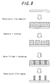
- FIG. 8 is a schematic view explaining respective steps when the partition wall is formed by an additive method in the image display device according to the invention.
- FIG. 9 is a graph explaining a relation between an applied voltage and a reflection density in an estimation of display function of the image display device according to the invention.
- an electric field is applied between opposed substrates, by means of some kind of means, to which particles are sealed.
- a negatively charged particle is attracted toward a portion of the substrate charged positively by means of Coulomb's force and so on, and a positively charged particle is attracted toward a portion of the substrate charged negatively by means of Coulomb's force and so on.
- An image display can be achieved by moving the particles in a reciprocating manner between the opposed substrates.
- the improvement of the stability both in the reciprocating state and the maintaining state by preventing sedimentation and aggregation and the improvement of the decreasing of the drive voltage are an antinomy, and thus it is difficult to realize these improvements at the same time.
- liquid powder means an intermediate material having both of liquid properties and particle properties and exhibiting a self-fluidity without utilizing gas force and liquid force.
- it is a material having an excellent fluidity such that there is no repose angle defining a fluidity of powder.
- a liquid crystal is defined as an intermediate phase between a liquid and a solid, and has a fluidity showing a liquid characteristic and an anisotropy (optical property) showing a solid characteristic (Heibonsha Ltd.: encyclopedia).
- a definition of the particle is a material having a finite mass if it is vanishingly small and receives an attraction of gravity (Maruzen Co., Ltd.: physics subject-book).
- gas-solid fluidized body Even in the particles, there are special states such as gas-solid fluidized body and liquid-solid fluidized body. If a gas is flown from a bottom plate to the particles, an upper force is acted with respect to the particles in response to a gas speed.
- the gas-solid fluidized body means a state that is easily fluidized when the upper force is balanced with the gravity.
- the liquid-solid fluidized body means a state that is fluidized by a liquid.
- the intermediate material having both of fluid properties and solid properties and exhibiting a self-fluidity without utilizing gas force and liquid force can be produced specifically, and this is defined as the liquid powder.
- the liquid powder according to the invention is a material showing the intermediate state having both of liquid properties and particle properties, which is extremely difficult to receive an influence of the gravity showing the particle properties mentioned above and indicates a high fluidity.
- a material can be obtained in an aerosol state i.e. in a dispersion system wherein a solid-like or a liquid-like material is floating in a relatively stable manner as a dispersant in a gas, and thus, in the image display device according to the invention, a solid material is used as a dispersant.
- the liquid powder composed of a solid material stably floating as a dispersant in a gas and exhibiting a high fluidity in an aerosol state is sealed between opposed substrates, at least one of which is transparent.
- the liquid powder can move easily and stably by Coulomb's force and so on driven by a low voltage.
- a repose angle As an index showing a fluidity of the powder, a repose angle is widely used. This means an angle between a free surface of a powder layer and a horizontal surface when, in a gravitational field, the free surface of the powder layer becomes a critical stress state. The fluidity becomes better if this value becomes smaller.
- the value of the repose angle is varied considerably by the measuring method even if the repose angle is measured for the same powder.
- the following three methods are known. 1) Filling method: the powder is filled from an upside to the horizontal surface so as to deposit the powder in a conical shape, and an inclination angle of its inclined plane is measured. 2) Discharging method: the powder filled in a vessel is discharged by gravitation e.g. by opening an outlet arranged at a bottom portion, and an inclination angle of free surface of a remaining layer is measured. 3) Inclination method: the powder is filled in a vessel, its free surface is smoothed in a flat manner, the vessel is inclined and an inclination angle at which the powder arranged on a surface starts to slip is measured.
- the repose angle of the liquid powder according to the present invention is measured according to the measuring methods mentioned above, there occur the following problems.
- the 1) filling method since the liquid powder cannot form a conical shape, its inclination angle cannot be measured.
- the 2) discharging method since the liquid powder cannot form a remaining layer, its inclination angle cannot be measured.
- the 3) inclination method since it is not possible to detect a state at which the liquid powder starts to slip, its inclination angle cannot be measured.
- the repose angle of the liquid powder according to the invention cannot be measured by the measuring methods mentioned above. That is, the liquid powder according to the invention is a material showing such a high fluidity that there is no repose angle.
- An image display in the image display device can be applied to a display method wherein the different liquid powders having two or more colors are moved in a vertical direction with respect to the substrate as shown in FIG. 1 and a display method wherein the liquid powder having one color is moved in a horizontal direction with respect to the substrate as shown in FIG. 2 .
- the former display method is preferred.
- FIGS. 3 a - 3 c are schematic views respectively explaining one embodiment of a structure of the image display device according to the invention.
- the image display device according to (the first aspect of) the invention is constructed as shown in FIG. 3 a by opposed substrates 1 and 2 , a liquid powder 3 between the substrates and a partition wall 4 that is arranged according to need.
- the image display device according to (the second aspect of) the invention is constructed as shown in FIGS. 3 b and 3 c by the opposed substrates 1 and 2 , the liquid powder 3 and a porous spacer 4 .
- At least one of the substrates 1 and 2 is a transparent substrate through which a color of the liquid powder 3 can be observed from outside of the device, and it is preferred to use a material having a high transmission factor of visible light and an excellent heat resistance.
- the image display device whether flexibility is necessary or not is suitably selected in accordance with its use. For example, it is preferred to use a material having flexibility for the use of electronic paper and so on, and it is preferred to use a material having no flexibility for the use of a display of portable device such as mobile phone, PDA, laptop computer and so on.
- the substrate material examples include polymer sheets such as polyethylene terephthalate, polymer sulfone, polyethylene, or polycarbonate, and inorganic sheets such as glass, quartz or so.
- the thickness of the substrate is preferably 2 to 5000 ⁇ m, more preferably 5 to 1000 ⁇ m.
- the thickness is too thin, it becomes difficult to maintain strength and distance uniformity between the substrates, and when the thickness is too thick, vividness and contrast as a display capability degrade, and in particular, flexibility in the case of using for an electronic paper deteriorates.
- An electrode may be arranged on the substrate according to need.
- the liquid powder charged in a predetermined characteristic and having a color is pulled in or rebounds with respect to the substrate by means of an electric field generated by applying an electrostatic latent image on an outer surface of the substrate. Then, the liquid powder aligned in accordance with the electrostatic latent image is observed from outside of the display device through the transparent substrate.
- the electrostatic latent image mentioned above can be generated for example by a method wherein an electrostatic latent image generated in a known electrophotography system using an electrophotography photo-conductor is transferred and formed on the substrate of the image display device according to the invention, or, by a method wherein an electrostatic latent image is directly formed on the substrate by an ion flow.
- the liquid powder charged in a predetermined characteristic and having a color is pulled in or rebounds with respect to the substrate by means of an electric field generated on respective electrodes formed on the substrate by applying an outer voltage thereto. Then, the liquid powder aligned in accordance with the electrostatic latent image is observed from outside of the display device through the transparent substrate.
- the electrode may be formed of electroconductive materials which are transparent and having patter formation capability.
- electroconductive materials indium oxide, metals such as aluminum, electrodonductive polymer such as polyaniline, polypyrrole, polythiophene and so on, formed by for example vacuum vapor deposition, coating and so on.
- the thickness of the electrode may be suitable unless the electroconductivity is absent or any hindrance exists in optical transparency, and it is preferable to be 3 to 1000 nm, more preferable to be 5 to 400 nm.
- the applied outer voltage may be superimposed with a direct current or an alternate current.
- the image display device in order to prevent an unnecessary movement of the liquid powder in a direction parallel to the substrate, it is preferred to form a partition wall bridging the opposed substrates and to construct the display portion by a plurality of display cells.
- a shape of the partition wall is suitably designed in accordance with a size of the liquid powder to be used for the display and is not restricted. However, it is preferred to set a width of the partition wall to 10-1000 ⁇ m more preferably 10-500 ⁇ m and to set a height of the partition wall to 10-5000 ⁇ m more preferably 10-500 ⁇ m.
- a method of forming the partition wall use may be made of a double rib method wherein ribs are formed on the opposed substrates respectively and they are connected with each other and a single rib method wherein a rib is formed on one of the opposed substrates only.
- a double rib method wherein ribs are formed on the opposed substrates respectively and they are connected with each other and a single rib method wherein a rib is formed on one of the opposed substrates only.
- the display cell formed by the partition walls each made of rib has a square shape, a triangular shape, a circular shape as shown in FIG. 4 viewed from a plane surface of the substrate.
- partition wall forming methods include a screen-printing method, a sandblast method, a photo-conductor paste method and an additive method.
- the prepress use may be made of any means even if a predetermined partition wall pattern can be printed, and, for example, use may be made of a plated mesh for securing a high tension, a metal mesh made of a high tension material and so on, a chemical fiber mesh such as a polyester mesh, a tetoron® mesh and so on, and, a combination type mesh wherein polyester mesh is arranged between the prepress and an printing area.
- an attack angle of the squeegee 10-30 degrees more preferably 15-25 degrees, and to set an application pressure of the squeegee to 0.1-10 kg/cm 2 , more preferably 0.5-3 kg/cm 2 .
- polishing agents are controlled to be discharged straight from a nozzle of a sandblast apparatus by adjusting a balance between an air pressure applied to the polishing agents and a discharge amount of the polishing agents.
- polishing agents are controlled to be discharged straight from a nozzle of a sandblast apparatus by adjusting a balance between an air pressure applied to the polishing agents and a discharge amount of the polishing agents.
- polishing agents used for the sandblast use is made of glass beads, talc, calcium carbonate, metal powders and so on.
- the harden portion of the photosensitive pastes include at least inorganic powder, photosensitive resin, photo-initiator and further consist of solvent, resin and additives.
- the pastes for the partition wall include at least inorganic powder and resin, and consist of solvent, additives and so on.
- the inorganic powder use is made of ceramic powder, glass powder or a combination of one or more kinds of them.
- Typical ceramic powder includes ceramic oxides such as ZrO 2 , Al 2 O 3 , CuO, MgO, TiO 2 , ZnO and so on, and ceramic non-oxides such as SiC, AlN, Si 3 O 4 and so on.
- Typical glass powder includes a substance obtained by melting raw materials having SiO 2 , Al 2 O 3 , B 2 O 3 , Bi 2 O 3 , ZnO and so on, and cooling and grinding the melted raw materials.
- a glass transition point Tg is 300-500° C. In this glass transition temperature range, since the firing step can be performed at a relatively low temperature, there is a merit that a resin damage is small.
- Span By setting a value of Span to not more than 8, it is possible make a size of the inorganic powder in the pastes even. Therefore, if the processes of application to hardening for the pastes are repeated to make a lamination, it is possible to form accurately the partition wall.
- the average particle size d(0.5) of the inorganic powder in the pastes is 0.1-20 ⁇ m more preferably 0.3-10 ⁇ m. By doing so, it is also possible to form accurately the partition wall if the above processes are repeated to make a lamination.
- the particle size distribution and the particle size mentioned above can be measured by means of a laser diffraction/scattering method.
- a laser light is incident upon the particles to be measured, a light intensity distribution pattern due to a diffraction/scattering light occurs spatially.
- This light intensity distribution pattern corresponds to the particle size, and thus it is possible to measure the particle size and the particle size distribution.
- the particle size and the particle size distribution are obtained by a volume standard distribution.
- the particle size and the particle size distribution can be measured by means of a measuring apparatus Mastersizer 2000 (Malvern Instruments Ltd.) wherein the particles setting in a nitrogen gas flow are calculated by an installed analysis software (which is based on a volume standard distribution due to Mie's theory).
- the resin included in the pastes for the partition wall can include the inorganic powder mentioned above if a predetermined partition wall can be formed.
- Typical examples of such a resin are thermoplastic resin, heat-hardening resin, and reactive resin.
- a resin having a high molecular weight and a high glass transition point Tg it is preferred to use resins of acrylic-series, styrene-series, epoxy-series, urethane-series, polyester-series, and urea-series and it is especially preferred to use the resins of acrylic-series, epoxy-series, urethane-series, and polyester-series.
- the solvent added in the pastes for the partition wall use is made of any solvent if it can dissolve the inorganic powder and the resin mentioned above.
- Typical examples of such a solvent are aromatic solvents such as ester phthalate, toluene, xylene, benzene; alcoholic solvents such as oxy-alcohol, hexanol, octanol; and ester solvents such as ester acetate and so on. Normally, 0.1-50 weight parts of the solvent is added to the inorganic powder.
- the paste materials mentioned above are dispersed and mixed at a predetermined composition by means of kneader, agitator, or three rollers. If taking into consideration of workability, it is preferred to set a viscosity to 500-300000 cps (500-300000 mPas).
- the porous spacer is arranged between the opposed substrates and the liquid powder is filled in a space between the opposed substrates.
- the porous spacer means a sheet wherein a plurality of holes are opened. It is preferred to use an elastic material as the porous spacer, and for example use may be made of polyurethane, polyester, polyethylene, silicone, natural rubber, synthetic rubber and so on. Moreover, typical method of forming the holes are mechanical methods such as punching and so on; chemical methods such as etching for photosensitive sheet and so on; and optical methods such as laser working and so on.
- a pore size at a display side and a pore size at a none display side for example, in such a manner that (pore size at display side)/(pore size at none display side) is larger than 1.1 preferably in a range of 1.2-3.
- the reason for improving a durability is not certain, but it is estimated as follows. That is, since an angle is added to a surface of the holes, the liquid powder clashes to a cross section (side surface) in the case of a repeated movement even if the liquid powders with antipolarity with each other are agglutinated. Therefore, the agglutinated liquid powders with antipolarity are scattered and thus its durability is improved.
- a thickness of the porous spacer is suitable to set to 5-500 ⁇ m preferably 5-100 ⁇ m. By doing so, it is possible to obtain a merit on its property of low voltage drive and also a merit on manufacturing process of excellent spacer arrangement.
- a hot melt adhesive is arranged on an outer portion of the porous spacer.
- an open rate at a display side of the porous spacer is suitable to set to 40-95% preferably 50-85%. If the open rate is smaller than that range, actual display area becomes small. On the other hand, if the open rate is larger than that range, the actual display area becomes large, but a strength of the porous spacer itself fails. Therefore, it is difficult to maintain an interval between the substrates in a precise manner.
- the liquid powder is an intermediate material having both of liquid properties and particle properties an exhibiting a self-fluidity without utilizing gas force and liquid force.
- the liquid powder becomes particularly an aerosol state, and thus, in the image display device according to the invention, it is utilized under such a condition that a solid material is floated in a gas as a dispersant in a relatively stable manner.
- an apparent volume in a maximum floating state is two times or more than that in none floating state, more preferably 2.5 times or more than that in none floating state, and most preferably three times or more than that in none floating state.
- an upper limit is not defined, but it is preferred that an apparent volume is 12 times or smaller than that in none floating state.
- the apparent volume in the maximum floating state is smaller than two times, a display controlling becomes difficult. On the other hand, if the apparent volume in the maximum floating state is larger than 12 times, a handling inconvenience during a liquid powder filling operation into the device such as a particle over-scattering occurs.
- the apparent volume in the maximum floating state is measured as follows. That is, it is measured by filling the liquid powder in a transparent closed vessel through which the liquid powder is seen; vibrating or dropping the vessel itself to obtain a maximum floating state; and measuring an apparent volume at that time from outside of the vessel.
- the liquid powder having a volume 1 ⁇ 5of the vessel is filled as the liquid powder in a vessel with a polypropylene cap having a diameter (inner diameter) of 6 cm and a height of 10 cm (product name I-boy® produced by As-one Co., Ltd.), the vessel is set in the vibrator, and a vibration wherein a distance of 6 cm is repeated at a speed of 3 reciprocating/sec. is performed for 3 hours.
- the apparent volume in the maximum floating state is obtained from an apparent volume just after a vibration stop.
- a time change of the apparent volume of the liquid powder satisfies the floating formula: V 10 /V 5 >0.8; here, V 5 indicates the apparent volume (cm 3 ) of the liquid powder after 5 minutes from the maximum floating state; and V 10 indicates the apparent volume (cm 3 ) of the liquid powder after 10 minutes from the maximum floating state.
- V 10 /V 5 of the apparent volume of the liquid powder it is preferred to set the time change V 10 /V 5 of the apparent volume of the liquid powder to larger than 0.85, more preferably larger than 0.9, most preferably larger than 0.95. If the time change V 10 /V 5 is not larger than 0.8, the liquid powder is substantially equal to normal particles, and thus it is not possible to maintain a high speed response and durability according to the invention.
- the average particle size d(0.5) of the particle materials constituting the liquid powder is 0.1-20 ⁇ m, more preferably 0.5-15 ⁇ m, most preferably 0.9-8 ⁇ m. If the average particle size d(0.5) is less than 0.1 ⁇ m, a display controlling becomes difficult. On the other hand, if the average particle size d(0.5) is larger than 20 ⁇ m, a display is possible, but opacifying power is decreased and thus a thin shape device is difficult.
- the average particle size d(0.5) of the particle materials constituting the liquid powder is equal to d(0.5) in the following particle size distribution Span.
- the particle size distribution Span of the particle materials constituting the liquid powder is set to not more than 5, the particle size becomes even and it is possible to perform an even liquid powder movement.
- the particle size distribution and the particle size mentioned above can be measured by means of a laser diffraction/scattering method.
- a laser light is incident upon the particles to be measured, a light intensity distribution pattern due to a diffraction/scattering light occurs spatially.
- This light intensity distribution pattern corresponds to the particle size, and thus it is possible to measure the particle size and the particle size distribution.
- the particle size and the particle size distribution are obtained by a volume standard distribution.
- the particle size and the particle size distribution can be measured by means of a measuring apparatus Mastersizer 2000 (Malvern Instruments Ltd.) wherein the particles setting in a nitrogen gas flow are calculated by an installed analysis software (which is based on a volume standard distribution due to Mie's theory).
- the liquid powder may be formed by mixing necessary resin, charge control agent, coloring agent, additive and so on and grinding them, or, by polymerizing from monomer, or, by coating a particle with resin, charge control agent, coloring agent, and additive and so on.
- Typical examples of the resin include urethane resin, acrylic resin, polyester resin, acryl urethane resin, silicone resin, nylon resin, epoxy resin, styrene resin, butyral resin, vinylidene chloride resin, melamine resin, phenolic resin, fluorocarbon polymers, and it is possible to combine two or more resins.
- urethane resin acrylic resin, polyester resin, acryl urethane resin, silicone resin, nylon resin, epoxy resin, styrene resin, butyral resin, vinylidene chloride resin, melamine resin, phenolic resin, fluorocarbon polymers, and it is possible to combine two or more resins.
- acryl urethane resin acryl urethane silicone resin, acryl urethane fluorocarbon polymers, urethane resin, fluorocarbon polymers.
- Examples of the electric charge control agent include, positive charge control agent include the fourth grade ammonium salt compound, nigrosine dye, triphenylmethane compound, imidazole derivatives, and so on, and negative charge control agent such as metal containing azo dye, salicylic acid metal complex, nitroimidazole derivative and so on.
- a coloring agent various kinds of basic or acidic dye may be employable. Examples include Nigrosine, Methylene Blue, quinoline yellow, rose bengal and do on.
- inorganic additives examples include titanium oxide, Chinese white, zinc sulfide, antimonial oxide, calcium carbonate, zinc white, talc, silica, calcium silicate, alumina white, cadmium yellow, cadmium red, cadmium orange, titanium yellow, iron blue, ultramarine blue, cobalt blue, cobalt green, cobalt violet, ferric oxide, carbon black, copper powder, aluminum powder and so on.
- the liquid powder exhibiting an aerosol state cannot be obtained.
- the regular method of forming the liquid powder exhibiting an aerosol state is not defined, but the following method is preferably used.
- inorganic fine particles having an average particle size of 20-100 nm preferably 20-80 nm are preferably fixed on a surface of materials constituting the liquid powder. Moreover, it is preferred to treat the inorganic fine particles by a silicone oil.
- the inorganic fine particles use may be made of silicon dioxide (silica), zinc oxide, aluminum oxide, magnesium oxide, cerium oxide, ferric oxide, copper oxide and so on.
- a method of coating is important.
- the water absorbing rate of the resin constituting the liquid powder sealed between the substrates is not more than 3 wt % especially not more than 2 wt %.
- a measurement of the water absorbing rate is performed according to ASTM-D570 and a measuring condition is 23° C. for 24 hours.
- the solvent insoluble rate is less than 50%, a bleed is generated on a surface of the particle material constituting the liquid powder when maintaining for a long time. In this case, it affects an adhesion power with the liquid powder and prevent a movement of the liquid powder. Therefore, there is a case such that it affects a durability of the image display.
- fluoroplastic such as methyl ethyl ketone and so on, polyamide resin such as methanol and so on, acrylic urethane resin such as methyl ethyl ketone, toluene and so on, melamine resin such as acetone, isopropanol and so on, silicone resin such as toluene and so on.
- an occupied volume (volume occupied rate) of the liquid powder it is preferred to control an occupied volume (volume occupied rate) of the liquid powder to 10-80 vol %, more preferably 10-65 vol %, most preferably 10-55 vol % of a space between the opposed substrates.
- a clear image display is not performed.
- the volume occupied rate is larger than 80 vol %, the liquid powder is difficult to move.
- a gas in a gap surrounding the liquid powder between the substrates it is important to control a gas in a gap surrounding the liquid powder between the substrates, and a suitable gas control contributes an improvement of a display stability. Specifically, it is important to control a humidity of the gap gas to not more than 60% RH at 25° C., preferably not more than 50% RH, more preferably not more than 35% RH.
- the above gap means a gas portion surrounding the liquid powder obtained by substituting an occupied portion of the liquid powder 3 , an occupied portion of the partition wall 4 and a seal portion of the device from the space between the opposed substrates 1 and 2 .
- a kind of the gap gas is not limited if it has the humidity mentioned above, but it is preferred to use dry air, dry nitrogen gas, dry helium gas, dry carbon dioxide gas, dry methane gas and so on.
- the liquid powder In order to obtain the liquid powder exhibiting an aerosol state, it is difficult to use a normal filling method for filling the liquid powder in the display device. In this case, it is preferred to use an electrostatic plating apparatus and to adhere the liquid powder to the substrate by force so as to perform an easy handling. In addition, the liquid powder may be adhered to one substrates or may be adhered to both of the substrates, and then the substrates are connected.
- the image display device is applicable to the image display unit for mobile equipment such as notebook personal computers, PDAs, cellular phones and so on; to the electric paper for electric book, electric newspaper and so on; to the bulletin boards such as signboards, posters, blackboards and so on; to the rewritable paper substituted for a paper of copy machine, printer and so on; and to the image display unit for electric calculator, home electric application products, auto supplies and so on.
- mobile equipment such as notebook personal computers, PDAs, cellular phones and so on
- the electric paper for electric book, electric newspaper and so on to the bulletin boards such as signboards, posters, blackboards and so on
- to the rewritable paper substituted for a paper of copy machine, printer and so on and to the image display unit for electric calculator, home electric application products, auto supplies and so on.
- the particle size and the particle size distribution were measured by means of a measuring apparatus Mastersizer 2000 (Malvern Instruments Ltd.) wherein the particles setting therein are calculated by an installed analysis software (which is based on a volume standard distribution due to Mie's theory) on the basis of the following formula.
- Span ( d (0.9) ⁇ d (0.1))/ d (0.5);
- d(0.5) means a value of the particle size expressed by ⁇ m wherein an amount of the particle material constituting the liquid powder having the particle size larger than this value is 50% and an amount of the particle material constituting the liquid powder having the particle size expressed by ⁇ m wherein an amount of the particle material constituting the liquid powder having a particle size smaller than this value is 10%
- d(0.9) means a value of the particle size expressed by ⁇ m wherein an amount of the particle material constituting the liquid powder having the particle size smaller than this value is 90%).
- the average particle size ( ⁇ m) is the above d(0.5).
- the apparent volume of the liquid powder after 5 minutes from the maximum floating state V 5 (cm 3 ) and the apparent volume of the liquid powder after 10 minutes from the maximum floating state V 10 (cm 3 ) were measured.
- Respective powders were set in Powder Test PT-R (Hosokawa Micron Co., Ltd.), and the repose angle was measured.
- the voltage applied to display device was increased, and the voltage, at which the display becomes capable by the movement of the liquid powder or the powder, was measured as a minimum drive voltage. Specifically, as shown in FIG. 9 , a threshold voltage was defined as the minimum drive voltage.
- the estimation of the display function was performed in such a manner that contrast ratios at initial point, after 20000 times (first aspect of the invention) or 10000 times (second aspect of the invention), and after 5 days left, were measured.
- the contrast ratio was defined by reflection density at black display/reflection density at white (or yellow) display.
- a maintaining rate was defined as a ration of the contrast ratios after 20000 times, 10000 times or 5 days with respect to the initial contrast ratio.
- the colony (agglutination) is generated or not.
- the response speed was measured from the output value deviation by using photomultiplier.
- liquid powder X liquid powder Y
- liquid powder Y liquid powder Y
- the liquid powder X was produced as follows. At first, methyl methacrylate monomer, TiO 2 (20 phr), charge control agent bontron E89 (Orient Chemical Industries, Ltd.: 5 phr), initiator AIBN (0.5 phr) were suspended and polymerized. After that, particle sizes of the polymerized particles were graded by using a grading device. Then, by using hybridizer (Nara Machinery Co., Ltd.), the polymerized particles, external additive A (silica H2000, Wacker Ltd.) and external additive B (silica SS20, Japan Silica Ltd.) were set therein and treated at 4800 rpm for 5 minuets, so that the external additives were fixed on a surface of the polymerized particles to obtain the liquid powder.
- the liquid powder Y was produced as follows. At first, styrene monomer, azo compounds (5 phr), charge control agent bontron N07 (Orient Chemical Industries, Ltd.: 5 phr), initiator AIBN (0.5 phr) were suspended and polymerized. After that, particle sizes of the polymerized particles were graded by using a grading device. Then, by using hybridizer (Nara Machinery Co., Ltd.), the polymerized particles, external additive C (silica H2050, Wacker Ltd.) and external additive B (silica SS20, Japan Silica Ltd.) were set therein and treated at 4800 rpm for 5 minuets, so that the external additives were fixed on a surface of the polymerized particles to obtain the liquid powder.
- the solid state properties of the liquid powder X and the liquid powder Y i.e. the above mentioned (1) average particle size and particle size distribution of the liquid powder, (2) ratio of apparent volume at maximum floating state of the liquid powder and apparent volume at none floating state, (3) time change of the apparent volume of the liquid powder (V 10 /V 5 ), (4) solvent insoluble rate of the liquid powder and (5) repose angle of the liquid powder and the powder were shown in table 1.
- a rib having a height of 250 ⁇ m was produced to form a partition wall having a stripe shape and a single lever construction.
- the production of the rib was performed as follows.
- a glass powder was prepared by melting, cooling and grinding a mixture of SiO 2 , Al 2 O 3 , B 2 O 3 , Bi 2 O 3 , and ZnO.
- a resin epoxy resin having heat hardening property was prepared. Then, the glass powder and the epoxy resin were mixed with a solvent and controlled to be a viscosity of 15000 cps, so that a paste was produced.
- the paste was applied on a substrate and heated at 150° C. to be hardened.
- a thickness (corresponding to a height of the partition wall) was controlled to be 200 ⁇ m.
- a dry photo-resist was adhered.
- an exposing step and an etching step were performed so as to form a mask by which a partition wall pattern having a line of 50 ⁇ m, a space of 200 ⁇ m and a pitch of 250 ⁇ m can be formed.
- the liquid powder X was tentatively adhered to the glass substrate on which the indium oxide electrode is arranged by means of the electrostatic coating machine, and the liquid powder Y was tentatively adhered to another glass substrate. Then, the glass substrates were opposed with a spacing of 120 ⁇ m by using the spacer, and a periphery of the glass substrate is connected by means of epoxy adhesive agent, so that the display device, in which the liquid powder is sealed, was produced.
- the mixing ratio of the liquid powder X and the liquid powder Y was controlled to be even, and the filling rate of the liquid powder between the glass substrates was controlled to be 30 vol % as the volume occupied rate.
- the gas surrounding the liquid powder in the gap between the substrates was an air having a relative humidity of 35% RH.
- the display device was produced in the same manner as that of the example 1, except that main materials of the liquid powder X and the liquid powder Y are urethane (in the liquid powder Y, it was used together with carbon).
- the display device was produced in the same manner as that of the example 1, except that an addition amount of the initiator AIBN of the liquid powder X and the liquid powder Y are changed to 0.1 phr.
- the display device was produced in the same manner as that of the example 1, except that the grading after suspending and polymerizing operation of the liquid powder X and the liquid powder Y is not performed.
- the display device was produced in the same manner as that of the example 1, except that the humidity of the air surrounding the liquid powder in the gap between the substrates was changed to 80% RH.
- the display device was produced in the same manner as that of the example 1, except that the partition wall was not arranged.
- the solid state properties of the liquid powder X and the liquid powder Y and the estimation results of the display function in the display device were shown in the following Table 1. In this case, since the partition wall was not arranged, the durability was slightly deteriorated.
- the liquid powder X was produced in such a manner that acrylic urethane resin EAU65B (Asia-Kogyo Co., Ltd.) was coated on spherical fine particle of white polymethyl methacrylate MX-500 (Soken Chemical & Engineering Co., Ltd.: average particle size of 5.1 ⁇ m) by using agglomaster MINI (Hosakawa Micron Co., Ltd.).
- the coating by using agglomaster MINI was performed by setting the fine particles of 150 g in a treatment vessel maintained at 80° C., rotating at 600 rpm by using an agitating blade, introducing a compressed air having a temperature of 80° C. from a bottom portion of the treatment vessel and agitating the particles. Then, resin and cross-linking agent were dissolved in methyl ethyl ketone solvent, and then it is sprayed for about 30 minutes by means of a spray nozzle.
- the liquid powder Y was produced in such a manner that fluoro-carbon resin KYNAR 2751 (Elf-Atochem-Japan Co., Ltd.) was coated on spherical fine particles of black polymethyl methacrylate CMX-500 (Soken Chemical & Engineering Co., Ltd.: average particle size of 5.1 ⁇ m) by using agglomastaer MINI (Hosokawa Micron Co., Ltd.).
- the display device was produced in the same manner as that of the example 1, except that the above liquid powders were used.
- the solid state properties of the liquid powder X and the liquid powder Y and the estimation results of the display function in the display device were shown in the following Table 2.
- the display device was produced in the same manner as that of the example 7, except that, in the liquid powder X, nylon resin Torejin EF300 (Teikoku Chemical Co., Ltd,) was coated.
- the liquid powder X was produced in such a manner that fluoro-carbon resin KYNAR 2751 (Elf-Atochem-Japan Co., Ltd.) was coated on spherical fine particles of white styrene SX-500 (Soken Chemical & Engineering Co., Ltd.: average particle size of 5.0 ⁇ m) by using CRUX system (Hosokawa Micron Co., Ltd.).
- the coating by using CRUX system was performed by dispersing fine particle: 200 g, coating resin: 10 g and cross-linking agent: 1 g in methyl ethyl ketone (boiling point of 79.6° C.): 5 kg to obtain a slurry, and passing the slurry through a tubule having a diameter of 8 mm and a length of 4 m.
- the liquid powder Y was produced in such a manner that acrylic urethane resin EAU65B (Asia-Kogyo Co., Ltd.) was coated on spherical fine particle of black polymethyl methacrylate CSX-500 (Soken Chemical & Engineering Co., Ltd.: average particle size of 5.0 ⁇ m) by using CRUX system (Hosakawa Micron Co., Ltd.).
- the display device was produced in the same manner as that of the example 1, except that the above liquid powders were used.
- the display device was produced in the same manner as that of the example 9, except that, in the liquid powder Y, nylon resin Torejin EF300 (Teikoku Chemical Co., Ltd,) was coated.
- the liquid powder X was produced in such a manner that the surface treatment was performed by agitating spherical fine particle of white polymethyl methacrylate MX-500 (Soken Chemical & Engineering Co., Ltd.: average particle size of 5.1 ⁇ m): 100 g and dropping hexamethldisilazane: 2 g therein.
- white polymethyl methacrylate MX-500 Soken Chemical & Engineering Co., Ltd.: average particle size of 5.1 ⁇ m
- the liquid powder Y was produced in such a manner that negatively chargeable charge control agent bontron E84 (Orient Chemical Industries Ltd.): 5 parts by weight and carbon black #85 (Degussa Japan Co., Ltd.): 7 parts by weight were mixed with styrene resin MW-1 (TOYO-STYRENE Co., Ltd.), and it was ground and graded.
- negatively chargeable charge control agent bontron E84 Orient Chemical Industries Ltd.
- carbon black #85 Degussa Japan Co., Ltd.
- styrene resin MW-1 TOYO-STYRENE Co., Ltd.
- the display device was produced in the same manner as that of the example 1, except that the above liquid powders were used.
- the display device was produced in the same manner as that of the example 11, except that, in the liquid powder X, spherical fine particles of white styrene SX-500 (Soken Chemical & Engineering Co., Ltd.: average particle size of 5.0 ⁇ m) was used
- the display device was produced in the same manner as that of the example 1, except that, in the manufactures of the liquid powder X and the liquid powder Y, a process condition of the hybridizer was changed to 4800 rpm for 1 minute.
- the display device was produced in the same manner as that of the example 1, except that, in the manufactures of the liquid powder X and the liquid powder Y, a process condition of the hybridizer was changed to 4800 rpm for 30 minutes.
- the display device was produced in the same manner as that of the example 1, except that, instead of the liquid powder X and the liquid powder Y, use was made of commercially available toner for electrophotography.
- the solid state properties of the commercially available toner for electrophotography and the estimation results of the display function in the display device were shown in the following Table 3.
- Example 9 Liquid Main material MX-500 MX-500 SX-500 powder X Coating resin material EAU65B EF300 KYNAR-2751 Processing agent — — — Coating process state AGLOMASTER AGLOMASTER — MINI MINI — — CRUX-system (Solid state properties of liquid powder) Particle size ( ⁇ m) 5.1 5.1 5.0 Distribution of particle size 0.7 0.7 0.6 Span V max /V 0 3.1 3.0 2.9 V 10 /V 5 0.92 0.92 0.90 Repose angle (°) measurement measurement measurement incapable incapable incapable incapable Solvent insoluble rate (%) 95 95 92 Liquid Main material CMX-500 CMX-500 CSX-500 powder Y Coating resin material KYNAR-2751 KYNAR-2751 EAU65B Processing agent — — — Charge control agent — — — Coating process state AGLOMASTER AGLOMASTER — MINI MINI — — CRUX-system (Solid state properties of liquid powder
- Example 3 Liquid (Material of liquid powder) powder X Main material MMA monomer MMA monomer commercially available toner (yellow) TiO 2 TiO 2 Initiator (phr) AIBN(0.5) AIBN(0.5) — Charge control agent bontron E89 bontron E89 — Material of external additive A silica H2000/4 silica H2000/4 — Diameter (nm) 20 20 — Material of external additive B silica SS20 silica SS20 — Diameter (nm) 25 25 — External additive adhesion state: hybridizer hybridizer — processing time of hybridizer 1 30 — (min.) (Solid state properties of liquid powder) Particle size ( ⁇ m) 4.7 4.9 7.2 Distribution of particle size 2.2 1.8 1.8 Span V max /V 0 1.2 1.2 1.2 V 10 /V 5 0.69 0.58 0.68 Repose angle (°) measurement measurement 30 incapable incapable Solvent insoluble rate (%) 91 92
- liquid powder X liquid powder Y
- liquid powder Y liquid powder Y
- the liquid powder X was produced as follows. At first, methyl methacrylate monomer, TiO 2 (20 phr), charge control agent bontron E89 (Orient Chemical Industries, Ltd.: 5 phr), initiator AIBN (0.5 phr) were suspended and polymerized. After that, particle sizes of the polymerized particles were aligned by using an alignment device. Then, by using hybridizer (Nara Machinery Co., Ltd.), the polymerized particles, external additive A (silica H2000, Wacker Ltd.) and external additive B (silica SS20, Japan Silica Ltd.) were set therein and treated at 4800 rpm for 5 minuets, so that the external additives were fixed on a surface of the polymerized particles to obtain the liquid powder.
- the liquid powder Y was produced as follows. At first, styrene monomer, azo compounds (5 phr), charge control agent bontron N07 (Orient Chemical Industries, Ltd.: 5 phr), initiator AIBN (0.5 phr) were suspended and polymerized. After that, particle sizes of the polymerized particles were aligned by using an alignment device. Then, by using hybridizer (Nara Machinery Co., Ltd.), the polymerized particles, external additive C (silica H2050, Wacker Ltd.) and external additive B (silica SS20, Japan Silica Ltd.) were set therein and treated at 4800 rpm for 5 minuets, so that the external additives were fixed on a surface of the polymerized particles to obtain the liquid powder.
- the solid state properties of the liquid powder X and the liquid powder Y i.e. the above mentioned (1) average particle size and particle size distribution of the particle materials constituting the liquid powder, (2) ratio of apparent volume at maximum floating state of the liquid powder and apparent volume at none floating state, (3) time change of the apparent volume of the liquid powder (V 10 /V 5 ), and (4) solvent insoluble rate of the liquid powder were shown in the following Table 4.
- a porous spacer was prepared. Then, the porous sheet was formed by preparing polyurethane sheet having a thickness of 200 ⁇ m, and punching mechanically the sheet to open a hole in such a manner that a hole diameter at the display side is 6 mm and a hole diameter at the none-display side is 5 mm and further the open rate becomes 80%.
- the hot melt adhesives were arranged at a peripheral portion of the porous sheet.
- the porous spacer On a glass substrate to which indium oxide having a thickness of about 500 ⁇ was arranged, the porous spacer was arranged. Then, the porous spacer was pressed with pressure by means of an application device heated at a temperature at which the hot melt adhesives were melted, and the porous spacer was connected to the glass substrate.
- the liquid powder X was tentatively adhered to the glass substrate on which the porous spacer is arranged by means of the electrostatic coating machine, and the liquid powder Y was tentatively adhered thereto. Further, the liquid powders were removed at a portion other than the hole for the porous spacer. Then, another glass substrate to which indium oxide electrode is arranged was opposed to the glass substrate, and a periphery of the glass substrate is connected by means of epoxy adhesive agent, so that the display device, in which the liquid powder is sealed, was produced.
- the mixing ratio of the liquid powder X and the liquid powder Y was controlled to be even, and the filling rate of the liquid powder between the glass substrates was controlled to be 25 vol % as the volume occupied rate.
- the gas surrounding the liquid powder in the gap between the substrates was an air having a relative humidity of 35% RH.
- the display device was produced in the same manner as that of the example 21, except that an addition amount of the initiator AIBN of the liquid powder X and the liquid powder Y are changed to 0.1 phr.
- the display device was produced in the same manner as that of the example 21, except that the grading after suspending and polymerizing operation of the liquid powder X and the liquid powder Y is not performed.
- the display device was produced in the same manner as that of the example 21, except that the humidity of the air surrounding the liquid powder in the gap between the substrates was changed to 80% RH.
- the display device was produced in the same manner as that of the example 21, except that, in the manufactures of the liquid powder X and the liquid powder Y, a process condition of the hybridizer was changed to 4000 rpm for 2 minutes.
- the display device was produced in the same manner as that of the example 21, except that, in the manufactures of the liquid powder X and the liquid powder Y, a process condition of the hybridizer was changed to 4000 rpm for 25 minutes.
- the display device was produced in the same manner as that of the example 21, except that the hole diameter at the none-display side was also 6 mm as is the same as the display side.
- the solid state properties of the liquid powder X and the liquid powder Y and the estimation results of the display function in the display device were shown in the following Table 5. In this case, since the hole diameters at the display side and at the none-display side were even, the response speed slightly became slow.
- the display device was produced in the same manner as that of the example 21, except that the porous spacer was not used.
- the solid state properties of the liquid powder X and the liquid powder Y and the estimation results of the display function in the display device were shown in the following Table 5. In this case, since the colony (agglutination) of the liquid powder was generated, the durability was deteriorated.
- the display device was produced in the same manner as that of the example 21, except that the porous spacer was not used and, instead of the liquid powder X and the liquid powder Y, use was made of commercially available toner for electrophotography.
- the solid state properties of the commercially available toner for electrophotography and the estimation results of the display function in the display device were shown in the following Table 5. From the results, it was understood that the liquid powder state was deteriorated, the drive voltage became high, the durability was deteriorated and the response speed became slow.
- Example 22 Liquid (Material of liquid powder) powder X Main material MMA monomer MMA monomer MMA monomer TiO 2 TiO 2 TiO 2 Initiator (phr) AIBN(0.4) AIBN(0.1) AIBN(0.4) Charge control agent bontron 89 bontron 89 bontron 89 Material of external additive A silica H2000 silica H2000 silica H2000 Diameter (nm) 20 20 20 Material of external additive B silica SS20 silica SS20 silica SS20 Diameter (nm) 25 25 25 25 25 25 25 25 25 25 25 25 25 25 25 25 25 25 25 25 25 25 25 25 25 25 25 25 25 25 25 25 25 25 25 25 25 25 25 25 25 25 25 25 25 25 25 25 25 25 25 25 25 25 25 25 25 25 25 25 25 25 25 25 25 25 25 25 25 25 25 25 25 25 25 25 25 25 25 25 25 25 25 25 25 25 25 25 25 25 25 25 25 25 25 25 25 25 25 25 25 25 25 25 25 25 25 25 25 25 25 25 25 25 25 25 External additive
- Example 27 Liquid (Material of liquid powder) powder X Main material MMA monomer urethane TiO 2 TiO 2 Initiator (phr) AIBN(0.4) AIBN(0.4) Charge control agent bontron 89 bontron 89 Material of external additive A silica H2000 silica H2000 Diameter (nm) 20 20 Material of external additive B silica SS20 silica SS20 Diameter (nm) 25 25 External additive adhesion state: processing time of hybridizer (min.) 25 6 (Solid state properties of liquid powder) Particle size ( ⁇ m) 4.8 3.2 Distribution of particle size Span 1.7 1.5 V max /V 0 1.7 3.2 V 10 /V 5 0.7 0.90 Solvent insoluble rate (%) 92 92 Liquid (Material of liquid powder) powder Y Main material styrene styrene monomer monomer azo-series azo-series compound compound Initiator (phr) AIBN(0.4) AIBN(
- a liquid powder composed of a solid material stably floating as a dispersant in a gas and exhibiting a high fluidity in an aerosol state is sealed between opposed substrates and the liquid powder is moved, it is possible to obtain an image display device and method which can realize rapid response and also which can achieve inexpensive and stable construction and further decrease the drive voltage.
- a porous spacer is arranged between opposed substrates, a liquid powder composed of a solid material stably floating as a dispersant in gas and exhibiting a high fluidity in an aerosol state is sealed, and the liquid powder is moved, it is possible to obtain an image display device which can achieve inexpensive construction, improve durability and decrease a drive voltage.
Landscapes
- Physics & Mathematics (AREA)
- Nonlinear Science (AREA)
- General Physics & Mathematics (AREA)
- Optics & Photonics (AREA)
- Health & Medical Sciences (AREA)
- Life Sciences & Earth Sciences (AREA)
- Chemical & Material Sciences (AREA)
- Chemical Kinetics & Catalysis (AREA)
- Electrochemistry (AREA)
- Molecular Biology (AREA)
- Electrochromic Elements, Electrophoresis, Or Variable Reflection Or Absorption Elements (AREA)
- Adhesives Or Adhesive Processes (AREA)
Applications Claiming Priority (5)
| Application Number | Priority Date | Filing Date | Title |
|---|---|---|---|
| JP2002060760 | 2002-03-06 | ||
| JP200260760 | 2002-03-06 | ||
| JP2002133171 | 2002-05-08 | ||
| JP2002133171 | 2002-05-08 | ||
| PCT/JP2003/002645 WO2003075087A1 (fr) | 2002-03-06 | 2003-03-06 | Appareil et procede d'affichage d'images |
Publications (2)
| Publication Number | Publication Date |
|---|---|
| US20060033849A1 US20060033849A1 (en) | 2006-02-16 |
| US7321459B2 true US7321459B2 (en) | 2008-01-22 |
Family
ID=27790990
Family Applications (1)
| Application Number | Title | Priority Date | Filing Date |
|---|---|---|---|
| US10/506,533 Expired - Fee Related US7321459B2 (en) | 2002-03-06 | 2003-03-06 | Image display device and method |
Country Status (8)
| Country | Link |
|---|---|
| US (1) | US7321459B2 (ja) |
| EP (1) | EP1482354B1 (ja) |
| JP (1) | JP4202266B2 (ja) |
| KR (1) | KR100639546B1 (ja) |
| CN (1) | CN100339757C (ja) |
| AU (1) | AU2003213409A1 (ja) |
| DE (1) | DE60320640T2 (ja) |
| WO (1) | WO2003075087A1 (ja) |
Cited By (203)
| Publication number | Priority date | Publication date | Assignee | Title |
|---|---|---|---|---|
| US20060087489A1 (en) * | 2002-07-17 | 2006-04-27 | Ryou Sakurai | Image display |
| US20070035808A1 (en) * | 2001-07-09 | 2007-02-15 | E Ink Corporation | Electro-optic display and materials for use therein |
| US20070153361A1 (en) * | 2002-06-10 | 2007-07-05 | E Ink Corporation | Components and testing methods for use in the production of electro-optic displays |
| US20070211331A1 (en) * | 2006-03-08 | 2007-09-13 | E Ink Corporation | Electro-optic displays, and materials and methods for production thereof |
| US20070223079A1 (en) * | 2006-03-22 | 2007-09-27 | E Ink Corporation | Electro-optic media produced using ink jet printing |
| US20070247697A1 (en) * | 2003-11-05 | 2007-10-25 | E Ink Corporation | Electro-optic displays, and materials for use therein |
| US20070286975A1 (en) * | 2003-11-05 | 2007-12-13 | E Ink Corporation | Electro-optic displays, and materials for use therein |
| US20080013156A1 (en) * | 2006-07-13 | 2008-01-17 | E Ink Corporation | Particles for use in electrophoretic displays |
| US20080013155A1 (en) * | 2006-07-11 | 2008-01-17 | E Ink Corporation | Electrophoretic medium and display with improved image stability |
| US20080024429A1 (en) * | 2006-07-25 | 2008-01-31 | E Ink Corporation | Electrophoretic displays using gaseous fluids |
| US20080023332A1 (en) * | 2003-03-25 | 2008-01-31 | E Ink Corporation | Processes for the production of electrophoretic displays |
| US20080030832A1 (en) * | 2006-08-02 | 2008-02-07 | E Ink Corporation | Multi-layer light modulator |
| US20080043318A1 (en) * | 2005-10-18 | 2008-02-21 | E Ink Corporation | Color electro-optic displays, and processes for the production thereof |
| US20080057252A1 (en) * | 2002-06-10 | 2008-03-06 | E Ink Corporation | Components and methods for use in electro-optic displays |
| US20080074730A1 (en) * | 2006-09-22 | 2008-03-27 | E Ink Corporation | Electro-optic display and materials for use therein |
| US20080137176A1 (en) * | 2006-12-07 | 2008-06-12 | E Ink Corporation | Components and methods for use in electro-optic displays |
| US20080174853A1 (en) * | 2007-01-22 | 2008-07-24 | E Ink Corporation | Multi-layer sheet for use in electro-optic displays |
| US20080218839A1 (en) * | 2003-11-05 | 2008-09-11 | E Ink Corporation | Electro-optic displays, and materials for use therein |
| US20080254272A1 (en) * | 2007-01-22 | 2008-10-16 | E Ink Corporation | Multi-layer sheet for use in electro-optic displays |
| US20080266646A1 (en) * | 1995-07-20 | 2008-10-30 | E Ink Corporation | Electrophoretic displays with controlled amounts of pigment |
| US20080266245A1 (en) * | 2001-04-02 | 2008-10-30 | E Ink Corporation | Electrophoretic displays with controlled amounts of pigment |
| US20080291129A1 (en) * | 2007-05-21 | 2008-11-27 | E Ink Corporation | Methods for driving video electro-optic displays |
| US20080309350A1 (en) * | 2006-03-08 | 2008-12-18 | E Ink Corporation | Electro-optic displays, and materials and methods for production thereof |
| US20080316582A1 (en) * | 2006-03-08 | 2008-12-25 | E Ink Corporation | Electro-optic displays, and materials and methods for production thereof |
| US20090004442A1 (en) * | 2007-06-28 | 2009-01-01 | E Ink Corporation | Processes for the production of electro-optic displays, and color filters for use therein |
| US20090000729A1 (en) * | 2007-06-29 | 2009-01-01 | E Ink Corporation | Electro-optic displays, and materials and methods for production thereof |
| US20090009852A1 (en) * | 2001-05-15 | 2009-01-08 | E Ink Corporation | Electrophoretic particles and processes for the production thereof |
| US20090109519A1 (en) * | 2007-03-06 | 2009-04-30 | E Ink Corporation | Materials for use in electrophoretic displays |
| US20090122389A1 (en) * | 2007-11-14 | 2009-05-14 | E Ink Corporation | Electro-optic assemblies, and adhesives and binders for use therein |
| US20090168067A1 (en) * | 2002-06-10 | 2009-07-02 | E Ink Corporation | Components and methods for use in electro-optic displays |
| US20090231661A1 (en) * | 2005-06-23 | 2009-09-17 | E Ink Corporation | Edge seals for, and processes for assembly of, electro-optic displays |
| US20090237776A1 (en) * | 2008-03-21 | 2009-09-24 | E Ink Corporation | Electro-optic displays, and color filters for use therein |
| US7649674B2 (en) | 2002-06-10 | 2010-01-19 | E Ink Corporation | Electro-optic display with edge seal |
| US20100045592A1 (en) * | 1995-07-20 | 2010-02-25 | E Ink Corporation | Dielectrophoretic displays |
| US7679814B2 (en) | 2001-04-02 | 2010-03-16 | E Ink Corporation | Materials for use in electrophoretic displays |
| US20100103502A1 (en) * | 1998-07-08 | 2010-04-29 | E Ink Corporation | Methods for achieving improved color in microencapsulated electrophoretic devices |
| US20100165446A1 (en) * | 2002-06-10 | 2010-07-01 | E Ink Corporation | Components and methods for use in electro-optic displays |
| US20100201651A1 (en) * | 2001-03-13 | 2010-08-12 | E Ink Corporation | Apparatus for displaying drawings |
| US20100225995A1 (en) * | 2009-03-03 | 2010-09-09 | E Ink Corporation | Electro-optic displays, and color filters for use therein |
| US20100265239A1 (en) * | 2002-04-24 | 2010-10-21 | E Ink Corporation | Processes for forming backplanes for electro-optic displays |
| US20100289736A1 (en) * | 2009-02-09 | 2010-11-18 | E Ink Corporation | Electrophoretic particles, and processes for the production thereof |
| US7839564B2 (en) | 2002-09-03 | 2010-11-23 | E Ink Corporation | Components and methods for use in electro-optic displays |
| US20110007381A1 (en) * | 1997-08-28 | 2011-01-13 | E Ink Corporation | Multi-color electrophoretic displays |
| US20110012825A1 (en) * | 2001-05-15 | 2011-01-20 | E Ink Corporation | Electrophoretic particles and processes for the production thereof |
| US20110164307A1 (en) * | 2002-06-10 | 2011-07-07 | E Ink Corporation | Electro-optic displays, and processes for the production thereof |
| US7986450B2 (en) | 2006-09-22 | 2011-07-26 | E Ink Corporation | Electro-optic display and materials for use therein |
| US20110193840A1 (en) * | 1995-07-20 | 2011-08-11 | E Ink Corporation | Methods for driving electrophoretic displays using dielectrophoretic forces |
| US20110193841A1 (en) * | 2002-06-13 | 2011-08-11 | E Ink Corporation | Methods for driving electrophoretic displays using dielectrophoretic forces |
| US8115729B2 (en) | 1999-05-03 | 2012-02-14 | E Ink Corporation | Electrophoretic display element with filler particles |
| US8314784B2 (en) | 2008-04-11 | 2012-11-20 | E Ink Corporation | Methods for driving electro-optic displays |
| US20120293859A1 (en) * | 2010-01-27 | 2012-11-22 | Dai Nippon Printing Co., Ltd. | Method of manufacturing electrophoretic display device |
| US8446664B2 (en) | 2010-04-02 | 2013-05-21 | E Ink Corporation | Electrophoretic media, and materials for use therein |
| US20130278993A1 (en) * | 2010-09-02 | 2013-10-24 | Jason Heikenfeld | Color-mixing bi-primary color systems for displays |
| US8576476B2 (en) | 2010-05-21 | 2013-11-05 | E Ink Corporation | Multi-color electro-optic displays |
| US8576470B2 (en) | 2010-06-02 | 2013-11-05 | E Ink Corporation | Electro-optic displays, and color alters for use therein |
| US8610988B2 (en) | 2006-03-09 | 2013-12-17 | E Ink Corporation | Electro-optic display with edge seal |
| US8654436B1 (en) | 2009-10-30 | 2014-02-18 | E Ink Corporation | Particles for use in electrophoretic displays |
| US8754859B2 (en) | 2009-10-28 | 2014-06-17 | E Ink Corporation | Electro-optic displays with touch sensors and/or tactile feedback |
| US8797634B2 (en) | 2010-11-30 | 2014-08-05 | E Ink Corporation | Multi-color electrophoretic displays |
| US8873129B2 (en) | 2011-04-07 | 2014-10-28 | E Ink Corporation | Tetrachromatic color filter array for reflective display |
| US8902153B2 (en) | 2007-08-03 | 2014-12-02 | E Ink Corporation | Electro-optic displays, and processes for their production |
| US9195111B2 (en) | 2013-02-11 | 2015-11-24 | E Ink Corporation | Patterned electro-optic displays and processes for the production thereof |
| US9230492B2 (en) | 2003-03-31 | 2016-01-05 | E Ink Corporation | Methods for driving electro-optic displays |
| US9238340B2 (en) | 2012-07-27 | 2016-01-19 | E Ink Corporation | Processes for the production of electro-optic displays |
| US9269311B2 (en) | 2001-11-20 | 2016-02-23 | E Ink Corporation | Methods and apparatus for driving electro-optic displays |
| US9412314B2 (en) | 2001-11-20 | 2016-08-09 | E Ink Corporation | Methods for driving electro-optic displays |
| US9436056B2 (en) | 2013-02-06 | 2016-09-06 | E Ink Corporation | Color electro-optic displays |
| US9470950B2 (en) | 2002-06-10 | 2016-10-18 | E Ink Corporation | Electro-optic displays, and processes for the production thereof |
| US9495918B2 (en) | 2013-03-01 | 2016-11-15 | E Ink Corporation | Methods for driving electro-optic displays |
| US9513743B2 (en) | 2012-06-01 | 2016-12-06 | E Ink Corporation | Methods for driving electro-optic displays |
| US9529240B2 (en) | 2014-01-17 | 2016-12-27 | E Ink Corporation | Controlled polymeric material conductivity for use in a two-phase electrode layer |
| US9530363B2 (en) | 2001-11-20 | 2016-12-27 | E Ink Corporation | Methods and apparatus for driving electro-optic displays |
| WO2017004113A1 (en) | 2015-06-30 | 2017-01-05 | E Ink Corporation | Multi-layered electrophoretic displays |
| US9564088B2 (en) | 2001-11-20 | 2017-02-07 | E Ink Corporation | Electro-optic displays with reduced remnant voltage |
| US9620048B2 (en) | 2013-07-30 | 2017-04-11 | E Ink Corporation | Methods for driving electro-optic displays |
| US9620066B2 (en) | 2010-02-02 | 2017-04-11 | E Ink Corporation | Method for driving electro-optic displays |
| US9664978B2 (en) | 2002-10-16 | 2017-05-30 | E Ink Corporation | Electrophoretic displays |
| US9671635B2 (en) | 2014-02-07 | 2017-06-06 | E Ink Corporation | Electro-optic display backplane structures with drive components and pixel electrodes on opposed surfaces |
| US9688859B2 (en) | 2014-02-06 | 2017-06-27 | E Ink Corporation | Electrophoretic particles and processes for the production thereof |
| US9697778B2 (en) | 2013-05-14 | 2017-07-04 | E Ink Corporation | Reverse driving pulses in electrophoretic displays |
| US9715155B1 (en) | 2013-01-10 | 2017-07-25 | E Ink Corporation | Electrode structures for electro-optic displays |
| US9721495B2 (en) | 2013-02-27 | 2017-08-01 | E Ink Corporation | Methods for driving electro-optic displays |
| US9726957B2 (en) | 2013-01-10 | 2017-08-08 | E Ink Corporation | Electro-optic display with controlled electrochemical reactions |
| WO2017139323A1 (en) | 2016-02-08 | 2017-08-17 | E Ink Corporation | Methods and apparatus for operating an electro-optic display in white mode |
| US9752034B2 (en) | 2015-11-11 | 2017-09-05 | E Ink Corporation | Functionalized quinacridone pigments |
| US9765015B2 (en) | 2016-01-17 | 2017-09-19 | E Ink California, Llc | Branched polyol additives for electrophoretic media |
| US9777201B2 (en) | 2015-07-23 | 2017-10-03 | E Ink Corporation | Polymer formulations for use with electro-optic media |
| US9779671B2 (en) | 2012-05-31 | 2017-10-03 | E Ink Corporation | Image display medium driving device, image display apparatus, driving program, and computer-readable medium |
| US9835925B1 (en) | 2015-01-08 | 2017-12-05 | E Ink Corporation | Electro-optic displays, and processes for the production thereof |
| US9880646B2 (en) | 2015-02-18 | 2018-01-30 | E Ink Corporation | Addressable electro-optic display |
| US9921451B2 (en) | 2014-09-10 | 2018-03-20 | E Ink Corporation | Colored electrophoretic displays |
| US9953588B1 (en) | 2014-03-25 | 2018-04-24 | E Ink Corporation | Nano-particle based variable transmission devices |
| US10037735B2 (en) | 2012-11-16 | 2018-07-31 | E Ink Corporation | Active matrix display with dual driving modes |
| US10037089B2 (en) | 2015-02-17 | 2018-07-31 | E Ink Corporation | Electromagnetic writing apparatus for electro-optic displays |
| US10040954B2 (en) | 2015-05-28 | 2018-08-07 | E Ink California, Llc | Electrophoretic medium comprising a mixture of charge control agents |
| US10048564B2 (en) | 2003-11-05 | 2018-08-14 | E Ink Corporation | Electro-optic displays, and materials for use therein |
| US10061123B2 (en) | 2016-01-17 | 2018-08-28 | E Ink California, Llc | Surfactants for improving electrophoretic media performance |
| WO2018165509A1 (en) | 2017-03-09 | 2018-09-13 | E Ink Corporation | Drivers providing dc-balanced refresh sequences for color electrophoretic displays |
| US10146261B2 (en) | 2016-08-08 | 2018-12-04 | E Ink Corporation | Wearable apparatus having a flexible electrophoretic display |
| US10163406B2 (en) | 2015-02-04 | 2018-12-25 | E Ink Corporation | Electro-optic displays displaying in dark mode and light mode, and related apparatus and methods |
| US10175550B2 (en) | 2014-11-07 | 2019-01-08 | E Ink Corporation | Applications of electro-optic displays |
| US10174232B2 (en) | 2015-09-30 | 2019-01-08 | E Ink Corporation | Polyurethane adhesive layers for electro-optic assemblies |
| US10190743B2 (en) | 2012-04-20 | 2019-01-29 | E Ink Corporation | Illumination systems for reflective displays |
| US10197883B2 (en) | 2015-01-05 | 2019-02-05 | E Ink Corporation | Electro-optic displays, and methods for driving same |
| US10254620B1 (en) | 2016-03-08 | 2019-04-09 | E Ink Corporation | Encapsulated photoelectrophoretic display |
| US10276109B2 (en) | 2016-03-09 | 2019-04-30 | E Ink Corporation | Method for driving electro-optic displays |
| US10282033B2 (en) | 2012-06-01 | 2019-05-07 | E Ink Corporation | Methods for updating electro-optic displays when drawing or writing on the display |
| WO2019089042A1 (en) | 2017-11-03 | 2019-05-09 | E Ink Corporation | Processes for producing electro-optic displays |
| US10317767B2 (en) | 2014-02-07 | 2019-06-11 | E Ink Corporation | Electro-optic display backplane structure with drive components and pixel electrodes on opposed surfaces |
| US10353266B2 (en) | 2014-09-26 | 2019-07-16 | E Ink Corporation | Color sets for low resolution dithering in reflective color displays |
| WO2019144097A1 (en) | 2018-01-22 | 2019-07-25 | E Ink Corporation | Electro-optic displays, and methods for driving same |
| US10372008B2 (en) | 2011-05-21 | 2019-08-06 | E Ink Corporation | Electro-optic displays |
| US10388233B2 (en) | 2015-08-31 | 2019-08-20 | E Ink Corporation | Devices and techniques for electronically erasing a drawing device |
| US10444592B2 (en) | 2017-03-09 | 2019-10-15 | E Ink Corporation | Methods and systems for transforming RGB image data to a reduced color set for electro-optic displays |
| US10446585B2 (en) | 2014-03-17 | 2019-10-15 | E Ink Corporation | Multi-layer expanding electrode structures for backplane assemblies |
| WO2019209240A1 (en) | 2018-04-23 | 2019-10-31 | E Ink Corporation | Nano-particle based variable transmission devices |
| US10467984B2 (en) | 2017-03-06 | 2019-11-05 | E Ink Corporation | Method for rendering color images |
| WO2019222587A1 (en) | 2018-05-17 | 2019-11-21 | E Ink California, Llc | Piezo electrophoretic display |
| WO2020018508A1 (en) | 2018-07-17 | 2020-01-23 | E Ink California, Llc | Electro-optic displays and driving methods |
| US10545622B2 (en) | 2016-05-20 | 2020-01-28 | E Ink Corporation | Magnetically-responsive display including a recording layer configured for local and global write/erase |
| WO2020033176A1 (en) | 2018-08-07 | 2020-02-13 | E Ink Corporation | Flexible encapsulated electro-optic media |
| US10573222B2 (en) | 2015-01-05 | 2020-02-25 | E Ink Corporation | Electro-optic displays, and methods for driving same |
| US10573257B2 (en) | 2017-05-30 | 2020-02-25 | E Ink Corporation | Electro-optic displays |
| US10585325B2 (en) | 2017-03-09 | 2020-03-10 | E Ink California, Llc | Photo-thermally induced polymerization inhibitors for electrophoretic media |
| US10593272B2 (en) | 2016-03-09 | 2020-03-17 | E Ink Corporation | Drivers providing DC-balanced refresh sequences for color electrophoretic displays |
| WO2020060797A1 (en) | 2018-09-20 | 2020-03-26 | E Ink Corporation | Three-dimensional display apparatuses |
| WO2020092190A1 (en) | 2018-10-30 | 2020-05-07 | E Ink Corporation | Electro-optic medium and writable device incorporating the same |
| US10657869B2 (en) | 2014-09-10 | 2020-05-19 | E Ink Corporation | Methods for driving color electrophoretic displays |
| US10672350B2 (en) | 2012-02-01 | 2020-06-02 | E Ink Corporation | Methods for driving electro-optic displays |
| US10670892B2 (en) | 2016-04-22 | 2020-06-02 | E Ink Corporation | Foldable electro-optic display apparatus |
| WO2020122917A1 (en) | 2018-12-13 | 2020-06-18 | E Ink Corporation | Illumination systems for reflective displays |
| US10726798B2 (en) | 2003-03-31 | 2020-07-28 | E Ink Corporation | Methods for operating electro-optic displays |
| US10802373B1 (en) | 2017-06-26 | 2020-10-13 | E Ink Corporation | Reflective microcells for electrophoretic displays and methods of making the same |
| US10809590B2 (en) | 2017-06-16 | 2020-10-20 | E Ink Corporation | Variable transmission electrophoretic devices |
| US10823373B2 (en) | 2018-12-17 | 2020-11-03 | E Ink Corporation | Light emitting device including variable transmission film to control intensity and pattern |
| US10824042B1 (en) | 2017-10-27 | 2020-11-03 | E Ink Corporation | Electro-optic display and composite materials having low thermal sensitivity for use therein |
| US10832622B2 (en) | 2017-04-04 | 2020-11-10 | E Ink Corporation | Methods for driving electro-optic displays |
| US10852568B2 (en) | 2017-03-03 | 2020-12-01 | E Ink Corporation | Electro-optic displays and driving methods |
| US10962816B2 (en) | 2017-06-16 | 2021-03-30 | E Ink Corporation | Flexible color-changing fibers and fabrics |
| US10983410B2 (en) | 2017-06-16 | 2021-04-20 | E Ink Corporation | Electro-optic media including encapsulated pigments in gelatin binder |
| US11030936B2 (en) | 2012-02-01 | 2021-06-08 | E Ink Corporation | Methods and apparatus for operating an electro-optic display in white mode |
| WO2021133541A1 (en) | 2019-12-23 | 2021-07-01 | E Ink Corporation | Transferable light-transmissive electrode films for electro-optic devices |
| US11062663B2 (en) | 2018-11-30 | 2021-07-13 | E Ink California, Llc | Electro-optic displays and driving methods |
| US11081066B2 (en) | 2018-02-15 | 2021-08-03 | E Ink Corporation | Via placement for slim border electro-optic display backplanes with decreased capacitive coupling between t-wires and pixel electrodes |
| US11079651B2 (en) | 2017-12-15 | 2021-08-03 | E Ink Corporation | Multi-color electro-optic media |
| US11098206B2 (en) | 2015-10-06 | 2021-08-24 | E Ink Corporation | Electrophoretic media including charge control agents comprising quartenary amines and unsaturated polymeric tails |
| US11143930B2 (en) | 2018-06-28 | 2021-10-12 | E Ink Corporation | Driving methods for variable transmission electro-phoretic media |
| US11143929B2 (en) | 2018-03-09 | 2021-10-12 | E Ink Corporation | Reflective electrophoretic displays including photo-luminescent material and color filter arrays |
| US11175561B1 (en) | 2018-04-12 | 2021-11-16 | E Ink Corporation | Electrophoretic display media with network electrodes and methods of making and using the same |
| US11195480B2 (en) | 2013-07-31 | 2021-12-07 | E Ink Corporation | Partial update driving methods for bistable electro-optic displays and display controllers using the same |
| US11237419B2 (en) | 2020-03-05 | 2022-02-01 | E Ink Corporation | Switchable light modulator comprising a polymer wall structure having a mould part and a cast part disposed between first and second substrates |
| US11248122B2 (en) | 2017-12-30 | 2022-02-15 | E Ink Corporation | Pigments for electrophoretic displays |
| US11250794B2 (en) | 2004-07-27 | 2022-02-15 | E Ink Corporation | Methods for driving electrophoretic displays using dielectrophoretic forces |
| US11257445B2 (en) | 2019-11-18 | 2022-02-22 | E Ink Corporation | Methods for driving electro-optic displays |
| US11289036B2 (en) | 2019-11-14 | 2022-03-29 | E Ink Corporation | Methods for driving electro-optic displays |
| US11287718B2 (en) | 2015-08-04 | 2022-03-29 | E Ink Corporation | Reusable display addressable with incident light |
| US11397361B2 (en) | 2015-06-29 | 2022-07-26 | E Ink Corporation | Method for mechanical and electrical connection to display electrodes |
| US11402719B2 (en) | 2018-12-11 | 2022-08-02 | E Ink Corporation | Retroreflective electro-optic displays |
| US11404013B2 (en) | 2017-05-30 | 2022-08-02 | E Ink Corporation | Electro-optic displays with resistors for discharging remnant charges |
| US11422427B2 (en) | 2017-12-19 | 2022-08-23 | E Ink Corporation | Applications of electro-optic displays |
| US11423852B2 (en) | 2017-09-12 | 2022-08-23 | E Ink Corporation | Methods for driving electro-optic displays |
| US11450262B2 (en) | 2020-10-01 | 2022-09-20 | E Ink Corporation | Electro-optic displays, and methods for driving same |
| US11450286B2 (en) | 2015-09-16 | 2022-09-20 | E Ink Corporation | Apparatus and methods for driving displays |
| US11460722B2 (en) | 2019-05-10 | 2022-10-04 | E Ink Corporation | Colored electrophoretic displays |
| US11467466B2 (en) | 2012-04-20 | 2022-10-11 | E Ink Corporation | Illumination systems for reflective displays |
| US11493821B2 (en) | 2018-08-14 | 2022-11-08 | E Ink California, Llc | Piezo electrophoretic display |
| US11520211B2 (en) | 2018-12-17 | 2022-12-06 | E Ink Corporation | Anisotropically conductive moisture barrier films and electro-optic assemblies containing the same |
| US11520179B2 (en) | 2002-09-03 | 2022-12-06 | E Ink Corporation | Method of forming an electrophoretic display having a color filter array |
| US11520210B2 (en) | 2019-09-30 | 2022-12-06 | E Ink Corporation | Electrically-actuated variable transmission film having very low haze and a visible grid in a clear state |
| US11520202B2 (en) | 2020-06-11 | 2022-12-06 | E Ink Corporation | Electro-optic displays, and methods for driving same |
| US11557260B2 (en) | 2020-11-02 | 2023-01-17 | E Ink Corporation | Methods for reducing image artifacts during partial updates of electrophoretic displays |
| US11568786B2 (en) | 2020-05-31 | 2023-01-31 | E Ink Corporation | Electro-optic displays, and methods for driving same |
| US11567388B2 (en) | 2019-02-25 | 2023-01-31 | E Ink Corporation | Composite electrophoretic particles and variable transmission films containing the same |
| US11579510B2 (en) | 2019-05-07 | 2023-02-14 | E Ink Corporation | Driving methods for a variable light transmission device |
| WO2023043714A1 (en) | 2021-09-14 | 2023-03-23 | E Ink Corporation | Coordinated top electrode - drive electrode voltages for switching optical state of electrophoretic displays using positive and negative voltages of different magnitudes |
| US11620959B2 (en) | 2020-11-02 | 2023-04-04 | E Ink Corporation | Enhanced push-pull (EPP) waveforms for achieving primary color sets in multi-color electrophoretic displays |
| US11635640B2 (en) | 2018-10-01 | 2023-04-25 | E Ink Corporation | Switching fibers for textiles |
| US11657774B2 (en) | 2015-09-16 | 2023-05-23 | E Ink Corporation | Apparatus and methods for driving displays |
| US11656525B2 (en) | 2018-10-01 | 2023-05-23 | E Ink Corporation | Electro-optic fiber and methods of making the same |
| US11657772B2 (en) | 2020-12-08 | 2023-05-23 | E Ink Corporation | Methods for driving electro-optic displays |
| US11686989B2 (en) | 2020-09-15 | 2023-06-27 | E Ink Corporation | Four particle electrophoretic medium providing fast, high-contrast optical state switching |
| WO2023122142A1 (en) | 2021-12-22 | 2023-06-29 | E Ink Corporation | Methods for driving electro-optic displays |
| WO2023129533A1 (en) | 2021-12-27 | 2023-07-06 | E Ink Corporation | Methods for measuring electrical properties of electro-optic displays |
| WO2023129692A1 (en) | 2021-12-30 | 2023-07-06 | E Ink California, Llc | Methods for driving electro-optic displays |
| WO2023132958A1 (en) | 2022-01-04 | 2023-07-13 | E Ink Corporation | Electrophoretic media comprising electrophoretic particles and a combination of charge control agents |
| US11708720B2 (en) | 2013-10-22 | 2023-07-25 | E Ink Corporation | Light-modulating electrophoretic device |
| US11721295B2 (en) | 2017-09-12 | 2023-08-08 | E Ink Corporation | Electro-optic displays, and methods for driving same |
| US11740530B2 (en) | 2019-11-14 | 2023-08-29 | E Ink Corporation | Electro-optic media including oppositely charged particles and variable transmission device incorporating the same |
| US11754903B1 (en) | 2018-11-16 | 2023-09-12 | E Ink Corporation | Electro-optic assemblies and materials for use therein |
| US11761123B2 (en) | 2019-08-07 | 2023-09-19 | E Ink Corporation | Switching ribbons for textiles |
| US11762257B2 (en) | 2019-08-26 | 2023-09-19 | E Ink Corporation | Electro-optic device comprising an identification marker |
| US11776496B2 (en) | 2020-09-15 | 2023-10-03 | E Ink Corporation | Driving voltages for advanced color electrophoretic displays and displays with improved driving voltages |
| WO2023211867A1 (en) | 2022-04-27 | 2023-11-02 | E Ink Corporation | Color displays configured to convert rgb image data for display on advanced color electronic paper |
| US11830448B2 (en) | 2021-11-04 | 2023-11-28 | E Ink Corporation | Methods for driving electro-optic displays |
| US11827816B2 (en) | 2019-10-07 | 2023-11-28 | E Ink Corporation | Adhesive composition comprising a polyurethane and a cationic dopant |
| US11846863B2 (en) | 2020-09-15 | 2023-12-19 | E Ink Corporation | Coordinated top electrode—drive electrode voltages for switching optical state of electrophoretic displays using positive and negative voltages of different magnitudes |
| US11886090B2 (en) | 2018-12-12 | 2024-01-30 | E Ink Corporation | Edible electrodes and uses in electrophoretic displays |
| WO2024044119A1 (en) | 2022-08-25 | 2024-02-29 | E Ink Corporation | Transitional driving modes for impulse balancing when switching between global color mode and direct update mode for electrophoretic displays |
| US11922893B2 (en) | 2021-12-22 | 2024-03-05 | E Ink Corporation | High voltage driving using top plane switching with zero voltage frames between driving frames |
| US11935495B2 (en) | 2021-08-18 | 2024-03-19 | E Ink Corporation | Methods for driving electro-optic displays |
| WO2024091547A1 (en) | 2022-10-25 | 2024-05-02 | E Ink Corporation | Methods for driving electro-optic displays |
| WO2024107427A1 (en) | 2022-11-15 | 2024-05-23 | E Ink Corporation | Color-changing electrophoretic threads and fibers, and methods and apparatuses for making the same |
| US12000560B2 (en) | 2023-06-05 | 2024-06-04 | E Ink Corporation | Illumination systems for reflective displays |
Families Citing this family (34)
| Publication number | Priority date | Publication date | Assignee | Title |
|---|---|---|---|---|
| US7411719B2 (en) | 1995-07-20 | 2008-08-12 | E Ink Corporation | Electrophoretic medium and process for the production thereof |
| US7327511B2 (en) | 2004-03-23 | 2008-02-05 | E Ink Corporation | Light modulators |
| US8009348B2 (en) | 1999-05-03 | 2011-08-30 | E Ink Corporation | Machine-readable displays |
| US8125501B2 (en) | 2001-11-20 | 2012-02-28 | E Ink Corporation | Voltage modulated driver circuits for electro-optic displays |
| US7952557B2 (en) | 2001-11-20 | 2011-05-31 | E Ink Corporation | Methods and apparatus for driving electro-optic displays |
| US20080024482A1 (en) | 2002-06-13 | 2008-01-31 | E Ink Corporation | Methods for driving electro-optic displays |
| US8174490B2 (en) | 2003-06-30 | 2012-05-08 | E Ink Corporation | Methods for driving electrophoretic displays |
| US7535539B2 (en) | 2003-08-07 | 2009-05-19 | Bridgestone Corporation | Image display device, method of manufacturing image display panel and image display panel |
| JP2005107457A (ja) * | 2003-10-02 | 2005-04-21 | Bridgestone Corp | 画像表示用粒子、画像表示用粉流体及び画像表示装置 |
| JP2005107459A (ja) * | 2003-10-02 | 2005-04-21 | Bridgestone Corp | 画像表示用粒子、画像表示用粉流体及び画像表示装置 |
| US7173752B2 (en) | 2003-11-05 | 2007-02-06 | E Ink Corporation | Electro-optic displays, and materials for use therein |
| US8928562B2 (en) | 2003-11-25 | 2015-01-06 | E Ink Corporation | Electro-optic displays, and methods for driving same |
| US20080136774A1 (en) | 2004-07-27 | 2008-06-12 | E Ink Corporation | Methods for driving electrophoretic displays using dielectrophoretic forces |
| WO2006081305A2 (en) | 2005-01-26 | 2006-08-03 | E Ink Corporation | Electrophoretic displays using gaseous fluids |
| KR100629207B1 (ko) | 2005-03-11 | 2006-09-27 | 주식회사 동진쎄미켐 | 전계 구동 차광형 표시 장치 |
| KR100631291B1 (ko) | 2005-04-08 | 2006-10-04 | 주식회사 동진쎄미켐 | 전계 구동 반사형 표시 장치 |
| KR101269304B1 (ko) | 2005-10-18 | 2013-05-29 | 이 잉크 코포레이션 | 전기-광학 디스플레이용 컴포넌트 |
| KR100900108B1 (ko) | 2005-10-24 | 2009-06-01 | 가부시키가이샤 브리지스톤 | 정보 표시용 패널의 제조 방법 |
| EP1785767A1 (en) | 2005-11-09 | 2007-05-16 | Bridgestone Corporation | Information display panel |
| JP2007156445A (ja) * | 2005-11-11 | 2007-06-21 | Bridgestone Corp | 情報表示用パネル |
| CN100573295C (zh) * | 2005-11-11 | 2009-12-23 | 株式会社普利司通 | 信息显示用面板 |
| CN100510928C (zh) * | 2006-05-10 | 2009-07-08 | 株式会社普利司通 | 显示介质用颗粒以及使用其的信息显示用面板 |
| KR100879209B1 (ko) * | 2006-08-04 | 2009-01-16 | 주식회사 엘지화학 | 광학 필름의 제조방법, 이에 의해 제조된 광학필름 및 이를구비한 디스플레이장치 |
| WO2008036519A2 (en) | 2006-09-18 | 2008-03-27 | E Ink Corporation | Color electro-optic displays |
| CN101689003A (zh) * | 2006-12-04 | 2010-03-31 | 株式会社普利司通 | 显示介质用颗粒 |
| JP2011520137A (ja) | 2008-04-14 | 2011-07-14 | イー インク コーポレイション | 電気光学ディスプレイを駆動する方法 |
| KR101166149B1 (ko) * | 2011-02-28 | 2012-07-18 | 한국제이씨씨(주) | 스크린 프린트를 이용한 입체 패턴 구조를 갖는 알루미늄 집전체의 제조방법 및 이를 이용한 초고용량 커패시터의 제조방법 |
| CN104570326B (zh) * | 2015-01-27 | 2017-06-20 | 深圳市国华光电科技有限公司 | 一种提高电润湿器件封装性能的方法及电润湿器件 |
| WO2016126771A1 (en) | 2015-02-04 | 2016-08-11 | E Ink Corporation | Electro-optic displays with reduced remnant voltage, and related apparatus and methods |
| KR102158965B1 (ko) | 2015-09-16 | 2020-09-23 | 이 잉크 코포레이션 | 디스플레이들을 구동하기 위한 장치 및 방법들 |
| KR102250640B1 (ko) | 2015-11-18 | 2021-05-10 | 이 잉크 코포레이션 | 전기-광학 디스플레이들 |
| TW202349091A (zh) | 2022-02-25 | 2023-12-16 | 美商電子墨水股份有限公司 | 具有邊緣密封組件的電光顯示器及其製造方法 |
| US20230333437A1 (en) | 2022-04-13 | 2023-10-19 | E Ink Corporation | Display material including patterned areas of encapsulated electrophoretic media |
| US20230350263A1 (en) | 2022-04-27 | 2023-11-02 | E Ink Corporation | Electro-optic display stacks with segmented electrodes and methods of making the same |
Citations (11)
| Publication number | Priority date | Publication date | Assignee | Title |
|---|---|---|---|---|
| EP0709719A1 (en) | 1994-09-30 | 1996-05-01 | Fujikura Ltd. | Electrically controlled, reflection type display device |
| JP2001290178A (ja) | 2000-02-04 | 2001-10-19 | Fuji Xerox Co Ltd | 画像表示装置、画像表示媒体、及び画像表示制御装置 |
| JP2001312225A (ja) | 1999-07-21 | 2001-11-09 | Fuji Xerox Co Ltd | 画像表示媒体、画像形成方法、及び画像形成装置 |
| US20020024620A1 (en) | 2000-01-28 | 2002-02-28 | Minolta Co., Ltd. | Reversible image display medium and image display method |
| US20020051280A1 (en) * | 2000-11-02 | 2002-05-02 | Fuji Xerox Co., Ltd. | Image display medium |
| US6842278B1 (en) * | 1999-07-21 | 2005-01-11 | Fuji Xerox Co., Ltd. | Method for manufacturing image displaying medium |
| US20050285500A1 (en) * | 2002-07-09 | 2005-12-29 | Reiji Hattori | Image display device |
| US20060087479A1 (en) * | 2002-06-21 | 2006-04-27 | Bridgestone Corporation | Image display and method for manufacturing image display |
| US20060087489A1 (en) * | 2002-07-17 | 2006-04-27 | Ryou Sakurai | Image display |
| US20060231401A1 (en) * | 2002-12-17 | 2006-10-19 | Ryou Sakurai | Image display panel manufacturing method, image display device manufacturing method, and image disiplay device |
| US20060263927A1 (en) * | 2003-02-25 | 2006-11-23 | Bridgestone Corporation | Image displaying panel and image display unit |
-
2003
- 2003-03-06 US US10/506,533 patent/US7321459B2/en not_active Expired - Fee Related
- 2003-03-06 KR KR1020047013941A patent/KR100639546B1/ko not_active IP Right Cessation
- 2003-03-06 JP JP2003573489A patent/JP4202266B2/ja not_active Expired - Fee Related
- 2003-03-06 AU AU2003213409A patent/AU2003213409A1/en not_active Abandoned
- 2003-03-06 DE DE60320640T patent/DE60320640T2/de not_active Expired - Lifetime
- 2003-03-06 EP EP03708506A patent/EP1482354B1/en not_active Expired - Fee Related
- 2003-03-06 CN CNB038086336A patent/CN100339757C/zh not_active Expired - Fee Related
- 2003-03-06 WO PCT/JP2003/002645 patent/WO2003075087A1/ja active IP Right Grant
Patent Citations (12)
| Publication number | Priority date | Publication date | Assignee | Title |
|---|---|---|---|---|
| EP0709719A1 (en) | 1994-09-30 | 1996-05-01 | Fujikura Ltd. | Electrically controlled, reflection type display device |
| JP2001312225A (ja) | 1999-07-21 | 2001-11-09 | Fuji Xerox Co Ltd | 画像表示媒体、画像形成方法、及び画像形成装置 |
| US6407763B1 (en) | 1999-07-21 | 2002-06-18 | Fuji Xerox Co., Ltd. | Image display medium, image-forming method and image-forming apparatus capable of repetitive writing on the image display medium |
| US6842278B1 (en) * | 1999-07-21 | 2005-01-11 | Fuji Xerox Co., Ltd. | Method for manufacturing image displaying medium |
| US20020024620A1 (en) | 2000-01-28 | 2002-02-28 | Minolta Co., Ltd. | Reversible image display medium and image display method |
| JP2001290178A (ja) | 2000-02-04 | 2001-10-19 | Fuji Xerox Co Ltd | 画像表示装置、画像表示媒体、及び画像表示制御装置 |
| US20020051280A1 (en) * | 2000-11-02 | 2002-05-02 | Fuji Xerox Co., Ltd. | Image display medium |
| US20060087479A1 (en) * | 2002-06-21 | 2006-04-27 | Bridgestone Corporation | Image display and method for manufacturing image display |
| US20050285500A1 (en) * | 2002-07-09 | 2005-12-29 | Reiji Hattori | Image display device |
| US20060087489A1 (en) * | 2002-07-17 | 2006-04-27 | Ryou Sakurai | Image display |
| US20060231401A1 (en) * | 2002-12-17 | 2006-10-19 | Ryou Sakurai | Image display panel manufacturing method, image display device manufacturing method, and image disiplay device |
| US20060263927A1 (en) * | 2003-02-25 | 2006-11-23 | Bridgestone Corporation | Image displaying panel and image display unit |
Non-Patent Citations (1)
| Title |
|---|
| European Search Report (Nov. 10, 2005). |
Cited By (372)
| Publication number | Priority date | Publication date | Assignee | Title |
|---|---|---|---|---|
| US20080266646A1 (en) * | 1995-07-20 | 2008-10-30 | E Ink Corporation | Electrophoretic displays with controlled amounts of pigment |
| US20110193840A1 (en) * | 1995-07-20 | 2011-08-11 | E Ink Corporation | Methods for driving electrophoretic displays using dielectrophoretic forces |
| US7848006B2 (en) | 1995-07-20 | 2010-12-07 | E Ink Corporation | Electrophoretic displays with controlled amounts of pigment |
| US20100045592A1 (en) * | 1995-07-20 | 2010-02-25 | E Ink Corporation | Dielectrophoretic displays |
| US7999787B2 (en) | 1995-07-20 | 2011-08-16 | E Ink Corporation | Methods for driving electrophoretic displays using dielectrophoretic forces |
| US8305341B2 (en) | 1995-07-20 | 2012-11-06 | E Ink Corporation | Dielectrophoretic displays |
| US8441714B2 (en) | 1997-08-28 | 2013-05-14 | E Ink Corporation | Multi-color electrophoretic displays |
| US8040594B2 (en) | 1997-08-28 | 2011-10-18 | E Ink Corporation | Multi-color electrophoretic displays |
| US20110007381A1 (en) * | 1997-08-28 | 2011-01-13 | E Ink Corporation | Multi-color electrophoretic displays |
| US9268191B2 (en) | 1997-08-28 | 2016-02-23 | E Ink Corporation | Multi-color electrophoretic displays |
| US20100103502A1 (en) * | 1998-07-08 | 2010-04-29 | E Ink Corporation | Methods for achieving improved color in microencapsulated electrophoretic devices |
| US9293511B2 (en) | 1998-07-08 | 2016-03-22 | E Ink Corporation | Methods for achieving improved color in microencapsulated electrophoretic devices |
| US8115729B2 (en) | 1999-05-03 | 2012-02-14 | E Ink Corporation | Electrophoretic display element with filler particles |
| US8553012B2 (en) | 2001-03-13 | 2013-10-08 | E Ink Corporation | Apparatus for displaying drawings |
| US20100201651A1 (en) * | 2001-03-13 | 2010-08-12 | E Ink Corporation | Apparatus for displaying drawings |
| US7679814B2 (en) | 2001-04-02 | 2010-03-16 | E Ink Corporation | Materials for use in electrophoretic displays |
| US20080266245A1 (en) * | 2001-04-02 | 2008-10-30 | E Ink Corporation | Electrophoretic displays with controlled amounts of pigment |
| US8390918B2 (en) | 2001-04-02 | 2013-03-05 | E Ink Corporation | Electrophoretic displays with controlled amounts of pigment |
| US20110012825A1 (en) * | 2001-05-15 | 2011-01-20 | E Ink Corporation | Electrophoretic particles and processes for the production thereof |
| US8582196B2 (en) | 2001-05-15 | 2013-11-12 | E Ink Corporation | Electrophoretic particles and processes for the production thereof |
| US20090009852A1 (en) * | 2001-05-15 | 2009-01-08 | E Ink Corporation | Electrophoretic particles and processes for the production thereof |
| US9158174B2 (en) | 2001-05-15 | 2015-10-13 | E Ink Corporation | Electrophoretic particles and processes for the production thereof |
| US7843626B2 (en) | 2001-07-09 | 2010-11-30 | E Ink Corporation | Electro-optic display and materials for use therein |
| US20090225397A1 (en) * | 2001-07-09 | 2009-09-10 | E Ink Corporation | Electro-optic display and materials for use therein |
| US20070035808A1 (en) * | 2001-07-09 | 2007-02-15 | E Ink Corporation | Electro-optic display and materials for use therein |
| US9530363B2 (en) | 2001-11-20 | 2016-12-27 | E Ink Corporation | Methods and apparatus for driving electro-optic displays |
| US9564088B2 (en) | 2001-11-20 | 2017-02-07 | E Ink Corporation | Electro-optic displays with reduced remnant voltage |
| US9269311B2 (en) | 2001-11-20 | 2016-02-23 | E Ink Corporation | Methods and apparatus for driving electro-optic displays |
| US9412314B2 (en) | 2001-11-20 | 2016-08-09 | E Ink Corporation | Methods for driving electro-optic displays |
| US9886886B2 (en) | 2001-11-20 | 2018-02-06 | E Ink Corporation | Methods for driving electro-optic displays |
| US9881564B2 (en) | 2001-11-20 | 2018-01-30 | E Ink Corporation | Electro-optic displays with reduced remnant voltage |
| US20100265239A1 (en) * | 2002-04-24 | 2010-10-21 | E Ink Corporation | Processes for forming backplanes for electro-optic displays |
| US8389381B2 (en) | 2002-04-24 | 2013-03-05 | E Ink Corporation | Processes for forming backplanes for electro-optic displays |
| US20080057252A1 (en) * | 2002-06-10 | 2008-03-06 | E Ink Corporation | Components and methods for use in electro-optic displays |
| US9470950B2 (en) | 2002-06-10 | 2016-10-18 | E Ink Corporation | Electro-optic displays, and processes for the production thereof |
| US20100039706A1 (en) * | 2002-06-10 | 2010-02-18 | E Ink Corporation | Electro-optic display with edge seal |
| US8049947B2 (en) | 2002-06-10 | 2011-11-01 | E Ink Corporation | Components and methods for use in electro-optic displays |
| US8854721B2 (en) | 2002-06-10 | 2014-10-07 | E Ink Corporation | Components and testing methods for use in the production of electro-optic displays |
| US8830560B2 (en) | 2002-06-10 | 2014-09-09 | E Ink Corporation | Electro-optic display with edge seal |
| US8482835B2 (en) | 2002-06-10 | 2013-07-09 | E Ink Corporation | Components and methods for use in electro-optic displays |
| US7649674B2 (en) | 2002-06-10 | 2010-01-19 | E Ink Corporation | Electro-optic display with edge seal |
| US8363299B2 (en) | 2002-06-10 | 2013-01-29 | E Ink Corporation | Electro-optic displays, and processes for the production thereof |
| US8891155B2 (en) | 2002-06-10 | 2014-11-18 | E Ink Corporation | Electro-optic display with edge seal |
| US7843621B2 (en) | 2002-06-10 | 2010-11-30 | E Ink Corporation | Components and testing methods for use in the production of electro-optic displays |
| US20100165446A1 (en) * | 2002-06-10 | 2010-07-01 | E Ink Corporation | Components and methods for use in electro-optic displays |
| US20090168067A1 (en) * | 2002-06-10 | 2009-07-02 | E Ink Corporation | Components and methods for use in electro-optic displays |
| US20070153361A1 (en) * | 2002-06-10 | 2007-07-05 | E Ink Corporation | Components and testing methods for use in the production of electro-optic displays |
| US8027081B2 (en) | 2002-06-10 | 2011-09-27 | E Ink Corporation | Electro-optic display with edge seal |
| US20110164307A1 (en) * | 2002-06-10 | 2011-07-07 | E Ink Corporation | Electro-optic displays, and processes for the production thereof |
| US20110193841A1 (en) * | 2002-06-13 | 2011-08-11 | E Ink Corporation | Methods for driving electrophoretic displays using dielectrophoretic forces |
| US20110199671A1 (en) * | 2002-06-13 | 2011-08-18 | E Ink Corporation | Methods for driving electrophoretic displays using dielectrophoretic forces |
| US20060087489A1 (en) * | 2002-07-17 | 2006-04-27 | Ryou Sakurai | Image display |
| US7839564B2 (en) | 2002-09-03 | 2010-11-23 | E Ink Corporation | Components and methods for use in electro-optic displays |
| US11520179B2 (en) | 2002-09-03 | 2022-12-06 | E Ink Corporation | Method of forming an electrophoretic display having a color filter array |
| US9075280B2 (en) | 2002-09-03 | 2015-07-07 | E Ink Corporation | Components and methods for use in electro-optic displays |
| US20110032595A1 (en) * | 2002-09-03 | 2011-02-10 | E Ink Corporation | Components and methods for use in electro-optic displays |
| US10331005B2 (en) | 2002-10-16 | 2019-06-25 | E Ink Corporation | Electrophoretic displays |
| US9664978B2 (en) | 2002-10-16 | 2017-05-30 | E Ink Corporation | Electrophoretic displays |
| US20080023332A1 (en) * | 2003-03-25 | 2008-01-31 | E Ink Corporation | Processes for the production of electrophoretic displays |
| US7910175B2 (en) | 2003-03-25 | 2011-03-22 | E Ink Corporation | Processes for the production of electrophoretic displays |
| US9230492B2 (en) | 2003-03-31 | 2016-01-05 | E Ink Corporation | Methods for driving electro-optic displays |
| US9620067B2 (en) | 2003-03-31 | 2017-04-11 | E Ink Corporation | Methods for driving electro-optic displays |
| US10726798B2 (en) | 2003-03-31 | 2020-07-28 | E Ink Corporation | Methods for operating electro-optic displays |
| US9152003B2 (en) | 2003-05-12 | 2015-10-06 | E Ink Corporation | Electro-optic display with edge seal |
| US9152004B2 (en) | 2003-11-05 | 2015-10-06 | E Ink Corporation | Electro-optic displays, and materials for use therein |
| US10048563B2 (en) | 2003-11-05 | 2018-08-14 | E Ink Corporation | Electro-optic displays, and materials for use therein |
| US20070247697A1 (en) * | 2003-11-05 | 2007-10-25 | E Ink Corporation | Electro-optic displays, and materials for use therein |
| US8177942B2 (en) | 2003-11-05 | 2012-05-15 | E Ink Corporation | Electro-optic displays, and materials for use therein |
| US20070286975A1 (en) * | 2003-11-05 | 2007-12-13 | E Ink Corporation | Electro-optic displays, and materials for use therein |
| US10324354B2 (en) | 2003-11-05 | 2019-06-18 | E Ink Corporation | Electro-optic displays, and materials for use therein |
| US7672040B2 (en) | 2003-11-05 | 2010-03-02 | E Ink Corporation | Electro-optic displays, and materials for use therein |
| US20080218839A1 (en) * | 2003-11-05 | 2008-09-11 | E Ink Corporation | Electro-optic displays, and materials for use therein |
| US10048564B2 (en) | 2003-11-05 | 2018-08-14 | E Ink Corporation | Electro-optic displays, and materials for use therein |
| US9829764B2 (en) | 2003-12-05 | 2017-11-28 | E Ink Corporation | Multi-color electrophoretic displays |
| US9740076B2 (en) | 2003-12-05 | 2017-08-22 | E Ink Corporation | Multi-color electrophoretic displays |
| US11250794B2 (en) | 2004-07-27 | 2022-02-15 | E Ink Corporation | Methods for driving electrophoretic displays using dielectrophoretic forces |
| US20090231661A1 (en) * | 2005-06-23 | 2009-09-17 | E Ink Corporation | Edge seals for, and processes for assembly of, electro-optic displays |
| US8830553B2 (en) | 2005-06-23 | 2014-09-09 | E Ink Corporation | Edge seals for, and processes for assembly of, electro-optic displays |
| US7898717B2 (en) | 2005-06-23 | 2011-03-01 | E Ink Corporation | Edge seals for, and processes for assembly of, electro-optic displays |
| US8208193B2 (en) | 2005-06-23 | 2012-06-26 | E Ink Corporation | Edge seals for, and processes for assembly of, electro-optic displays |
| US20110069370A1 (en) * | 2005-06-23 | 2011-03-24 | E Ink Corporation | Edge seals for, and processes for assembly of, electro-optic displays |
| US20080043318A1 (en) * | 2005-10-18 | 2008-02-21 | E Ink Corporation | Color electro-optic displays, and processes for the production thereof |
| US9726959B2 (en) | 2005-10-18 | 2017-08-08 | E Ink Corporation | Color electro-optic displays, and processes for the production thereof |
| US9170467B2 (en) | 2005-10-18 | 2015-10-27 | E Ink Corporation | Color electro-optic displays, and processes for the production thereof |
| US20080316582A1 (en) * | 2006-03-08 | 2008-12-25 | E Ink Corporation | Electro-optic displays, and materials and methods for production thereof |
| US7843624B2 (en) | 2006-03-08 | 2010-11-30 | E Ink Corporation | Electro-optic displays, and materials and methods for production thereof |
| US20080309350A1 (en) * | 2006-03-08 | 2008-12-18 | E Ink Corporation | Electro-optic displays, and materials and methods for production thereof |
| US7733554B2 (en) | 2006-03-08 | 2010-06-08 | E Ink Corporation | Electro-optic displays, and materials and methods for production thereof |
| US20070211331A1 (en) * | 2006-03-08 | 2007-09-13 | E Ink Corporation | Electro-optic displays, and materials and methods for production thereof |
| US8390301B2 (en) | 2006-03-08 | 2013-03-05 | E Ink Corporation | Electro-optic displays, and materials and methods for production thereof |
| US8610988B2 (en) | 2006-03-09 | 2013-12-17 | E Ink Corporation | Electro-optic display with edge seal |
| US20070223079A1 (en) * | 2006-03-22 | 2007-09-27 | E Ink Corporation | Electro-optic media produced using ink jet printing |
| US7952790B2 (en) | 2006-03-22 | 2011-05-31 | E Ink Corporation | Electro-optic media produced using ink jet printing |
| US9164207B2 (en) | 2006-03-22 | 2015-10-20 | E Ink Corporation | Electro-optic media produced using ink jet printing |
| US20110195629A1 (en) * | 2006-03-22 | 2011-08-11 | E Ink Corporation | Electro-optic media produced using ink jet printing |
| US8830559B2 (en) | 2006-03-22 | 2014-09-09 | E Ink Corporation | Electro-optic media produced using ink jet printing |
| US20080013155A1 (en) * | 2006-07-11 | 2008-01-17 | E Ink Corporation | Electrophoretic medium and display with improved image stability |
| US7903319B2 (en) | 2006-07-11 | 2011-03-08 | E Ink Corporation | Electrophoretic medium and display with improved image stability |
| US8199395B2 (en) | 2006-07-13 | 2012-06-12 | E Ink Corporation | Particles for use in electrophoretic displays |
| US20080013156A1 (en) * | 2006-07-13 | 2008-01-17 | E Ink Corporation | Particles for use in electrophoretic displays |
| US8018640B2 (en) | 2006-07-13 | 2011-09-13 | E Ink Corporation | Particles for use in electrophoretic displays |
| US20080024429A1 (en) * | 2006-07-25 | 2008-01-31 | E Ink Corporation | Electrophoretic displays using gaseous fluids |
| US20080030832A1 (en) * | 2006-08-02 | 2008-02-07 | E Ink Corporation | Multi-layer light modulator |
| US20080074730A1 (en) * | 2006-09-22 | 2008-03-27 | E Ink Corporation | Electro-optic display and materials for use therein |
| US7986450B2 (en) | 2006-09-22 | 2011-07-26 | E Ink Corporation | Electro-optic display and materials for use therein |
| US7649666B2 (en) | 2006-12-07 | 2010-01-19 | E Ink Corporation | Components and methods for use in electro-optic displays |
| US20080137176A1 (en) * | 2006-12-07 | 2008-06-12 | E Ink Corporation | Components and methods for use in electro-optic displays |
| US20080254272A1 (en) * | 2007-01-22 | 2008-10-16 | E Ink Corporation | Multi-layer sheet for use in electro-optic displays |
| US7667886B2 (en) | 2007-01-22 | 2010-02-23 | E Ink Corporation | Multi-layer sheet for use in electro-optic displays |
| US20080174853A1 (en) * | 2007-01-22 | 2008-07-24 | E Ink Corporation | Multi-layer sheet for use in electro-optic displays |
| US7688497B2 (en) | 2007-01-22 | 2010-03-30 | E Ink Corporation | Multi-layer sheet for use in electro-optic displays |
| US20100118384A1 (en) * | 2007-01-22 | 2010-05-13 | E Ink Corporation | Multi-layer sheet for use in electro-optic displays |
| US8009344B2 (en) | 2007-01-22 | 2011-08-30 | E Ink Corporation | Multi-layer sheet for use in electro-optic displays |
| US8498042B2 (en) | 2007-01-22 | 2013-07-30 | E Ink Corporation | Multi-layer sheet for use in electro-optic displays |
| US7826129B2 (en) | 2007-03-06 | 2010-11-02 | E Ink Corporation | Materials for use in electrophoretic displays |
| US20090109519A1 (en) * | 2007-03-06 | 2009-04-30 | E Ink Corporation | Materials for use in electrophoretic displays |
| US9310661B2 (en) | 2007-03-06 | 2016-04-12 | E Ink Corporation | Materials for use in electrophoretic displays |
| US20080291129A1 (en) * | 2007-05-21 | 2008-11-27 | E Ink Corporation | Methods for driving video electro-optic displays |
| US10319313B2 (en) | 2007-05-21 | 2019-06-11 | E Ink Corporation | Methods for driving video electro-optic displays |
| US10527880B2 (en) | 2007-06-28 | 2020-01-07 | E Ink Corporation | Process for the production of electro-optic displays, and color filters for use therein |
| US20090004442A1 (en) * | 2007-06-28 | 2009-01-01 | E Ink Corporation | Processes for the production of electro-optic displays, and color filters for use therein |
| US9199441B2 (en) | 2007-06-28 | 2015-12-01 | E Ink Corporation | Processes for the production of electro-optic displays, and color filters for use therein |
| US8728266B2 (en) | 2007-06-29 | 2014-05-20 | E Ink Corporation | Electro-optic displays, and materials and methods for production thereof |
| US20090000729A1 (en) * | 2007-06-29 | 2009-01-01 | E Ink Corporation | Electro-optic displays, and materials and methods for production thereof |
| US8034209B2 (en) | 2007-06-29 | 2011-10-11 | E Ink Corporation | Electro-optic displays, and materials and methods for production thereof |
| US9554495B2 (en) | 2007-06-29 | 2017-01-24 | E Ink Corporation | Electro-optic displays, and materials and methods for production thereof |
| US8902153B2 (en) | 2007-08-03 | 2014-12-02 | E Ink Corporation | Electro-optic displays, and processes for their production |
| US10036930B2 (en) | 2007-11-14 | 2018-07-31 | E Ink Corporation | Electro-optic assemblies, and adhesives and binders for use therein |
| US20090122389A1 (en) * | 2007-11-14 | 2009-05-14 | E Ink Corporation | Electro-optic assemblies, and adhesives and binders for use therein |
| US9964831B2 (en) | 2007-11-14 | 2018-05-08 | E Ink Corporation | Electro-optic assemblies, and adhesives and binders for use therein |
| US20090237776A1 (en) * | 2008-03-21 | 2009-09-24 | E Ink Corporation | Electro-optic displays, and color filters for use therein |
| US8054526B2 (en) | 2008-03-21 | 2011-11-08 | E Ink Corporation | Electro-optic displays, and color filters for use therein |
| US8314784B2 (en) | 2008-04-11 | 2012-11-20 | E Ink Corporation | Methods for driving electro-optic displays |
| US8270064B2 (en) | 2009-02-09 | 2012-09-18 | E Ink Corporation | Electrophoretic particles, and processes for the production thereof |
| US20100289736A1 (en) * | 2009-02-09 | 2010-11-18 | E Ink Corporation | Electrophoretic particles, and processes for the production thereof |
| US20100225995A1 (en) * | 2009-03-03 | 2010-09-09 | E Ink Corporation | Electro-optic displays, and color filters for use therein |
| US8098418B2 (en) | 2009-03-03 | 2012-01-17 | E. Ink Corporation | Electro-optic displays, and color filters for use therein |
| US8441716B2 (en) | 2009-03-03 | 2013-05-14 | E Ink Corporation | Electro-optic displays, and color filters for use therein |
| US8754859B2 (en) | 2009-10-28 | 2014-06-17 | E Ink Corporation | Electro-optic displays with touch sensors and/or tactile feedback |
| US9778500B2 (en) | 2009-10-28 | 2017-10-03 | E Ink Corporation | Electro-optic displays with touch sensors and/or tactile feedback |
| US8654436B1 (en) | 2009-10-30 | 2014-02-18 | E Ink Corporation | Particles for use in electrophoretic displays |
| US8508837B2 (en) * | 2010-01-27 | 2013-08-13 | Dai Nippon Printing Co., Ltd. | Method of manufacturing electrophoretic display device |
| US20120293859A1 (en) * | 2010-01-27 | 2012-11-22 | Dai Nippon Printing Co., Ltd. | Method of manufacturing electrophoretic display device |
| US9620066B2 (en) | 2010-02-02 | 2017-04-11 | E Ink Corporation | Method for driving electro-optic displays |
| US9881565B2 (en) | 2010-02-02 | 2018-01-30 | E Ink Corporation | Method for driving electro-optic displays |
| US8446664B2 (en) | 2010-04-02 | 2013-05-21 | E Ink Corporation | Electrophoretic media, and materials for use therein |
| US9341916B2 (en) | 2010-05-21 | 2016-05-17 | E Ink Corporation | Multi-color electro-optic displays |
| US11733580B2 (en) | 2010-05-21 | 2023-08-22 | E Ink Corporation | Method for driving two layer variable transmission display |
| US9989829B2 (en) | 2010-05-21 | 2018-06-05 | E Ink Corporation | Multi-color electro-optic displays |
| US8576476B2 (en) | 2010-05-21 | 2013-11-05 | E Ink Corporation | Multi-color electro-optic displays |
| US11029576B2 (en) | 2010-05-21 | 2021-06-08 | E Ink Corporation | Method for driving two layer variable transmission display |
| US8576470B2 (en) | 2010-06-02 | 2013-11-05 | E Ink Corporation | Electro-optic displays, and color alters for use therein |
| US20130278993A1 (en) * | 2010-09-02 | 2013-10-24 | Jason Heikenfeld | Color-mixing bi-primary color systems for displays |
| US8797634B2 (en) | 2010-11-30 | 2014-08-05 | E Ink Corporation | Multi-color electrophoretic displays |
| US8873129B2 (en) | 2011-04-07 | 2014-10-28 | E Ink Corporation | Tetrachromatic color filter array for reflective display |
| US10372008B2 (en) | 2011-05-21 | 2019-08-06 | E Ink Corporation | Electro-optic displays |
| US11030936B2 (en) | 2012-02-01 | 2021-06-08 | E Ink Corporation | Methods and apparatus for operating an electro-optic display in white mode |
| US11145261B2 (en) | 2012-02-01 | 2021-10-12 | E Ink Corporation | Methods for driving electro-optic displays |
| US10672350B2 (en) | 2012-02-01 | 2020-06-02 | E Ink Corporation | Methods for driving electro-optic displays |
| US11462183B2 (en) | 2012-02-01 | 2022-10-04 | E Ink Corporation | Methods for driving electro-optic displays |
| US11657773B2 (en) | 2012-02-01 | 2023-05-23 | E Ink Corporation | Methods for driving electro-optic displays |
| US11560997B2 (en) | 2012-04-20 | 2023-01-24 | E Ink Corporation | Hybrid reflective-emissive display for use as a signal light |
| US11708958B2 (en) | 2012-04-20 | 2023-07-25 | E Ink Corporation | Illumination systems for reflective displays |
| US10190743B2 (en) | 2012-04-20 | 2019-01-29 | E Ink Corporation | Illumination systems for reflective displays |
| US11467466B2 (en) | 2012-04-20 | 2022-10-11 | E Ink Corporation | Illumination systems for reflective displays |
| US11460165B2 (en) | 2012-04-20 | 2022-10-04 | E Ink Corporation | Illumination systems for reflective displays |
| US9779671B2 (en) | 2012-05-31 | 2017-10-03 | E Ink Corporation | Image display medium driving device, image display apparatus, driving program, and computer-readable medium |
| US10157581B2 (en) | 2012-05-31 | 2018-12-18 | E Ink Corporation | Image display medium driving device, image display apparatus, driving program, and computer-readable medium |
| US9996195B2 (en) | 2012-06-01 | 2018-06-12 | E Ink Corporation | Line segment update method for electro-optic displays |
| US9513743B2 (en) | 2012-06-01 | 2016-12-06 | E Ink Corporation | Methods for driving electro-optic displays |
| US10282033B2 (en) | 2012-06-01 | 2019-05-07 | E Ink Corporation | Methods for updating electro-optic displays when drawing or writing on the display |
| US10466564B2 (en) | 2012-07-27 | 2019-11-05 | E Ink Corporation | Electro-optic display with measurement aperture |
| US9238340B2 (en) | 2012-07-27 | 2016-01-19 | E Ink Corporation | Processes for the production of electro-optic displays |
| US11022854B2 (en) | 2012-07-27 | 2021-06-01 | E Ink Corporation | Method of forming a top plane connection in an electro-optic device |
| US10037735B2 (en) | 2012-11-16 | 2018-07-31 | E Ink Corporation | Active matrix display with dual driving modes |
| US11513414B2 (en) | 2013-01-10 | 2022-11-29 | E Ink Corporation | Electro-optic displays including redox compounds |
| US10520786B2 (en) | 2013-01-10 | 2019-12-31 | E Ink Corporation | Electrode structures for electro-optic displays |
| US10429715B2 (en) | 2013-01-10 | 2019-10-01 | E Ink Corporation | Electrode structures for electro-optic displays |
| US9715155B1 (en) | 2013-01-10 | 2017-07-25 | E Ink Corporation | Electrode structures for electro-optic displays |
| US9726957B2 (en) | 2013-01-10 | 2017-08-08 | E Ink Corporation | Electro-optic display with controlled electrochemical reactions |
| US9436056B2 (en) | 2013-02-06 | 2016-09-06 | E Ink Corporation | Color electro-optic displays |
| US9195111B2 (en) | 2013-02-11 | 2015-11-24 | E Ink Corporation | Patterned electro-optic displays and processes for the production thereof |
| US11854456B2 (en) | 2013-02-27 | 2023-12-26 | E Ink Corporation | Electro-optic displays and methods for driving the same |
| US11545065B2 (en) | 2013-02-27 | 2023-01-03 | E Ink Corporation | Methods for driving electro-optic displays |
| US11145235B2 (en) | 2013-02-27 | 2021-10-12 | E Ink Corporation | Methods for driving electro-optic displays |
| US9721495B2 (en) | 2013-02-27 | 2017-08-01 | E Ink Corporation | Methods for driving electro-optic displays |
| US9495918B2 (en) | 2013-03-01 | 2016-11-15 | E Ink Corporation | Methods for driving electro-optic displays |
| US10380954B2 (en) | 2013-03-01 | 2019-08-13 | E Ink Corporation | Methods for driving electro-optic displays |
| US11250761B2 (en) | 2013-03-01 | 2022-02-15 | E Ink Corporation | Methods for driving electro-optic displays |
| US11195481B2 (en) | 2013-05-14 | 2021-12-07 | E Ink Corporation | Color electrophoretic displays using same polarity reversing address pulse |
| US10242630B2 (en) | 2013-05-14 | 2019-03-26 | E Ink Corporation | Color electrophoretic displays using same polarity reversing address pulse |
| US10475399B2 (en) | 2013-05-14 | 2019-11-12 | E Ink Corporation | Color electrophoretic displays using same polarity reversing address pulse |
| US9697778B2 (en) | 2013-05-14 | 2017-07-04 | E Ink Corporation | Reverse driving pulses in electrophoretic displays |
| US9620048B2 (en) | 2013-07-30 | 2017-04-11 | E Ink Corporation | Methods for driving electro-optic displays |
| US11195480B2 (en) | 2013-07-31 | 2021-12-07 | E Ink Corporation | Partial update driving methods for bistable electro-optic displays and display controllers using the same |
| US12000207B2 (en) | 2013-10-22 | 2024-06-04 | E Ink Corporation | Light-modulating electrophoretic device |
| US11708720B2 (en) | 2013-10-22 | 2023-07-25 | E Ink Corporation | Light-modulating electrophoretic device |
| US9529240B2 (en) | 2014-01-17 | 2016-12-27 | E Ink Corporation | Controlled polymeric material conductivity for use in a two-phase electrode layer |
| US10795221B2 (en) | 2014-01-17 | 2020-10-06 | E Ink Corporation | Methods for making two-phase light-transmissive electrode layer with controlled conductivity |
| US10151955B2 (en) | 2014-01-17 | 2018-12-11 | E Ink Corporation | Controlled polymeric material conductivity for use in a two-phase electrode layer |
| US10214647B2 (en) | 2014-02-06 | 2019-02-26 | E Ink Corporation | Electrophoretic particles and processes for the production thereof |
| US10208207B2 (en) | 2014-02-06 | 2019-02-19 | E Ink Corporation | Electrophoretic particles and processes for the production thereof |
| US9688859B2 (en) | 2014-02-06 | 2017-06-27 | E Ink Corporation | Electrophoretic particles and processes for the production thereof |
| US9671635B2 (en) | 2014-02-07 | 2017-06-06 | E Ink Corporation | Electro-optic display backplane structures with drive components and pixel electrodes on opposed surfaces |
| US10317767B2 (en) | 2014-02-07 | 2019-06-11 | E Ink Corporation | Electro-optic display backplane structure with drive components and pixel electrodes on opposed surfaces |
| US10446585B2 (en) | 2014-03-17 | 2019-10-15 | E Ink Corporation | Multi-layer expanding electrode structures for backplane assemblies |
| US10796649B2 (en) | 2014-03-25 | 2020-10-06 | E Ink Corporation | Nano-particle based variable transmission devices |
| US9953588B1 (en) | 2014-03-25 | 2018-04-24 | E Ink Corporation | Nano-particle based variable transmission devices |
| US10509293B2 (en) | 2014-09-10 | 2019-12-17 | E Ink Corporation | Colored electrophoretic displays |
| US11468855B2 (en) | 2014-09-10 | 2022-10-11 | E Ink Corporation | Colored electrophoretic displays |
| US9921451B2 (en) | 2014-09-10 | 2018-03-20 | E Ink Corporation | Colored electrophoretic displays |
| US10678111B2 (en) | 2014-09-10 | 2020-06-09 | E Ink Corporation | Colored electrophoretic displays |
| US10657869B2 (en) | 2014-09-10 | 2020-05-19 | E Ink Corporation | Methods for driving color electrophoretic displays |
| EP3633662A1 (en) | 2014-09-10 | 2020-04-08 | E Ink Corporation | Colored electrophoretic displays |
| US11402718B2 (en) | 2014-09-26 | 2022-08-02 | E Ink Corporation | Color sets for low resolution dithering in reflective color displays |
| US10353266B2 (en) | 2014-09-26 | 2019-07-16 | E Ink Corporation | Color sets for low resolution dithering in reflective color displays |
| US11846861B2 (en) | 2014-09-26 | 2023-12-19 | E Ink Corporation | Color sets for low resolution dithering in reflective color displays color sets for low resolution dithering in reflective color displays |
| US10976634B2 (en) | 2014-11-07 | 2021-04-13 | E Ink Corporation | Applications of electro-optic displays |
| US10175550B2 (en) | 2014-11-07 | 2019-01-08 | E Ink Corporation | Applications of electro-optic displays |
| US10551713B2 (en) | 2015-01-05 | 2020-02-04 | E Ink Corporation | Electro-optic displays, and methods for driving same |
| US10573222B2 (en) | 2015-01-05 | 2020-02-25 | E Ink Corporation | Electro-optic displays, and methods for driving same |
| US10197883B2 (en) | 2015-01-05 | 2019-02-05 | E Ink Corporation | Electro-optic displays, and methods for driving same |
| US10901285B2 (en) | 2015-01-05 | 2021-01-26 | E Ink Corporation | Methods for driving electro-optic displays |
| US10254621B2 (en) | 2015-01-08 | 2019-04-09 | E Ink Corporation | Electro-optic displays, and processes for the production thereof |
| US9835925B1 (en) | 2015-01-08 | 2017-12-05 | E Ink Corporation | Electro-optic displays, and processes for the production thereof |
| US10163406B2 (en) | 2015-02-04 | 2018-12-25 | E Ink Corporation | Electro-optic displays displaying in dark mode and light mode, and related apparatus and methods |
| US10037089B2 (en) | 2015-02-17 | 2018-07-31 | E Ink Corporation | Electromagnetic writing apparatus for electro-optic displays |
| US9880646B2 (en) | 2015-02-18 | 2018-01-30 | E Ink Corporation | Addressable electro-optic display |
| US10040954B2 (en) | 2015-05-28 | 2018-08-07 | E Ink California, Llc | Electrophoretic medium comprising a mixture of charge control agents |
| US10233339B2 (en) | 2015-05-28 | 2019-03-19 | E Ink California, Llc | Electrophoretic medium comprising a mixture of charge control agents |
| US11397361B2 (en) | 2015-06-29 | 2022-07-26 | E Ink Corporation | Method for mechanical and electrical connection to display electrodes |
| US9897891B2 (en) | 2015-06-30 | 2018-02-20 | E Ink Corporation | Multi-layered electrophoretic displays |
| EP4350673A2 (en) | 2015-06-30 | 2024-04-10 | E Ink Corporation | Composite electrophoretic displays |
| US10495940B2 (en) | 2015-06-30 | 2019-12-03 | E Ink Corporation | Multi-layered electrophoretic displays |
| WO2017004113A1 (en) | 2015-06-30 | 2017-01-05 | E Ink Corporation | Multi-layered electrophoretic displays |
| US10150899B2 (en) | 2015-07-23 | 2018-12-11 | E Ink Corporation | Polymer formulations for use with electro-optic media |
| US9777201B2 (en) | 2015-07-23 | 2017-10-03 | E Ink Corporation | Polymer formulations for use with electro-optic media |
| US11287718B2 (en) | 2015-08-04 | 2022-03-29 | E Ink Corporation | Reusable display addressable with incident light |
| US10388233B2 (en) | 2015-08-31 | 2019-08-20 | E Ink Corporation | Devices and techniques for electronically erasing a drawing device |
| US11450286B2 (en) | 2015-09-16 | 2022-09-20 | E Ink Corporation | Apparatus and methods for driving displays |
| US11657774B2 (en) | 2015-09-16 | 2023-05-23 | E Ink Corporation | Apparatus and methods for driving displays |
| US10662354B2 (en) | 2015-09-30 | 2020-05-26 | E Ink Corporation | Polyurethane adhesive layers for electro-optic assemblies |
| US10174232B2 (en) | 2015-09-30 | 2019-01-08 | E Ink Corporation | Polyurethane adhesive layers for electro-optic assemblies |
| US11286408B2 (en) | 2015-09-30 | 2022-03-29 | E Ink Corporation | Polyurethane adhesive layers for electro-optic assemblies |
| US11098206B2 (en) | 2015-10-06 | 2021-08-24 | E Ink Corporation | Electrophoretic media including charge control agents comprising quartenary amines and unsaturated polymeric tails |
| US11084935B2 (en) | 2015-11-11 | 2021-08-10 | E Ink Corporation | Method of making functionalized quinacridone pigments |
| US10196523B2 (en) | 2015-11-11 | 2019-02-05 | E Ink Corporation | Functionalized quinacridone pigments |
| US10662334B2 (en) | 2015-11-11 | 2020-05-26 | E Ink Corporation | Method of making functionalized quinacridone pigments |
| US9752034B2 (en) | 2015-11-11 | 2017-09-05 | E Ink Corporation | Functionalized quinacridone pigments |
| US10061123B2 (en) | 2016-01-17 | 2018-08-28 | E Ink California, Llc | Surfactants for improving electrophoretic media performance |
| US9765015B2 (en) | 2016-01-17 | 2017-09-19 | E Ink California, Llc | Branched polyol additives for electrophoretic media |
| WO2017139323A1 (en) | 2016-02-08 | 2017-08-17 | E Ink Corporation | Methods and apparatus for operating an electro-optic display in white mode |
| US10254620B1 (en) | 2016-03-08 | 2019-04-09 | E Ink Corporation | Encapsulated photoelectrophoretic display |
| US10593272B2 (en) | 2016-03-09 | 2020-03-17 | E Ink Corporation | Drivers providing DC-balanced refresh sequences for color electrophoretic displays |
| US11404012B2 (en) | 2016-03-09 | 2022-08-02 | E Ink Corporation | Drivers providing DC-balanced refresh sequences for color electrophoretic displays |
| US11030965B2 (en) | 2016-03-09 | 2021-06-08 | E Ink Corporation | Drivers providing DC-balanced refresh sequences for color electrophoretic displays |
| US10276109B2 (en) | 2016-03-09 | 2019-04-30 | E Ink Corporation | Method for driving electro-optic displays |
| US10670892B2 (en) | 2016-04-22 | 2020-06-02 | E Ink Corporation | Foldable electro-optic display apparatus |
| US10545622B2 (en) | 2016-05-20 | 2020-01-28 | E Ink Corporation | Magnetically-responsive display including a recording layer configured for local and global write/erase |
| US10146261B2 (en) | 2016-08-08 | 2018-12-04 | E Ink Corporation | Wearable apparatus having a flexible electrophoretic display |
| US10852568B2 (en) | 2017-03-03 | 2020-12-01 | E Ink Corporation | Electro-optic displays and driving methods |
| US11094288B2 (en) | 2017-03-06 | 2021-08-17 | E Ink Corporation | Method and apparatus for rendering color images |
| US11527216B2 (en) | 2017-03-06 | 2022-12-13 | E Ink Corporation | Method for rendering color images |
| US10467984B2 (en) | 2017-03-06 | 2019-11-05 | E Ink Corporation | Method for rendering color images |
| US10444592B2 (en) | 2017-03-09 | 2019-10-15 | E Ink Corporation | Methods and systems for transforming RGB image data to a reduced color set for electro-optic displays |
| US10585325B2 (en) | 2017-03-09 | 2020-03-10 | E Ink California, Llc | Photo-thermally induced polymerization inhibitors for electrophoretic media |
| WO2018165509A1 (en) | 2017-03-09 | 2018-09-13 | E Ink Corporation | Drivers providing dc-balanced refresh sequences for color electrophoretic displays |
| US11398196B2 (en) | 2017-04-04 | 2022-07-26 | E Ink Corporation | Methods for driving electro-optic displays |
| US10832622B2 (en) | 2017-04-04 | 2020-11-10 | E Ink Corporation | Methods for driving electro-optic displays |
| US11404013B2 (en) | 2017-05-30 | 2022-08-02 | E Ink Corporation | Electro-optic displays with resistors for discharging remnant charges |
| US11107425B2 (en) | 2017-05-30 | 2021-08-31 | E Ink Corporation | Electro-optic displays with resistors for discharging remnant charges |
| US10825405B2 (en) | 2017-05-30 | 2020-11-03 | E Ink Corporatior | Electro-optic displays |
| US10573257B2 (en) | 2017-05-30 | 2020-02-25 | E Ink Corporation | Electro-optic displays |
| US11749218B2 (en) | 2017-06-16 | 2023-09-05 | E Ink Corporation | Method of forming an electro-optic medium |
| US10809590B2 (en) | 2017-06-16 | 2020-10-20 | E Ink Corporation | Variable transmission electrophoretic devices |
| EP4086318A2 (en) | 2017-06-16 | 2022-11-09 | E Ink Corporation | Variable transmission electrophoretic devices |
| US10962816B2 (en) | 2017-06-16 | 2021-03-30 | E Ink Corporation | Flexible color-changing fibers and fabrics |
| US10983410B2 (en) | 2017-06-16 | 2021-04-20 | E Ink Corporation | Electro-optic media including encapsulated pigments in gelatin binder |
| US10802373B1 (en) | 2017-06-26 | 2020-10-13 | E Ink Corporation | Reflective microcells for electrophoretic displays and methods of making the same |
| US11372306B2 (en) | 2017-06-26 | 2022-06-28 | E Ink Corporation | Reflective microcells for electrophoretic displays and methods of making the same |
| US11774827B2 (en) | 2017-06-26 | 2023-10-03 | E Ink Corporation | Reflective microcells for electrophoretic displays and methods of making the same |
| US11423852B2 (en) | 2017-09-12 | 2022-08-23 | E Ink Corporation | Methods for driving electro-optic displays |
| US11721295B2 (en) | 2017-09-12 | 2023-08-08 | E Ink Corporation | Electro-optic displays, and methods for driving same |
| US11935496B2 (en) | 2017-09-12 | 2024-03-19 | E Ink Corporation | Electro-optic displays, and methods for driving same |
| US11568827B2 (en) | 2017-09-12 | 2023-01-31 | E Ink Corporation | Methods for driving electro-optic displays to minimize edge ghosting |
| US10824042B1 (en) | 2017-10-27 | 2020-11-03 | E Ink Corporation | Electro-optic display and composite materials having low thermal sensitivity for use therein |
| EP4137884A2 (en) | 2017-11-03 | 2023-02-22 | E Ink Corporation | Processes for producing electro-optic displays |
| WO2019089042A1 (en) | 2017-11-03 | 2019-05-09 | E Ink Corporation | Processes for producing electro-optic displays |
| US11079651B2 (en) | 2017-12-15 | 2021-08-03 | E Ink Corporation | Multi-color electro-optic media |
| US11422427B2 (en) | 2017-12-19 | 2022-08-23 | E Ink Corporation | Applications of electro-optic displays |
| US11613654B2 (en) | 2017-12-30 | 2023-03-28 | E Ink Corporation | Pigments for electrophoretic displays |
| US11248122B2 (en) | 2017-12-30 | 2022-02-15 | E Ink Corporation | Pigments for electrophoretic displays |
| WO2019144097A1 (en) | 2018-01-22 | 2019-07-25 | E Ink Corporation | Electro-optic displays, and methods for driving same |
| US11081066B2 (en) | 2018-02-15 | 2021-08-03 | E Ink Corporation | Via placement for slim border electro-optic display backplanes with decreased capacitive coupling between t-wires and pixel electrodes |
| US11656523B2 (en) | 2018-03-09 | 2023-05-23 | E Ink Corporation | Reflective electrophoretic displays including photo-luminescent material and color filter arrays |
| US11143929B2 (en) | 2018-03-09 | 2021-10-12 | E Ink Corporation | Reflective electrophoretic displays including photo-luminescent material and color filter arrays |
| US11175561B1 (en) | 2018-04-12 | 2021-11-16 | E Ink Corporation | Electrophoretic display media with network electrodes and methods of making and using the same |
| US11656524B2 (en) | 2018-04-12 | 2023-05-23 | E Ink Corporation | Electrophoretic display media with network electrodes and methods of making and using the same |
| WO2019209240A1 (en) | 2018-04-23 | 2019-10-31 | E Ink Corporation | Nano-particle based variable transmission devices |
| EP4343420A2 (en) | 2018-05-17 | 2024-03-27 | E Ink Corporation | Method of producing a piezo electrophoretic display |
| WO2019222587A1 (en) | 2018-05-17 | 2019-11-21 | E Ink California, Llc | Piezo electrophoretic display |
| US11892740B2 (en) | 2018-05-17 | 2024-02-06 | E Ink Corporation | Piezo electrophoretic display |
| US11181799B2 (en) | 2018-05-17 | 2021-11-23 | E Ink California, Llc | Piezo electrophoretic display |
| US11143930B2 (en) | 2018-06-28 | 2021-10-12 | E Ink Corporation | Driving methods for variable transmission electro-phoretic media |
| US11789330B2 (en) | 2018-07-17 | 2023-10-17 | E Ink California, Llc | Electro-optic displays and driving methods |
| WO2020018508A1 (en) | 2018-07-17 | 2020-01-23 | E Ink California, Llc | Electro-optic displays and driving methods |
| WO2020033176A1 (en) | 2018-08-07 | 2020-02-13 | E Ink Corporation | Flexible encapsulated electro-optic media |
| US11886050B2 (en) | 2018-08-07 | 2024-01-30 | E Ink Corporation | Flexible encapsulated electro-optic media |
| US11378824B2 (en) | 2018-08-07 | 2022-07-05 | E Ink Corporation | Flexible encapsulated electro-optic media |
| US11493821B2 (en) | 2018-08-14 | 2022-11-08 | E Ink California, Llc | Piezo electrophoretic display |
| US10969604B2 (en) | 2018-09-20 | 2021-04-06 | E Ink Corporation | Three dimensional display apparatus |
| WO2020060797A1 (en) | 2018-09-20 | 2020-03-26 | E Ink Corporation | Three-dimensional display apparatuses |
| US11656525B2 (en) | 2018-10-01 | 2023-05-23 | E Ink Corporation | Electro-optic fiber and methods of making the same |
| US11934049B2 (en) | 2018-10-01 | 2024-03-19 | E Ink Corporation | Switching fibers for textiles |
| US11635640B2 (en) | 2018-10-01 | 2023-04-25 | E Ink Corporation | Switching fibers for textiles |
| WO2020092190A1 (en) | 2018-10-30 | 2020-05-07 | E Ink Corporation | Electro-optic medium and writable device incorporating the same |
| US11835835B2 (en) | 2018-10-30 | 2023-12-05 | E Ink Corporation | Electro-optic media and writable display incorporating the same |
| US11513413B2 (en) | 2018-10-30 | 2022-11-29 | E Ink Corporation | Electro-optic media and writable display incorporating the same |
| US11754903B1 (en) | 2018-11-16 | 2023-09-12 | E Ink Corporation | Electro-optic assemblies and materials for use therein |
| US11380274B2 (en) | 2018-11-30 | 2022-07-05 | E Ink California, Llc | Electro-optic displays and driving methods |
| US11735127B2 (en) | 2018-11-30 | 2023-08-22 | E Ink California, Llc | Electro-optic displays and driving methods |
| US11062663B2 (en) | 2018-11-30 | 2021-07-13 | E Ink California, Llc | Electro-optic displays and driving methods |
| US11402719B2 (en) | 2018-12-11 | 2022-08-02 | E Ink Corporation | Retroreflective electro-optic displays |
| US11886090B2 (en) | 2018-12-12 | 2024-01-30 | E Ink Corporation | Edible electrodes and uses in electrophoretic displays |
| WO2020122917A1 (en) | 2018-12-13 | 2020-06-18 | E Ink Corporation | Illumination systems for reflective displays |
| US11333323B2 (en) | 2018-12-17 | 2022-05-17 | E Ink Corporation | Light emitting device including variable transmission film to control intensity and pattern |
| US11520211B2 (en) | 2018-12-17 | 2022-12-06 | E Ink Corporation | Anisotropically conductive moisture barrier films and electro-optic assemblies containing the same |
| US10823373B2 (en) | 2018-12-17 | 2020-11-03 | E Ink Corporation | Light emitting device including variable transmission film to control intensity and pattern |
| US11782322B2 (en) | 2018-12-17 | 2023-10-10 | E Ink Corporation | Anisotropically conductive moisture barrier films and electro-optic assemblies containing the same |
| US11567388B2 (en) | 2019-02-25 | 2023-01-31 | E Ink Corporation | Composite electrophoretic particles and variable transmission films containing the same |
| US11579510B2 (en) | 2019-05-07 | 2023-02-14 | E Ink Corporation | Driving methods for a variable light transmission device |
| US11460722B2 (en) | 2019-05-10 | 2022-10-04 | E Ink Corporation | Colored electrophoretic displays |
| US11761123B2 (en) | 2019-08-07 | 2023-09-19 | E Ink Corporation | Switching ribbons for textiles |
| US11762257B2 (en) | 2019-08-26 | 2023-09-19 | E Ink Corporation | Electro-optic device comprising an identification marker |
| US11762258B2 (en) | 2019-09-30 | 2023-09-19 | E Ink Corporation | Electrically-actuated variable transmission film having very low haze and a visible grid in a clear state |
| US11520210B2 (en) | 2019-09-30 | 2022-12-06 | E Ink Corporation | Electrically-actuated variable transmission film having very low haze and a visible grid in a clear state |
| US11827816B2 (en) | 2019-10-07 | 2023-11-28 | E Ink Corporation | Adhesive composition comprising a polyurethane and a cationic dopant |
| US11740530B2 (en) | 2019-11-14 | 2023-08-29 | E Ink Corporation | Electro-optic media including oppositely charged particles and variable transmission device incorporating the same |
| US11289036B2 (en) | 2019-11-14 | 2022-03-29 | E Ink Corporation | Methods for driving electro-optic displays |
| US11257445B2 (en) | 2019-11-18 | 2022-02-22 | E Ink Corporation | Methods for driving electro-optic displays |
| WO2021133541A1 (en) | 2019-12-23 | 2021-07-01 | E Ink Corporation | Transferable light-transmissive electrode films for electro-optic devices |
| US11934081B2 (en) | 2019-12-23 | 2024-03-19 | E Ink Corporation | Transferrable light-transmissive electrode films for electro-optic devices |
| US11567356B2 (en) | 2020-03-05 | 2023-01-31 | E Ink Corporation | Switchable light modulator device comprising a polymer wall structure having a plurality of cavities disposed between first and second substrates and method of making the same |
| US11774791B2 (en) | 2020-03-05 | 2023-10-03 | E Ink Corporation | Switchable light modulator device comprising polymer structures that create a plurality of cavities that are sealed with a fluid comprising electrophoretic particles |
| US11237419B2 (en) | 2020-03-05 | 2022-02-01 | E Ink Corporation | Switchable light modulator comprising a polymer wall structure having a mould part and a cast part disposed between first and second substrates |
| US11568786B2 (en) | 2020-05-31 | 2023-01-31 | E Ink Corporation | Electro-optic displays, and methods for driving same |
| US11520202B2 (en) | 2020-06-11 | 2022-12-06 | E Ink Corporation | Electro-optic displays, and methods for driving same |
| US11948523B1 (en) | 2020-09-15 | 2024-04-02 | E Ink Corporation | Driving voltages for advanced color electrophoretic displays and displays with improved driving voltages |
| US11686989B2 (en) | 2020-09-15 | 2023-06-27 | E Ink Corporation | Four particle electrophoretic medium providing fast, high-contrast optical state switching |
| US11837184B2 (en) | 2020-09-15 | 2023-12-05 | E Ink Corporation | Driving voltages for advanced color electrophoretic displays and displays with improved driving voltages |
| US11776496B2 (en) | 2020-09-15 | 2023-10-03 | E Ink Corporation | Driving voltages for advanced color electrophoretic displays and displays with improved driving voltages |
| US11846863B2 (en) | 2020-09-15 | 2023-12-19 | E Ink Corporation | Coordinated top electrode—drive electrode voltages for switching optical state of electrophoretic displays using positive and negative voltages of different magnitudes |
| US11450262B2 (en) | 2020-10-01 | 2022-09-20 | E Ink Corporation | Electro-optic displays, and methods for driving same |
| US11798506B2 (en) | 2020-11-02 | 2023-10-24 | E Ink Corporation | Enhanced push-pull (EPP) waveforms for achieving primary color sets in multi-color electrophoretic displays |
| US11620959B2 (en) | 2020-11-02 | 2023-04-04 | E Ink Corporation | Enhanced push-pull (EPP) waveforms for achieving primary color sets in multi-color electrophoretic displays |
| US11557260B2 (en) | 2020-11-02 | 2023-01-17 | E Ink Corporation | Methods for reducing image artifacts during partial updates of electrophoretic displays |
| US11657772B2 (en) | 2020-12-08 | 2023-05-23 | E Ink Corporation | Methods for driving electro-optic displays |
| US11935495B2 (en) | 2021-08-18 | 2024-03-19 | E Ink Corporation | Methods for driving electro-optic displays |
| WO2023043714A1 (en) | 2021-09-14 | 2023-03-23 | E Ink Corporation | Coordinated top electrode - drive electrode voltages for switching optical state of electrophoretic displays using positive and negative voltages of different magnitudes |
| US11830448B2 (en) | 2021-11-04 | 2023-11-28 | E Ink Corporation | Methods for driving electro-optic displays |
| US11922893B2 (en) | 2021-12-22 | 2024-03-05 | E Ink Corporation | High voltage driving using top plane switching with zero voltage frames between driving frames |
| WO2023122142A1 (en) | 2021-12-22 | 2023-06-29 | E Ink Corporation | Methods for driving electro-optic displays |
| WO2023129533A1 (en) | 2021-12-27 | 2023-07-06 | E Ink Corporation | Methods for measuring electrical properties of electro-optic displays |
| US11854448B2 (en) | 2021-12-27 | 2023-12-26 | E Ink Corporation | Methods for measuring electrical properties of electro-optic displays |
| WO2023129692A1 (en) | 2021-12-30 | 2023-07-06 | E Ink California, Llc | Methods for driving electro-optic displays |
| WO2023132958A1 (en) | 2022-01-04 | 2023-07-13 | E Ink Corporation | Electrophoretic media comprising electrophoretic particles and a combination of charge control agents |
| US11984088B2 (en) | 2022-04-27 | 2024-05-14 | E Ink Corporation | Color displays configured to convert RGB image data for display on advanced color electronic paper |
| WO2023211867A1 (en) | 2022-04-27 | 2023-11-02 | E Ink Corporation | Color displays configured to convert rgb image data for display on advanced color electronic paper |
| WO2024044119A1 (en) | 2022-08-25 | 2024-02-29 | E Ink Corporation | Transitional driving modes for impulse balancing when switching between global color mode and direct update mode for electrophoretic displays |
| WO2024091547A1 (en) | 2022-10-25 | 2024-05-02 | E Ink Corporation | Methods for driving electro-optic displays |
| WO2024107427A1 (en) | 2022-11-15 | 2024-05-23 | E Ink Corporation | Color-changing electrophoretic threads and fibers, and methods and apparatuses for making the same |
| US12000560B2 (en) | 2023-06-05 | 2024-06-04 | E Ink Corporation | Illumination systems for reflective displays |
Also Published As
| Publication number | Publication date |
|---|---|
| AU2003213409A1 (en) | 2003-09-16 |
| WO2003075087A1 (fr) | 2003-09-12 |
| EP1482354A4 (en) | 2006-01-04 |
| DE60320640T2 (de) | 2009-06-10 |
| KR20050002842A (ko) | 2005-01-10 |
| DE60320640D1 (de) | 2008-06-12 |
| KR100639546B1 (ko) | 2006-10-30 |
| US20060033849A1 (en) | 2006-02-16 |
| CN1646980A (zh) | 2005-07-27 |
| JPWO2003075087A1 (ja) | 2005-06-30 |
| EP1482354A1 (en) | 2004-12-01 |
| CN100339757C (zh) | 2007-09-26 |
| JP4202266B2 (ja) | 2008-12-24 |
| EP1482354B1 (en) | 2008-04-30 |
Similar Documents
| Publication | Publication Date | Title |
|---|---|---|
| US7321459B2 (en) | Image display device and method | |
| US7495819B2 (en) | Method of manufacturing image display panel, method of manufacturing image display device, and image display device | |
| US7483202B2 (en) | Image display panel and image display device | |
| KR100914574B1 (ko) | 화상 표시용 입자 및 화상 표시 장치 | |
| US20060214906A1 (en) | Image display | |
| EP1501194A1 (en) | Image display unit | |
| US20060146394A1 (en) | Particle used for image display medium, image display panel using same, and image display | |
| US7646358B2 (en) | Image display device | |
| EP1662305B1 (en) | Image display panel manufacturing method | |
| US20090273826A1 (en) | Method of manufacturing information display panel | |
| US7495820B2 (en) | Information display device | |
| JP4190799B2 (ja) | 静電表示装置 | |
| JP2004317526A (ja) | 画像表示用パネル及び画像表示装置 | |
| JP2004199003A (ja) | 画像表示パネルの製造方法及び画像表示装置 | |
| JP4393102B2 (ja) | 画像表示装置 | |
| JP4737921B2 (ja) | 画像表示装置の前処理方法 | |
| US20070171185A1 (en) | Information display device | |
| JP2004184632A (ja) | 画像表示パネルの製造方法及び画像表示装置 | |
| JP2003322879A (ja) | 静電表示装置 | |
| JP2004029759A (ja) | 画像表示装置 | |
| JP2004199002A (ja) | 画像表示パネルの製造方法及び画像表示装置 | |
| JP4698183B2 (ja) | 画像表示用パネルの製造方法 | |
| JP2006023541A (ja) | 画像表示用パネル及びその製造方法 | |
| JP2006053376A (ja) | 画像表示用パネル及びその製造方法 |
Legal Events
| Date | Code | Title | Description |
|---|---|---|---|
| AS | Assignment |
Owner name: BRIDGESTONE CORPORATION, JAPAN Free format text: ASSIGNMENT OF ASSIGNORS INTEREST;ASSIGNORS:MASUDA, YOSHITOMO;YAKUSHIJI, GAKU;MURATA, KAZUYA;AND OTHERS;REEL/FRAME:016894/0007 Effective date: 20041001 |
|
| STCF | Information on status: patent grant |
Free format text: PATENTED CASE |
|
| FEPP | Fee payment procedure |
Free format text: PAYOR NUMBER ASSIGNED (ORIGINAL EVENT CODE: ASPN); ENTITY STATUS OF PATENT OWNER: LARGE ENTITY |
|
| FPAY | Fee payment |
Year of fee payment: 4 |
|
| FPAY | Fee payment |
Year of fee payment: 8 |
|
| FEPP | Fee payment procedure |
Free format text: MAINTENANCE FEE REMINDER MAILED (ORIGINAL EVENT CODE: REM.); ENTITY STATUS OF PATENT OWNER: LARGE ENTITY |
|
| LAPS | Lapse for failure to pay maintenance fees |
Free format text: PATENT EXPIRED FOR FAILURE TO PAY MAINTENANCE FEES (ORIGINAL EVENT CODE: EXP.); ENTITY STATUS OF PATENT OWNER: LARGE ENTITY |
|
| STCH | Information on status: patent discontinuation |
Free format text: PATENT EXPIRED DUE TO NONPAYMENT OF MAINTENANCE FEES UNDER 37 CFR 1.362 |
|
| FP | Lapsed due to failure to pay maintenance fee |
Effective date: 20200122 |