US7151032B2 - Methods of fabricating semiconductor devices - Google Patents
Methods of fabricating semiconductor devices Download PDFInfo
- Publication number
- US7151032B2 US7151032B2 US11/021,731 US2173104A US7151032B2 US 7151032 B2 US7151032 B2 US 7151032B2 US 2173104 A US2173104 A US 2173104A US 7151032 B2 US7151032 B2 US 7151032B2
- Authority
- US
- United States
- Prior art keywords
- regions
- semiconductor substrate
- forming
- implanting
- conduction type
- Prior art date
- Legal status (The legal status is an assumption and is not a legal conclusion. Google has not performed a legal analysis and makes no representation as to the accuracy of the status listed.)
- Expired - Fee Related, expires
Links
- 239000004065 semiconductor Substances 0.000 title claims abstract description 56
- 238000000034 method Methods 0.000 title claims abstract description 32
- 239000012535 impurity Substances 0.000 claims abstract description 44
- 239000000758 substrate Substances 0.000 claims abstract description 42
- 239000007943 implant Substances 0.000 claims abstract description 38
- 125000001475 halogen functional group Chemical group 0.000 claims abstract description 30
- 150000002500 ions Chemical group 0.000 claims description 32
- 238000004519 manufacturing process Methods 0.000 claims description 5
- 230000009467 reduction Effects 0.000 description 7
- 238000007669 thermal treatment Methods 0.000 description 7
- -1 BE2 ions Chemical class 0.000 description 6
- 150000004767 nitrides Chemical class 0.000 description 5
- 230000000694 effects Effects 0.000 description 4
- 239000011261 inert gas Substances 0.000 description 4
- 238000005468 ion implantation Methods 0.000 description 4
- 238000002955 isolation Methods 0.000 description 4
- 239000000969 carrier Substances 0.000 description 3
- 125000006850 spacer group Chemical group 0.000 description 3
- IJGRMHOSHXDMSA-UHFFFAOYSA-N Atomic nitrogen Chemical compound N#N IJGRMHOSHXDMSA-UHFFFAOYSA-N 0.000 description 2
- 229910052785 arsenic Inorganic materials 0.000 description 2
- 229910001873 dinitrogen Inorganic materials 0.000 description 2
- 238000005516 engineering process Methods 0.000 description 2
- 230000004927 fusion Effects 0.000 description 2
- 229910052751 metal Inorganic materials 0.000 description 2
- 239000002184 metal Substances 0.000 description 2
- 229910044991 metal oxide Inorganic materials 0.000 description 2
- 150000004706 metal oxides Chemical class 0.000 description 2
- 229910052698 phosphorus Inorganic materials 0.000 description 2
- 239000011574 phosphorus Substances 0.000 description 2
- 238000001020 plasma etching Methods 0.000 description 2
- 206010010144 Completed suicide Diseases 0.000 description 1
- 101000635799 Homo sapiens Run domain Beclin-1-interacting and cysteine-rich domain-containing protein Proteins 0.000 description 1
- 229910020968 MoSi2 Inorganic materials 0.000 description 1
- OAICVXFJPJFONN-UHFFFAOYSA-N Phosphorus Chemical compound [P] OAICVXFJPJFONN-UHFFFAOYSA-N 0.000 description 1
- 102100030852 Run domain Beclin-1-interacting and cysteine-rich domain-containing protein Human genes 0.000 description 1
- 229910004217 TaSi2 Inorganic materials 0.000 description 1
- 229910008814 WSi2 Inorganic materials 0.000 description 1
- 229910052796 boron Inorganic materials 0.000 description 1
- 238000011982 device technology Methods 0.000 description 1
- 238000009792 diffusion process Methods 0.000 description 1
- 239000002019 doping agent Substances 0.000 description 1
- 238000005530 etching Methods 0.000 description 1
- 230000005669 field effect Effects 0.000 description 1
- 230000007257 malfunction Effects 0.000 description 1
- 229910021421 monocrystalline silicon Inorganic materials 0.000 description 1
- 230000003071 parasitic effect Effects 0.000 description 1
- 230000002093 peripheral effect Effects 0.000 description 1
- 238000000206 photolithography Methods 0.000 description 1
- 238000004544 sputter deposition Methods 0.000 description 1
Images


Classifications
-
- H—ELECTRICITY
- H01—ELECTRIC ELEMENTS
- H01L—SEMICONDUCTOR DEVICES NOT COVERED BY CLASS H10
- H01L21/00—Processes or apparatus adapted for the manufacture or treatment of semiconductor or solid state devices or of parts thereof
- H01L21/02—Manufacture or treatment of semiconductor devices or of parts thereof
- H01L21/04—Manufacture or treatment of semiconductor devices or of parts thereof the devices having potential barriers, e.g. a PN junction, depletion layer or carrier concentration layer
- H01L21/18—Manufacture or treatment of semiconductor devices or of parts thereof the devices having potential barriers, e.g. a PN junction, depletion layer or carrier concentration layer the devices having semiconductor bodies comprising elements of Group IV of the Periodic Table or AIIIBV compounds with or without impurities, e.g. doping materials
- H01L21/26—Bombardment with radiation
- H01L21/263—Bombardment with radiation with high-energy radiation
- H01L21/265—Bombardment with radiation with high-energy radiation producing ion implantation
- H01L21/26506—Bombardment with radiation with high-energy radiation producing ion implantation in group IV semiconductors
- H01L21/26513—Bombardment with radiation with high-energy radiation producing ion implantation in group IV semiconductors of electrically active species
- H01L21/2652—Through-implantation
-
- H—ELECTRICITY
- H01—ELECTRIC ELEMENTS
- H01L—SEMICONDUCTOR DEVICES NOT COVERED BY CLASS H10
- H01L21/00—Processes or apparatus adapted for the manufacture or treatment of semiconductor or solid state devices or of parts thereof
- H01L21/02—Manufacture or treatment of semiconductor devices or of parts thereof
- H01L21/04—Manufacture or treatment of semiconductor devices or of parts thereof the devices having potential barriers, e.g. a PN junction, depletion layer or carrier concentration layer
- H01L21/18—Manufacture or treatment of semiconductor devices or of parts thereof the devices having potential barriers, e.g. a PN junction, depletion layer or carrier concentration layer the devices having semiconductor bodies comprising elements of Group IV of the Periodic Table or AIIIBV compounds with or without impurities, e.g. doping materials
- H01L21/26—Bombardment with radiation
- H01L21/263—Bombardment with radiation with high-energy radiation
- H01L21/265—Bombardment with radiation with high-energy radiation producing ion implantation
- H01L21/2658—Bombardment with radiation with high-energy radiation producing ion implantation of a molecular ion, e.g. decaborane
-
- H—ELECTRICITY
- H01—ELECTRIC ELEMENTS
- H01L—SEMICONDUCTOR DEVICES NOT COVERED BY CLASS H10
- H01L21/00—Processes or apparatus adapted for the manufacture or treatment of semiconductor or solid state devices or of parts thereof
- H01L21/02—Manufacture or treatment of semiconductor devices or of parts thereof
- H01L21/04—Manufacture or treatment of semiconductor devices or of parts thereof the devices having potential barriers, e.g. a PN junction, depletion layer or carrier concentration layer
- H01L21/18—Manufacture or treatment of semiconductor devices or of parts thereof the devices having potential barriers, e.g. a PN junction, depletion layer or carrier concentration layer the devices having semiconductor bodies comprising elements of Group IV of the Periodic Table or AIIIBV compounds with or without impurities, e.g. doping materials
- H01L21/26—Bombardment with radiation
- H01L21/263—Bombardment with radiation with high-energy radiation
- H01L21/265—Bombardment with radiation with high-energy radiation producing ion implantation
- H01L21/26586—Bombardment with radiation with high-energy radiation producing ion implantation characterised by the angle between the ion beam and the crystal planes or the main crystal surface
-
- H—ELECTRICITY
- H01—ELECTRIC ELEMENTS
- H01L—SEMICONDUCTOR DEVICES NOT COVERED BY CLASS H10
- H01L29/00—Semiconductor devices specially adapted for rectifying, amplifying, oscillating or switching and having potential barriers; Capacitors or resistors having potential barriers, e.g. a PN-junction depletion layer or carrier concentration layer; Details of semiconductor bodies or of electrodes thereof ; Multistep manufacturing processes therefor
- H01L29/02—Semiconductor bodies ; Multistep manufacturing processes therefor
- H01L29/06—Semiconductor bodies ; Multistep manufacturing processes therefor characterised by their shape; characterised by the shapes, relative sizes, or dispositions of the semiconductor regions ; characterised by the concentration or distribution of impurities within semiconductor regions
- H01L29/10—Semiconductor bodies ; Multistep manufacturing processes therefor characterised by their shape; characterised by the shapes, relative sizes, or dispositions of the semiconductor regions ; characterised by the concentration or distribution of impurities within semiconductor regions with semiconductor regions connected to an electrode not carrying current to be rectified, amplified or switched and such electrode being part of a semiconductor device which comprises three or more electrodes
- H01L29/107—Substrate region of field-effect devices
- H01L29/1075—Substrate region of field-effect devices of field-effect transistors
- H01L29/1079—Substrate region of field-effect devices of field-effect transistors with insulated gate
- H01L29/1083—Substrate region of field-effect devices of field-effect transistors with insulated gate with an inactive supplementary region, e.g. for preventing punch-through, improving capacity effect or leakage current
-
- H—ELECTRICITY
- H01—ELECTRIC ELEMENTS
- H01L—SEMICONDUCTOR DEVICES NOT COVERED BY CLASS H10
- H01L29/00—Semiconductor devices specially adapted for rectifying, amplifying, oscillating or switching and having potential barriers; Capacitors or resistors having potential barriers, e.g. a PN-junction depletion layer or carrier concentration layer; Details of semiconductor bodies or of electrodes thereof ; Multistep manufacturing processes therefor
- H01L29/66—Types of semiconductor device ; Multistep manufacturing processes therefor
- H01L29/66007—Multistep manufacturing processes
- H01L29/66075—Multistep manufacturing processes of devices having semiconductor bodies comprising group 14 or group 13/15 materials
- H01L29/66227—Multistep manufacturing processes of devices having semiconductor bodies comprising group 14 or group 13/15 materials the devices being controllable only by the electric current supplied or the electric potential applied, to an electrode which does not carry the current to be rectified, amplified or switched, e.g. three-terminal devices
- H01L29/66409—Unipolar field-effect transistors
- H01L29/66477—Unipolar field-effect transistors with an insulated gate, i.e. MISFET
- H01L29/6656—Unipolar field-effect transistors with an insulated gate, i.e. MISFET using multiple spacer layers, e.g. multiple sidewall spacers
-
- H—ELECTRICITY
- H01—ELECTRIC ELEMENTS
- H01L—SEMICONDUCTOR DEVICES NOT COVERED BY CLASS H10
- H01L29/00—Semiconductor devices specially adapted for rectifying, amplifying, oscillating or switching and having potential barriers; Capacitors or resistors having potential barriers, e.g. a PN-junction depletion layer or carrier concentration layer; Details of semiconductor bodies or of electrodes thereof ; Multistep manufacturing processes therefor
- H01L29/66—Types of semiconductor device ; Multistep manufacturing processes therefor
- H01L29/66007—Multistep manufacturing processes
- H01L29/66075—Multistep manufacturing processes of devices having semiconductor bodies comprising group 14 or group 13/15 materials
- H01L29/66227—Multistep manufacturing processes of devices having semiconductor bodies comprising group 14 or group 13/15 materials the devices being controllable only by the electric current supplied or the electric potential applied, to an electrode which does not carry the current to be rectified, amplified or switched, e.g. three-terminal devices
- H01L29/66409—Unipolar field-effect transistors
- H01L29/66477—Unipolar field-effect transistors with an insulated gate, i.e. MISFET
- H01L29/66568—Lateral single gate silicon transistors
- H01L29/66575—Lateral single gate silicon transistors where the source and drain or source and drain extensions are self-aligned to the sides of the gate
- H01L29/6659—Lateral single gate silicon transistors where the source and drain or source and drain extensions are self-aligned to the sides of the gate with both lightly doped source and drain extensions and source and drain self-aligned to the sides of the gate, e.g. lightly doped drain [LDD] MOSFET, double diffused drain [DDD] MOSFET
-
- H—ELECTRICITY
- H01—ELECTRIC ELEMENTS
- H01L—SEMICONDUCTOR DEVICES NOT COVERED BY CLASS H10
- H01L29/00—Semiconductor devices specially adapted for rectifying, amplifying, oscillating or switching and having potential barriers; Capacitors or resistors having potential barriers, e.g. a PN-junction depletion layer or carrier concentration layer; Details of semiconductor bodies or of electrodes thereof ; Multistep manufacturing processes therefor
- H01L29/66—Types of semiconductor device ; Multistep manufacturing processes therefor
- H01L29/68—Types of semiconductor device ; Multistep manufacturing processes therefor controllable by only the electric current supplied, or only the electric potential applied, to an electrode which does not carry the current to be rectified, amplified or switched
- H01L29/76—Unipolar devices, e.g. field effect transistors
- H01L29/772—Field effect transistors
- H01L29/78—Field effect transistors with field effect produced by an insulated gate
- H01L29/7833—Field effect transistors with field effect produced by an insulated gate with lightly doped drain or source extension, e.g. LDD MOSFET's; DDD MOSFET's
-
- H—ELECTRICITY
- H01—ELECTRIC ELEMENTS
- H01L—SEMICONDUCTOR DEVICES NOT COVERED BY CLASS H10
- H01L29/00—Semiconductor devices specially adapted for rectifying, amplifying, oscillating or switching and having potential barriers; Capacitors or resistors having potential barriers, e.g. a PN-junction depletion layer or carrier concentration layer; Details of semiconductor bodies or of electrodes thereof ; Multistep manufacturing processes therefor
- H01L29/66—Types of semiconductor device ; Multistep manufacturing processes therefor
- H01L29/66007—Multistep manufacturing processes
- H01L29/66075—Multistep manufacturing processes of devices having semiconductor bodies comprising group 14 or group 13/15 materials
- H01L29/66227—Multistep manufacturing processes of devices having semiconductor bodies comprising group 14 or group 13/15 materials the devices being controllable only by the electric current supplied or the electric potential applied, to an electrode which does not carry the current to be rectified, amplified or switched, e.g. three-terminal devices
- H01L29/66409—Unipolar field-effect transistors
- H01L29/66477—Unipolar field-effect transistors with an insulated gate, i.e. MISFET
- H01L29/665—Unipolar field-effect transistors with an insulated gate, i.e. MISFET using self aligned silicidation, i.e. salicide
Definitions
- the present disclosure generally relates to semiconductor devices and, more particularly, to methods of fabricating semiconductor devices.
- the sizes of such devices are also reduced.
- This size reduced semiconductor has resulted in a reduction in channel length of a semiconductor device.
- the reduction in the channel length may cause undesired electrical characteristics such as a short channel effect.
- vertical reductions such as reduction in the thickness of a gate insulating layer and the depth ofsource/drainjunctions as well as horizontal reductions such as reduction in the length of a gate electrode have to be achieved.
- a low voltage has to be applied to a semiconductor device and a high dopant concentration in a semiconductor substrate is required.
- the doping profile in a channel region has to be effectively controlled.
- N-MOS metal-oxide semiconductor
- n- low concentration regions
- n- high concentration regions
- MOSFET metal oxide semiconductor field effect transistor
- the halo implant process forms halo structures around the source/drain regions by implanting impurities with the opposite type to that of impurities in the source/drain regions into the substrate around the source/drain regions.
- the halo implant process reduces the length of source/drain depletion regions.
- the impurities doped into the source/drain regions such as baron or phosphorus
- the impurities diffused into the channel region deteriorate the electric characteristics of the MOS transistor.
- the threshold voltage of the MOS transistor changes from an original desired value due to the diffused impurities, it is difficult to distinguish sharply between turn-off and turn-on operations of the MOS transistor. Therefore, the malfunction of the MOS transistor and an increase in a leakage current are caused.
- the high-integration of semiconductor devices may induce the occurrence of a leakage current and an increase in contact resistance.
- parasitic resistances which are formed in a semiconductor substrate and a gate electrode, may deteriorate the electric characteristics of a device.
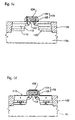
- FIGS. 1 a through 1 f are cross-sectional views illustrating semiconductor devices at various stages of fabrication according to the processes disclosed herein.
- device isolation layers 102 are formed in field regions of a semiconductor substrate 101 to define an active region by performing an isolation process, for example, a shallow trench isolation (STI) process.
- the semiconductor substrate 101 may be a single crystal silicon substrate of a first conduction type, which may be an n-type or a p-type. In the illustrated example process, the first conduction type is defined as an n-type.
- an oxide layer for a gate insulating layer is grown on the surface of the semiconductor substrate 101 .
- impurities for example, BE 2 ions, may be implanted into the substrate around the surface of the semiconductor substrate 101 to adjust the threshold voltage of a channel region.
- a conductive layer for a gate electrode is deposited on the oxide layer. The conductive layer and the oxide layer are then etched by using a photolithography process to form a gate electrode 104 and a gate insulating layer 103 on the active region of the semiconductor substrate 101 .
- a buffer oxide layer 105 to minimize the damage of the semiconductor substrate 101 due to later ion implantations is deposited on the semiconductor substrate including the gate electrode 104 .
- the buffer oxide layer 105 has a thickness between about 50 ⁇ and about 100 ⁇ .
- a first halo implant process is then performed.
- halo ions, first conductive type (n-type) impurities such as arsenic ions are implanted into the semiconductor substrate 101 with a dose that ranges from about 1.0 ⁇ 10 13 ions/cm 2 to about 5.0 ⁇ 10 14 ions/cm 2 at an implant energy ranging from about 10 kilo electron-Volts (keV) to about 50 keV.
- first halo implant regions (H 1 ) 106 are formed under the gate electrode 104 in the semiconductor substrate 101 .
- the impurity ions are implanted at an angle between about 20° and about 40° with respect to the direction perpendicular to the surface of the semiconductor substrate 101 .
- a low concentration ion implantation process is performed to form low concentration impurity regions 107 for LDD regions under sides of the gate electrode 104 in the semiconductor substrate 101 .
- second conduction type impurity ions for example, p-type boron ions, are implanted into the active region of the semiconductor substrate 101 with a dose that ranges from about 1.0 ⁇ 10 14 ions/cm 2 to about 1.0 ⁇ 10 15 ions/cm 2 at an implant energy ranging from about 10 keV to about 50 keV.
- the thermal treatment may be a rapid thermal treatment which is performed at a temperature between about 800° C. and about 1000° C. for about 10 seconds to about 30 seconds under an inert gas atmosphere.
- the inert gas may be nitrogen gas.
- a nitride layer 108 is deposited on the buffer oxide layer 105 .
- the nitride layer 108 has a thickness between about 500 ⁇ and about 1500 ⁇ .
- An etch-back process is then performed to dry-etch the nitride layer 108 until the buffer oxide layer 105 on the semiconductor substrate 101 is exposed.
- the etch-back process may be a reactive ion etching (RIE) with anisotropic etching characteristics.
- RIE reactive ion etching
- the buffer oxide layer 105 is dry-etched until the surface of the semiconductor substrate 101 is exposed.
- spacers 109 formed from the nitride layer 108 and the buffer oxide layer 105 are formed on the sidewalls of the gate electrode 104 .
- first conduction type (n-type) impurities for example, arsenic ions are implanted into the semiconductor substrate 101 with a dose that ranges from about 5.0 ⁇ 10 13 ions/cm 2 to about 5.0 ⁇ 10 14 ions/cm 2 at an implant energy ranging from about 5 keV to about 50 keV.
- second halo implant regions (H 2 ) 110 are formed under sides of the gate electrode 104 in the semiconductor substrate 101 .
- the impurity ions are implanted at right angle to the semiconductor substrate 101 .
- a high concentration ion implantation process is performed to form source/drain regions in the semiconductor substrate.
- second conduction type (p-type) impurity ions for example, B+ or BF 2+ ions, are implanted into the semiconductor substrate 101 to form high concentration impurity regions 111 .
- the impurity ions are implanted with a dose that ranges from about 1.0 ⁇ 10 15 ions/cm 2 to about 5.0 ⁇ 10 15 ions/cm 2 at an implant energy ranging from about 3 keV and about 50 keV.
- junction compensation ion regions (Jcomp) 112 are formed in the semiconductor substrate 101 between the high concentration impurity regions 111 and the second halo implant regions (H 2 ) 110 .
- the junction compensation ion regions 112 are formed additionally to the second halo implant regions (H 2 ) 110 to prevent the punch-through between the source region and the drain region.
- first conduction type (n-type) impurities for example, phosphorus ions are implanted into the semiconductor substrate 101 with a dose that ranges from about 1.0 ⁇ 10 14 ions/cm 2 to about 1.0 ⁇ 10 15 ions/cm 2 at an implant energy ranging from about 10 keV to about 60 keV.
- the second halo ion implantation has to be performed by controlling the implant energy so that the junction compensation ion regions formed are not overlapped with the second halo implant regions (H 2 ) 110 and/or the high concentration impurity regions 111 .
- a thermal treatment process is performed for the semiconductor substrate 101 to activate the impurities in the second halo implant regions (H 2 ) 110 , the high concentration impurity regions 111 , and the junction compensation ion regions 112 .
- the thermal treatment process may be a rapid thermal treatment which is performed at a temperature between about 900 ° C. and about 1050 ° C. for about 10 seconds to about 30 seconds under an inert gas atmosphere.
- the inert gas may be nitrogen gas.
- a self-aligned suicide (salicide) process is performed to form a salicide layer 113 on the top surface of the gate electrode 104 and on the source/drain regions.
- the salicide layer 113 may be formed of MoSi 2 , PdSi 2 , PtSI 2 , TaSi 2 , or WSi 2 , based on the high fusion point metal deposited.
- first halo implant regions under a gate electrode in a semiconductor substrate and forming source and drain regions, junction compensation ion regions, and second halo implant regions under sides of the gate electrode in the semiconductor substrate, the processes disclosed herein minimize punch-through between the source region and the drain region and improve the electric characteristics of a semiconductor device.
Landscapes
- Engineering & Computer Science (AREA)
- Physics & Mathematics (AREA)
- Microelectronics & Electronic Packaging (AREA)
- Power Engineering (AREA)
- Computer Hardware Design (AREA)
- General Physics & Mathematics (AREA)
- Condensed Matter Physics & Semiconductors (AREA)
- High Energy & Nuclear Physics (AREA)
- Manufacturing & Machinery (AREA)
- Ceramic Engineering (AREA)
- Health & Medical Sciences (AREA)
- Toxicology (AREA)
- Chemical & Material Sciences (AREA)
- Crystallography & Structural Chemistry (AREA)
- Spectroscopy & Molecular Physics (AREA)
- Insulated Gate Type Field-Effect Transistor (AREA)
Applications Claiming Priority (2)
| Application Number | Priority Date | Filing Date | Title |
|---|---|---|---|
| KR1020030095279A KR100574172B1 (ko) | 2003-12-23 | 2003-12-23 | 반도체 소자의 제조방법 |
| KR10-2003-0095279 | 2003-12-23 |
Publications (2)
| Publication Number | Publication Date |
|---|---|
| US20050136607A1 US20050136607A1 (en) | 2005-06-23 |
| US7151032B2 true US7151032B2 (en) | 2006-12-19 |
Family
ID=34675949
Family Applications (1)
| Application Number | Title | Priority Date | Filing Date |
|---|---|---|---|
| US11/021,731 Expired - Fee Related US7151032B2 (en) | 2003-12-23 | 2004-12-23 | Methods of fabricating semiconductor devices |
Country Status (2)
| Country | Link |
|---|---|
| US (1) | US7151032B2 (ko) |
| KR (1) | KR100574172B1 (ko) |
Cited By (5)
| Publication number | Priority date | Publication date | Assignee | Title |
|---|---|---|---|---|
| US20050151174A1 (en) * | 2003-12-31 | 2005-07-14 | Kim Tae W. | Semiconductor device and fabricating method thereof |
| US20070029608A1 (en) * | 2005-08-08 | 2007-02-08 | Taiwan Semiconductor Manufacturing Company, Ltd. | Offset spacers for CMOS transistors |
| US20090152646A1 (en) * | 2007-12-13 | 2009-06-18 | International Business Machines Corporation | Structure and method for manufacturing device with planar halo profile |
| US20130244388A1 (en) * | 2012-03-15 | 2013-09-19 | Globalfoundries Inc. | Methods for fabricating integrated circuits with reduced electrical parameter variation |
| US20220209012A1 (en) * | 2020-12-28 | 2022-06-30 | Texas Instruments Incorporated | Two-rotation gate-edge diode leakage reduction for mos transistors |
Families Citing this family (6)
| Publication number | Priority date | Publication date | Assignee | Title |
|---|---|---|---|---|
| KR100762876B1 (ko) * | 2005-12-28 | 2007-10-08 | 주식회사 하이닉스반도체 | 모스펫 소자의 제조방법 |
| US7449386B2 (en) * | 2006-11-16 | 2008-11-11 | Taiwan Semiconductor Manufacturing Company, Ltd. | Manufacturing method for semiconductor device to mitigate short channel effects |
| ITMI20070353A1 (it) * | 2007-02-23 | 2008-08-24 | Univ Padova | Transistore ad effetto di campo con giunzione metallo-semiconduttore. |
| US8299545B2 (en) * | 2010-01-28 | 2012-10-30 | International Business Machines Corporation | Method and structure to improve body effect and junction capacitance |
| CN107706097B (zh) * | 2017-09-14 | 2019-03-22 | 长鑫存储技术有限公司 | 半导体器件结构及其制备方法 |
| CN110634949B (zh) * | 2018-06-22 | 2023-03-28 | 立锜科技股份有限公司 | 高压元件及其制造方法 |
Citations (7)
| Publication number | Priority date | Publication date | Assignee | Title |
|---|---|---|---|---|
| US6017798A (en) * | 1995-07-07 | 2000-01-25 | Motorola, Inc. | FET with stable threshold voltage and method of manufacturing the same |
| US6194278B1 (en) | 1999-06-21 | 2001-02-27 | Infineon Technologies North America Corp. | Device performance by employing an improved method for forming halo implants |
| US6362054B1 (en) | 2000-03-13 | 2002-03-26 | Agere Systems Guardian Corp. | Method for fabricating MOS device with halo implanted region |
| US6518136B2 (en) | 2000-12-14 | 2003-02-11 | International Business Machines Corporation | Sacrificial polysilicon sidewall process and rapid thermal spike annealing for advance CMOS fabrication |
| US6555437B1 (en) * | 2001-04-27 | 2003-04-29 | Advanced Micro Devices, Inc. | Multiple halo implant in a MOSFET with raised source/drain structure |
| US6579751B2 (en) | 1999-09-01 | 2003-06-17 | Micron Technology, Inc. | Semiconductor processing methods of forming integrated circuitry |
| US6589847B1 (en) | 2000-08-03 | 2003-07-08 | Advanced Micro Devices, Inc. | Tilted counter-doped implant to sharpen halo profile |
-
2003
- 2003-12-23 KR KR1020030095279A patent/KR100574172B1/ko not_active IP Right Cessation
-
2004
- 2004-12-23 US US11/021,731 patent/US7151032B2/en not_active Expired - Fee Related
Patent Citations (7)
| Publication number | Priority date | Publication date | Assignee | Title |
|---|---|---|---|---|
| US6017798A (en) * | 1995-07-07 | 2000-01-25 | Motorola, Inc. | FET with stable threshold voltage and method of manufacturing the same |
| US6194278B1 (en) | 1999-06-21 | 2001-02-27 | Infineon Technologies North America Corp. | Device performance by employing an improved method for forming halo implants |
| US6579751B2 (en) | 1999-09-01 | 2003-06-17 | Micron Technology, Inc. | Semiconductor processing methods of forming integrated circuitry |
| US6362054B1 (en) | 2000-03-13 | 2002-03-26 | Agere Systems Guardian Corp. | Method for fabricating MOS device with halo implanted region |
| US6589847B1 (en) | 2000-08-03 | 2003-07-08 | Advanced Micro Devices, Inc. | Tilted counter-doped implant to sharpen halo profile |
| US6518136B2 (en) | 2000-12-14 | 2003-02-11 | International Business Machines Corporation | Sacrificial polysilicon sidewall process and rapid thermal spike annealing for advance CMOS fabrication |
| US6555437B1 (en) * | 2001-04-27 | 2003-04-29 | Advanced Micro Devices, Inc. | Multiple halo implant in a MOSFET with raised source/drain structure |
Cited By (8)
| Publication number | Priority date | Publication date | Assignee | Title |
|---|---|---|---|---|
| US20050151174A1 (en) * | 2003-12-31 | 2005-07-14 | Kim Tae W. | Semiconductor device and fabricating method thereof |
| US7767536B2 (en) * | 2003-12-31 | 2010-08-03 | Dongbu Electronics Co., Ltd. | Semiconductor device and fabricating method thereof |
| US20070029608A1 (en) * | 2005-08-08 | 2007-02-08 | Taiwan Semiconductor Manufacturing Company, Ltd. | Offset spacers for CMOS transistors |
| US20090152646A1 (en) * | 2007-12-13 | 2009-06-18 | International Business Machines Corporation | Structure and method for manufacturing device with planar halo profile |
| US7883976B2 (en) | 2007-12-13 | 2011-02-08 | International Business Machines Corporation | Structure and method for manufacturing device with planar halo profile |
| US20130244388A1 (en) * | 2012-03-15 | 2013-09-19 | Globalfoundries Inc. | Methods for fabricating integrated circuits with reduced electrical parameter variation |
| US20220209012A1 (en) * | 2020-12-28 | 2022-06-30 | Texas Instruments Incorporated | Two-rotation gate-edge diode leakage reduction for mos transistors |
| US12009423B2 (en) * | 2020-12-28 | 2024-06-11 | Texas Instruments Incorporated | Two-rotation gate-edge diode leakage reduction for MOS transistors |
Also Published As
| Publication number | Publication date |
|---|---|
| KR20050064011A (ko) | 2005-06-29 |
| US20050136607A1 (en) | 2005-06-23 |
| KR100574172B1 (ko) | 2006-04-27 |
Similar Documents
| Publication | Publication Date | Title |
|---|---|---|
| KR100588786B1 (ko) | 반도체 소자 제조방법 | |
| US6184112B1 (en) | Method of forming a MOSFET transistor with a shallow abrupt retrograde dopant profile | |
| US6500720B2 (en) | Method of manufacturing semiconductor device | |
| EP0789400A2 (en) | Semiconductor device and method for fabricating the same | |
| KR20010050044A (ko) | 소스/드레인 접합부에서 측방 도핑 분포를 급경사지게형성하는 방법 및 소자 | |
| US6838329B2 (en) | High concentration indium fluorine retrograde wells | |
| US5869378A (en) | Method of reducing overlap between gate electrode and LDD region | |
| US7071069B2 (en) | Shallow amorphizing implant for gettering of deep secondary end of range defects | |
| US7151032B2 (en) | Methods of fabricating semiconductor devices | |
| US6083798A (en) | Method of producing a metal oxide semiconductor device with raised source/drain | |
| US7303967B2 (en) | Method for fabricating transistor of semiconductor device | |
| US6380021B1 (en) | Ultra-shallow junction formation by novel process sequence for PMOSFET | |
| US7235450B2 (en) | Methods for fabricating semiconductor devices | |
| JP4186247B2 (ja) | 半導体装置の製造方法および導電性シリコン膜の形成方法 | |
| KR100475538B1 (ko) | 반도체 소자의 제조방법 | |
| KR100588787B1 (ko) | 반도체 소자 제조방법 | |
| US7160783B2 (en) | MOS transistor and method of manufacturing the same | |
| KR100940438B1 (ko) | 반도체 소자의 제조 방법 | |
| KR100588784B1 (ko) | 반도체 소자 제조방법 | |
| KR100531120B1 (ko) | 반도체 소자 제조방법 | |
| KR100598284B1 (ko) | 반도체 소자 제조방법 | |
| US20080003788A1 (en) | Method of manufacturing semiconductor device | |
| KR101016337B1 (ko) | 반도체 소자의 제조 방법 | |
| KR100778862B1 (ko) | 반도체 소자 및 그 제조방법 | |
| KR100550381B1 (ko) | 반도체 소자 및 그 제조 방법 |
Legal Events
| Date | Code | Title | Description |
|---|---|---|---|
| AS | Assignment |
Owner name: DONGBUANAM SEMICONDUCTOR, INC., KOREA, REPUBLIC OF Free format text: ASSIGNMENT OF ASSIGNORS INTEREST;ASSIGNOR:KIM, HAG DONG;REEL/FRAME:016517/0250 Effective date: 20041222 Owner name: DONGBUANAM SEMICONDUCTOR, INC., KOREA, REPUBLIC OF Free format text: ASSIGNMENT OF ASSIGNORS INTEREST;ASSIGNOR:KIM, HAG DONG;REEL/FRAME:016517/0175 Effective date: 20041222 |
|
| AS | Assignment |
Owner name: DONGBU ELECTRONICS CO., LTD., KOREA, REPUBLIC OF Free format text: CHANGE OF NAME;ASSIGNOR:DONGBU ANAM SEMICONDUCTORS, INC;REEL/FRAME:017718/0964 Effective date: 20060410 |
|
| FEPP | Fee payment procedure |
Free format text: PAYOR NUMBER ASSIGNED (ORIGINAL EVENT CODE: ASPN); ENTITY STATUS OF PATENT OWNER: LARGE ENTITY |
|
| CC | Certificate of correction | ||
| FEPP | Fee payment procedure |
Free format text: PAYER NUMBER DE-ASSIGNED (ORIGINAL EVENT CODE: RMPN); ENTITY STATUS OF PATENT OWNER: LARGE ENTITY Free format text: PAYOR NUMBER ASSIGNED (ORIGINAL EVENT CODE: ASPN); ENTITY STATUS OF PATENT OWNER: LARGE ENTITY |
|
| FPAY | Fee payment |
Year of fee payment: 4 |
|
| REMI | Maintenance fee reminder mailed | ||
| LAPS | Lapse for failure to pay maintenance fees | ||
| STCH | Information on status: patent discontinuation |
Free format text: PATENT EXPIRED DUE TO NONPAYMENT OF MAINTENANCE FEES UNDER 37 CFR 1.362 |
|
| FP | Lapsed due to failure to pay maintenance fee |
Effective date: 20141219 |