US7138993B2 - LCD with integrated switches for DC restore - Google Patents
LCD with integrated switches for DC restore Download PDFInfo
- Publication number
- US7138993B2 US7138993B2 US10/370,038 US37003803A US7138993B2 US 7138993 B2 US7138993 B2 US 7138993B2 US 37003803 A US37003803 A US 37003803A US 7138993 B2 US7138993 B2 US 7138993B2
- Authority
- US
- United States
- Prior art keywords
- video signal
- coupled
- display
- input video
- coupling capacitor
- Prior art date
- Legal status (The legal status is an assumption and is not a legal conclusion. Google has not performed a legal analysis and makes no representation as to the accuracy of the status listed.)
- Expired - Lifetime, expires
Links
- 239000003990 capacitor Substances 0.000 claims abstract description 59
- 238000010168 coupling process Methods 0.000 claims abstract description 59
- 238000005859 coupling reaction Methods 0.000 claims abstract description 59
- 230000008878 coupling Effects 0.000 claims abstract description 50
- 239000004973 liquid crystal related substance Substances 0.000 claims abstract description 26
- 238000000034 method Methods 0.000 claims description 13
- 230000000295 complement effect Effects 0.000 claims description 4
- 238000010586 diagram Methods 0.000 description 53
- 230000005540 biological transmission Effects 0.000 description 8
- 238000013459 approach Methods 0.000 description 7
- 108010020053 Staphylococcus warneri lipase 2 Proteins 0.000 description 6
- 230000008901 benefit Effects 0.000 description 6
- 101100242307 Saccharomyces cerevisiae (strain ATCC 204508 / S288c) SWH1 gene Proteins 0.000 description 5
- 239000011159 matrix material Substances 0.000 description 5
- 230000000694 effects Effects 0.000 description 4
- 239000000243 solution Substances 0.000 description 3
- 101100509370 Saccharomyces cerevisiae (strain ATCC 204508 / S288c) ISW1 gene Proteins 0.000 description 2
- 230000000740 bleeding effect Effects 0.000 description 2
- 238000002347 injection Methods 0.000 description 2
- 239000007924 injection Substances 0.000 description 2
- 101150045244 ISW2 gene Proteins 0.000 description 1
- 102000044753 ISWI Human genes 0.000 description 1
- 108700007305 ISWI Proteins 0.000 description 1
- 239000008186 active pharmaceutical agent Substances 0.000 description 1
- 230000015556 catabolic process Effects 0.000 description 1
- 239000000356 contaminant Substances 0.000 description 1
- 210000002858 crystal cell Anatomy 0.000 description 1
- 230000009977 dual effect Effects 0.000 description 1
- 238000005516 engineering process Methods 0.000 description 1
- 230000010354 integration Effects 0.000 description 1
Images


Classifications
-
- G—PHYSICS
- G09—EDUCATION; CRYPTOGRAPHY; DISPLAY; ADVERTISING; SEALS
- G09G—ARRANGEMENTS OR CIRCUITS FOR CONTROL OF INDICATING DEVICES USING STATIC MEANS TO PRESENT VARIABLE INFORMATION
- G09G3/00—Control arrangements or circuits, of interest only in connection with visual indicators other than cathode-ray tubes
- G09G3/20—Control arrangements or circuits, of interest only in connection with visual indicators other than cathode-ray tubes for presentation of an assembly of a number of characters, e.g. a page, by composing the assembly by combination of individual elements arranged in a matrix no fixed position being assigned to or needed to be assigned to the individual characters or partial characters
- G09G3/34—Control arrangements or circuits, of interest only in connection with visual indicators other than cathode-ray tubes for presentation of an assembly of a number of characters, e.g. a page, by composing the assembly by combination of individual elements arranged in a matrix no fixed position being assigned to or needed to be assigned to the individual characters or partial characters by control of light from an independent source
- G09G3/36—Control arrangements or circuits, of interest only in connection with visual indicators other than cathode-ray tubes for presentation of an assembly of a number of characters, e.g. a page, by composing the assembly by combination of individual elements arranged in a matrix no fixed position being assigned to or needed to be assigned to the individual characters or partial characters by control of light from an independent source using liquid crystals
- G09G3/3611—Control of matrices with row and column drivers
- G09G3/3614—Control of polarity reversal in general
-
- G—PHYSICS
- G09—EDUCATION; CRYPTOGRAPHY; DISPLAY; ADVERTISING; SEALS
- G09G—ARRANGEMENTS OR CIRCUITS FOR CONTROL OF INDICATING DEVICES USING STATIC MEANS TO PRESENT VARIABLE INFORMATION
- G09G3/00—Control arrangements or circuits, of interest only in connection with visual indicators other than cathode-ray tubes
- G09G3/20—Control arrangements or circuits, of interest only in connection with visual indicators other than cathode-ray tubes for presentation of an assembly of a number of characters, e.g. a page, by composing the assembly by combination of individual elements arranged in a matrix no fixed position being assigned to or needed to be assigned to the individual characters or partial characters
-
- G—PHYSICS
- G09—EDUCATION; CRYPTOGRAPHY; DISPLAY; ADVERTISING; SEALS
- G09G—ARRANGEMENTS OR CIRCUITS FOR CONTROL OF INDICATING DEVICES USING STATIC MEANS TO PRESENT VARIABLE INFORMATION
- G09G2320/00—Control of display operating conditions
- G09G2320/02—Improving the quality of display appearance
- G09G2320/0204—Compensation of DC component across the pixels in flat panels
-
- G—PHYSICS
- G09—EDUCATION; CRYPTOGRAPHY; DISPLAY; ADVERTISING; SEALS
- G09G—ARRANGEMENTS OR CIRCUITS FOR CONTROL OF INDICATING DEVICES USING STATIC MEANS TO PRESENT VARIABLE INFORMATION
- G09G2330/00—Aspects of power supply; Aspects of display protection and defect management
- G09G2330/02—Details of power systems and of start or stop of display operation
- G09G2330/026—Arrangements or methods related to booting a display
-
- G—PHYSICS
- G09—EDUCATION; CRYPTOGRAPHY; DISPLAY; ADVERTISING; SEALS
- G09G—ARRANGEMENTS OR CIRCUITS FOR CONTROL OF INDICATING DEVICES USING STATIC MEANS TO PRESENT VARIABLE INFORMATION
- G09G3/00—Control arrangements or circuits, of interest only in connection with visual indicators other than cathode-ray tubes
- G09G3/20—Control arrangements or circuits, of interest only in connection with visual indicators other than cathode-ray tubes for presentation of an assembly of a number of characters, e.g. a page, by composing the assembly by combination of individual elements arranged in a matrix no fixed position being assigned to or needed to be assigned to the individual characters or partial characters
- G09G3/34—Control arrangements or circuits, of interest only in connection with visual indicators other than cathode-ray tubes for presentation of an assembly of a number of characters, e.g. a page, by composing the assembly by combination of individual elements arranged in a matrix no fixed position being assigned to or needed to be assigned to the individual characters or partial characters by control of light from an independent source
- G09G3/36—Control arrangements or circuits, of interest only in connection with visual indicators other than cathode-ray tubes for presentation of an assembly of a number of characters, e.g. a page, by composing the assembly by combination of individual elements arranged in a matrix no fixed position being assigned to or needed to be assigned to the individual characters or partial characters by control of light from an independent source using liquid crystals
- G09G3/3611—Control of matrices with row and column drivers
- G09G3/3685—Details of drivers for data electrodes
- G09G3/3688—Details of drivers for data electrodes suitable for active matrices only
Definitions
- LCDs liquid crystal displays
- DC direct current
- FIG. 1 A graph of transmission versus voltage of an LCD is shown in FIG. 1 , showing high transmission with zero voltage and low transmission with either positive or negative voltage.
- a positive voltage cannot be placed on the LCD.
- a steady state DC voltage may damage the display by, for example, causing contaminants to plate one side or the other of the liquid crystal cell.
- DC restore DC restore
- the voltage applied to the LCD is flipped back and forth (alternated) between high-black, low-black, high-black, low-black.
- FIGS. 2A–2D There are different scenarios for preserving zero (0) DC, as shown in the series of succeeding frames of FIGS. 2A–2D .
- One scenario uses column inversion as shown in FIG. 2A , where one frame is written with all the columns having alternating polarity, positive-negative, positive-negative. In the next frame all the columns are written negative-positive, negative-positive. In the succeeding frame, all the columns are again written positive-negative, positive-negative.
- FIG. 2B frame inversion can be used where the first frame is written with all positives and the next frame is written with all negatives. The succeeding frame is again written with all positives.
- FIG. 2A shows column inversion as shown in FIG. 2A , where one frame is written with all the columns having alternating polarity, positive-negative, positive-negative. In the next frame all the columns are written negative-positive, negative-positive. In the succeeding frame, all the columns are again written positive-negative, positive-negative.
- FIG. 2B frame inversion can be
- pixel inversion can be used which produces a checkerboard like effect in the first frame and an inverted effect in the second frame.
- the checkerboard like effect matches that of the first frame.
- row inversion can be used where all the rows are alternating polarity, positive-negative, positive-negative. In the next frame all the rows are written negative-positive, negative-positive. In the third frame, the rows are again written positive-negative, negative-negative.
- Suitable DC-coupled display driver circuits require high supply voltages.
- Some AC-coupled display driver approaches have an advantage of being able to use lower voltage amplifiers.
- external switches required for DC restore in such systems still must handle higher voltages.
- the present invention provides a more desirable approach for AC-coupled display driver circuitry.
- one or more DC-restore switches are integrated within a liquid crystal display.
- the integrated switches can be implemented in the same high-voltage process used for the display's internal circuits.
- An advantage is that no external integrated circuit is needed for the DC-restore switches, and system input amplifiers can be integrated with other components on a low-voltage integrated circuit.
- a liquid crystal display system includes a coupling capacitor coupled at one end to a system input video signal, the coupling capacitor providing a display input video signal having a DC level offset.
- a liquid crystal display device coupled to another end of the coupling capacitor receives the first display input video signal at a video input for driving the display device.
- a switch integrated within the display device provides DC restore to the coupling capacitor.
- a second coupling capacitor coupled at one end to the system input video signal provides a second display input video signal having a second DC level offset.
- the liquid crystal display device includes a second video input coupled to another end of the second coupling capacitor to receive the second display input video signal for driving the display device.
- a second switch integrated within the display device provides DC restore to the second coupling capacitor.
- the integrated switches are operable to provide DC restore to the coupling capacitors when operated during a retrace interval of the system input video signal.
- a liquid crystal display system features a single system input video signal.
- An amplifier having switchable gain polarity coupled to the system input video signal provides an amplified system input video signal.
- a first coupling capacitor coupled at one end to the amplifier provides a first display input video signal having a first DC level offset.
- a second coupling capacitor coupled at one end to the amplifier provides a second display input video signal having a second DC level offset.
- a liquid crystal display device receives the first and second display input video signals for driving the display device.
- First and second switches provide DC restore to the first and second coupling capacitors, respectively. The first and second switches may be external to the display device or integrated into the display device.
- FIG. 1 is a transmission versus voltage diagram.
- FIGS. 2A–2D are diagrams showing successive frames using column inversion, frame inversion, pixel inversion and row inversion, respectively.
- FIG. 3A is a schematic circuit diagram of a DC-coupled driver circuit with two amplifiers.
- FIG. 3B is a waveform diagram for signals applied in the circuit of FIG. 3A .
- FIG. 4A is a schematic circuit diagram of a DC-coupled driver circuit with a single amplifier having switchable gain polarity.
- FIG. 4B is a waveform diagram for signals applied in the circuit of FIG. 4A .
- FIG. 5 is a waveform diagram related to driving a common electrode with an AC signal.
- FIG. 6A is a schematic circuit diagram of an AC-coupled driver circuit with two amplifiers, configured for resetting the display to black.
- FIG. 6B is a schematic circuit diagram of an AC-coupled driver circuit with two amplifiers, configured for resetting the display to white.
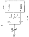
- FIG. 7A is a schematic circuit diagram of an AC-coupled driver circuit configured with a single amplifier having switchable gain polarity and with switches restoring DC by resetting to the white level, in accordance with the principles of the present invention.
- FIG. 7B is a waveform diagram for signals applied in the circuit of FIG. 7A .
- FIG. 7C is a schematic circuit diagram of an AC-coupled driver circuit configured with a single amplifier having switchable gain polarity and with switches restoring DC by resetting to the black levels, in accordance with the principles of the present invention.
- FIG. 7D is a waveform diagram for signals applied in the circuit of FIG. 7C .
- FIG. 8 is a schematic circuit diagram of a display highlighting one row of pixels.
- FIG. 9 is a diagram of a display highlighting a bleed through effect.
- FIG. 10A is a schematic circuit diagram of an AC-coupled display with two integrated switches configured for DC restore while resetting the display to white in accordance with the principles of the present invention.
- FIG. 10B is a schematic circuit diagram similar to the diagram of FIG. 10A with a 5 volt voltage shift in accordance with the principles of the present invention.
- FIG. 10C is a schematic circuit diagram of an AC-coupled display with two integrated switches configured for DC restore while resetting the display to black in accordance with the principles of the present invention.
- FIG. 10D is a schematic circuit diagram of an AC-coupled display with a single system input, a single display input, and an integrated switch configured for DC restore with display reset to white in accordance with the principles of the present invention.
- FIG. 10E is a schematic circuit diagram of an AC-coupled display with a single system input, a single display input, and two integrated switches configured for DC restore with display reset to black according to the principles of the present invention.
- FIG. 10F is a schematic circuit diagram of an AC-coupled display with a single system input, a single display input, and an integrated switch configured for DC restore with display reset to white and AC common in accordance with the principles of the present invention.
- FIG. 10G is a schematic circuit diagram similar to FIG. 10F , using an AC-coupled common signal and integrated common switch, in accordance with the principles of the present invention.
- FIG. 10H is a schematic circuit diagram of an AC-coupled driver circuit configured with a single amplifier having switchable gain polarity and with integrated switches restoring DC by resetting to the white level, in accordance with the principles of the present invention.
- FIG. 10I is a schematic circuit diagram of an AC-coupled driver circuit configured with a single amplifier having switchable gain polarity and with integrated switches restoring DC by resetting to the black levels, in accordance with the principles of the present invention.
- FIG. 11A is a diagram of an NMOS switch for use with a video high display input signal in any of the embodiments of FIGS. 10A–10B .
- FIG. 11B is a diagram of a PMOS switch for use with a video low display input signal in the embodiments of FIGS. 10A–10B .
- FIG. 11C is a diagram of an NMOS switch for use with a single video display input signal in the embodiments of FIG. 10D or FIG. 10F , in which the video input may is swing above or below VCOM.
- FIG. 11D is a diagram of a pair of NMOS and PMOS switches for use with video high and video low input signals in the embodiment of FIG. 10C .
- FIG. 11E is a diagram of a pair of NMOS and PMOS switches for use with a video input signals in the embodiment of FIG. 10E .
- FIG. 12A is a schematic circuit diagram of a bootstrapping circuit for use with the embodiments of FIGS. 10A–10B .
- FIG. 12B is a waveform diagram of control signals for the bootstrapping circuit of FIG. 12A .
- FIG. 13A is a schematic circuit diagram of a bootstrapping circuit for use with the embodiments of FIG. 10D or FIG. 10F .
- FIG. 13B is a waveform diagram of control signals for the bootstrapping circuit of FIG. 13A .
- FIG. 14 is a schematic diagram of a charge injection cancellation circuit for use with the integrated switches of the embodiments of FIGS. 10A–10F .
- FIG. 15 is a schematic circuit diagram of an integrated circuit active matrix display for use in embodiments according to the present invention.
- FIG. 3A shows a DC-coupled driver circuit 10 with two video signals, video high (VIDH) and video low (VIDL), coupled to a liquid crystal display device 30 .
- the signals VIDH and VIDL are complementary signals that drive an active matrix of pixel elements not shown for clarity.
- VCOM common electrode
- VIDH the signals are centered around 5 volts, which is the voltage applied to the common electrode (VCOM) of all pixels.
- VCOM common electrode
- VIDH is 8 volts
- the pixel voltage is +3 volts (black).
- VIDL ranges from 5 volts white to 2 volts black.
- the input video signal swing is typically 1 volt, therefore positive and negative amplifiers 20 are needed with matching gains of +3 and ⁇ 3 volts.
- FIG. 3B is a waveform diagram of video signals applied in the circuit 10 of FIG. 3A using row inversion.
- FIG. 4A To avoid underutilized amplifiers in the situation just described, row inversion displays typically use a driver circuit such as that shown in FIG. 4A .
- a single video signal (VID) is driven by a single amplifier 22 coupled to display 32 .
- the amplifier polarity is switched for positive or negative gain.
- VID swings from white to high black (as does VIDH in FIG. 3A ).
- VIDH VIDL
- FIG. 4B is a waveform diagram of video signals applied in the circuit of FIG. 4A using row inversion.
- VID signal swing One widely-used technique for reducing the VID signal swing is to drive the common electrode VCOM with an AC signal.
- This AC-common drive scheme is shown in the waveform diagram of FIG. 5 .
- the VCOM level is reduced to 2 volts when writing positive rows, so that the +3V black level is written with VID at 5 volts.
- Negative rows drive VCOM to 5 volts, so that 3V black is written with VID at 2 volts.
- One disadvantage of AC-common drive is that it requires additional circuitry to switch the VCOM level. Another disadvantage is incompatibility with some pixel designs and scanner circuits.
- the required video bandwidth may be greater than can be practically supplied on a single VID signal or pair of VIDH and VIDL signals.
- Examples include higher resolution displays with a large number (> ⁇ 300 k) pixels, and displays intended to operate at unusually high frame rates (> ⁇ 60 Hz). These displays may use multiple VID inputs or pairs of VIDH and VIDL inputs to achieve the necessary bandwidth. Color displays may also use multiple video inputs for separate red, green, and blue component signals. For clarity, the following discussion continues to refer to single inputs or input pairs, but the ideas and techniques described may be readily scaled for displays with multiple inputs.
- a disadvantage of the DC-coupled systems is their high supply voltage. If VCOM is held at a DC level, then at least one amplifier will require a supply exceeding the high black level of 8 volts. Even with AC-common drive, the maximum video voltage level of 5 volts is significantly greater than the actual 3-volt swing, because of the 2-volt minimum level imposed by the display's circuits.
- the high supply voltages increase the system power dissipation, and also limit the technologies available for implementing the video amplifiers. For example, an 8-volt video amplifier may require a relatively expensive BiCMOS process.
- a 5-volt amplifier may be implemented in a specialized analog CMOS process.
- a more desirable solution would be a rail-to-rail amplifier driving 3-volt video with a 3.3-volt supply and implemented in a conventional CMOS logic process.
- CMOS processes are widely available and relatively inexpensive.
- the 3.3-volt CMOS solution may lead to higher integration, since the amplifier may be integrated on the same chip as other system components.
- FIG. 6A shows a circuit 14 with low-voltage amplifiers 20 and AC-coupled drive for column inversion.
- Capacitors C H and C L are used to shift the DC level. The outputs of both amplifier swing 0–3 volts on the left side of the capacitors, but on the right side of the capacitors the display 30 sees 5–8 volts on VIDH and 2–5 volts on VIDL. For proper operation, the voltage offsets across C H and C L must be maintained at +5 and +2 volts, respectively. These offsets are periodically refreshed by driving the input video to black and closing DC-restore switches SWH 2 , SWL 2 .
- FIG. 6B shows a similar AC-coupled circuit 16 , but with both DC restore switches SWH 1 , SWL 1 connected to the 5-volt common level.
- the offset voltages across C H and C L are the same as in FIG. 6A , but in this case, the input signal is driven to white to perform the refresh.
- any convenient level may be used for this DC-restore technique: black, white, gray, or perhaps the sync level.
- black, white, gray, or perhaps the sync level is any convenient level.
- One advantage of resetting to white is that a single +5V reference supply may be used for both switches.
- reset-to-black may be preferred when using standard video signals which already provide a black “blanking period” during horizontal retrace.
- FIGS. 7A and 7 C show AC-coupled circuits 18 and 40 , respectively, for use with row inversion in accordance with the principles of the present invention.
- the amplifier polarities in the circuits of FIGS. 7A and 7C are switchable.
- the minimum and maximum signal levels are the same for both polarities.
- the two switches (SWH 1 , SWL 1 in FIG. 7A ; SWH 2 , SWL 2 in FIG. 7C ) are operated independently, and the VIDH and VIDL signals are reset at different times.
- the circuit of FIG. 7A resets to the white level.
- capacitor C H is reset by closing SWH 1 to connect VIDH to +5V while the amplifier output is low (0V)
- C L is reset by closing SWL 1 to connect VIDL to +5V while the amplifier output is high (3V).
- the circuit of FIG. 7C resets to the black levels.
- capacitor C H is reset by closing SWH 2 to connect VIDH to +8V while the amplifier output is high (3V)
- C L is reset by closing SWL 2 to connect VIDL to +2V while the amplifier output is low (0V).
- FIG. 8 shows a video line VIDH/L switched through switches SW 1 –SW 5 to several capacitors C1–C5, representing the capacitive loads of all columns driven from that video line.
- the switches SW 1 –SW 5 represent transmission gates that switch video voltage onto column capacitance. As each transmission gate switch SW 1 –SW 5 is closed, a small charge is transferred from the column capacitance and an error signal accumulates on the external coupling capacitor. The error increases as the scan proceeds further across the display.
- FIG. 9 illustrates a display 30 A that includes an image area 32 having a gray image portion (B) and a black image portion (A). While scanning the black image portion (A), the area (AA) to the right is slightly a different shade of gray than the gray image above it. This is likely because a different charge was transferred onto the capacitors in that area. A solution is to make the capacitors larger so that they can absorb whatever charge is transferred. The same amount of charge on a larger capacitor results in a smaller error signal voltage, thereby preventing this bleeding effect.
- the AC-coupled drive approaches ( FIGS. 6A , 6 B, 7 A and 7 C) permit the use of lower voltage amplifiers, because no signals on the left side of the capacitors exceed 3.3V.
- the DC-restore switches (SWH 1 , SWL 1 , SWH 2 , SWL 2 ) are on the right side of the capacitors, and hence must handle higher voltages.
- FIGS. 10A–10F show several embodiments of a more desirable approach for AC-coupled drive circuitry in accordance with the present invention.
- one or more DC-restore switches are integrated inside the LCD.
- the switches can be implemented in the same high-voltage process used for the display's internal circuits.
- FIGS. 10A–10C illustrate embodiments of AC-coupled drive circuits that feature two display inputs and have two integrated switches that are independently operated.
- FIG. 10A illustrates a circuit 42 that includes a display 50 with integrated switches ISWH 1 , ISWL 1 configured for DC restore while resetting the display to white.
- FIG. 10B shows a circuit 44 that is similar to the display diagram of FIG. 10A but with integrated switches ISWH 2 , ISWL 2 configured for a 5 volt voltage shift at display 52 .
- the circuit 46 of FIG. 10C includes integrated switches ISWH 3 , ISWL 3 that are configured for DC restore while resetting the display 54 to black.
- FIGS. 10D–10E illustrate AC-coupled drive circuits 48 , 70 that feature a single system input, a single display input, and integrated switching.
- the output voltage swing of amplifier 22 A is 6V, the same as in the DC-coupled case of FIG. 4A .
- the maximum amplifier output voltage is reduced from 8V in FIG. 4A to 6V in FIGS. 10D and 10E .
- the reduced output voltage may allow the amplifier 22 A to be operated at a lower supply voltage, thereby saving power.
- the circuit 48 of FIG. 10D has a single integrated switch ISW 1 configured for DC restore with display 56 reset to white. The switch ISW 1 is closed periodically with the input video at the white level.
- 10E includes two integrated switches ISWH 4 , ISWL 4 configured for DC restore with display 58 reset to black.
- One or both of the switches ISWH 4 and ISWL 4 may be used.
- the switches are operated independently, with ISWH 4 closed when the amplifier output is at the high black level (6V), and/or with ISWL 4 closed when the amplifier output is at the low black level (0V). If both switches are used, then the +8V and +2V references should be well matched to the limits of the amplifier output swing.
- FIG. 10F illustrates a display drive circuit 72 with AC-coupled video, an AC-common signal, and integrated switching.
- the VCOM signal levels are the same as in the DC-coupled case of FIG. 5 .
- the use of AC-coupled video reduces the maximum voltage level required at the amplifier output.
- DC restore is performed by closing switch ISW 2 integrated within display 60 while the input video signal is at the white level (1V).
- FIG. 10G illustrates a display drive circuit 74 with AC-coupled video, an AC-common signal, and integrated switching for both video and VCOM signals at display 62 .
- the video signal is reset to the white level by closing switch ISW 3 and connecting VID to VCOM.
- the VCOM level is restored by closing ISW 4 and connecting VCOM to a (+2V) reference level.
- FIGS. 10H and 10I illustrate the external switches (SWH 1 , SWL 1 , SWH 2 , SWL 2 ) in the AC-coupled drive circuits of FIGS. 7A and 7C , respectively.
- FIG. 10H illustrates display driver circuit 76 with integrated switches ISWH 5 , ISWL 5 at display 64 .
- FIG. 10I illustrates display driver circuit 78 with integrated switches ISWH 6 , ISWL 6 at display 66 .
- FIG. 11A is a diagram of an NMOS switch 80 for use with a video high display input signal in any of the embodiments of FIGS. 10A–10B .
- the switch is controlled by gate voltage VGH.
- FIG. 11B is a diagram of a PMOS switch 82 for use with a video low display input signal in the embodiments of FIGS. 10A–10B .
- the switch 82 is controlled by gate voltage VGL.
- FIG. 11C is a diagram of an NMOS switch 84 for use with a single video display input signal in the embodiments of FIG. 10D or FIG. 10F .
- the switch is shown coupled to display input VID and common voltage VCOM, with VMAX>VCOM and VMIN ⁇ VCOM.
- the switch 84 is controlled by gate voltage VG.
- the switch is gated off when VG ⁇ VMIN+VTN, which will be less than VCOM+VTN.
- the switch is gated on when VG>VMAX+VTN.
- FIG. 11D is a diagram of a pair of NMOS and PMOS switches 86 , 88 for use with video high and video low input signals in the embodiment of FIG. 10C .
- the NMOS switch 88 is shown coupled to display input VIDL and the low black reference level (+2V)
- the PMOS switch 86 is shown coupled to the display input VIDH and the high black reference level (+8V). In this case VIDH is less than the high black reference (+8V), and VIDL is greater than the low black reference level (+2V).
- the PMOS switch is controlled by gate voltage VGH
- the NMOS switch is controlled by gate voltage VGL.
- FIG. 11E is similar to FIG. 11D with switches 90 , 92 , but with a single video input as in the embodiment of FIG. 10E .
- FIG. 12A is a schematic circuit diagram of a bootstrapping circuit 102 for use with the embodiments of FIGS. 10A–10B .
- FIG. 12B is a waveform diagram of control signals for the bootstrapping circuit of FIG. 12A .
- FIG. 13A is a schematic circuit diagram of a bootstrapping circuit 110 for use with the embodiments of FIG. 10D or FIG. 10F .
- FIG. 13B is a waveform diagram of control signals for the bootstrapping circuit of FIG. 13A .
- the bootstrapping circuit 102 ( FIG. 12A ) includes switches 104 , 106 , 108 .
- the timing diagram of FIG. 12B begins with gate voltage g held at the VCOM level, and the NMOS switch therefore open. Signal s* is then driven low to disconnect g from VCOM. Signal u* is then pulsed low, pulling gate Voltage g up toward VDD through diode D 1 . When signal p is then pulsed high, gate voltage g is capacitively coupled to a voltage higher than VDD, thereby increasing the switch conductance.
- the dual of circuit FIG. 12A may be used to drive a PMOS switch.
- the circuit 110 of FIG. 13A performs a bootstrap function similar to that of FIG. 12A , while also allowing the gate voltage g to be driven below VCOM, as is required for the embodiments of FIG. 10D or FIG. 10F .
- Node g is driven by two inverters 109 , 111 which have their negative supplies connected to signal p.
- Signal y is an un-boosted input signal.
- the circuit configuration ensures that no transistor's drain-to-source voltage V DS exceeds (VDD ⁇ VSS), which may avoid transistor breakdown and improve circuit reliability.
- FIG. 14 is a schematic diagram of a charge injection cancellation circuit 120 for use with the integrated switches of the embodiments of FIGS. 10A–10G .
- switch transistor 122 of size (W/L) turns off, its channel charge is injected onto the source and drain nodes VCOM and VID. Assuming that each node receives half of the charge, the charge may be cancelled by a compensation transistor 124 of size ((W/2)/L).
- the gate of the cancellation circuit is driven by the inverse signal of the switch gate, so that the cancellation FET turns on soon after the switch transistor turns off.
- the circuit 200 includes data scanners 202 and 204 , select scanner 206 , active matrix pixel array 208 , a plurality of transmission gates 210 and 212 , control logic 216 , integrated switches 217 and 219 , level shift 218 , and power control 220 .
- the integrated scanners drive the active matrix pixel array 208 .
- the pixel array 208 has a plurality of pixel elements 214 .
- the RGT input selects one of the two data scanners for left-to-right ( 202 ) or right-to-left ( 204 ) horizontal scanning.
- the select scanner 206 scans vertically from top to bottom.
- the data scanners 202 , 204 accept logic-level clock inputs directly from the input pads, thereby reducing the power dissipation and skew otherwise associated with internal clock drivers.
- Complementary video signals are accepted on the AC-coupled VIDH and VIDL inputs, with internal switches 217 and 219 , respectively, restoring DC levels during the horizontal retrace interval.
- the VIDH and VIDL signals carry video signals to the transmission gates 210 and 212 .
Landscapes
- Engineering & Computer Science (AREA)
- Physics & Mathematics (AREA)
- Computer Hardware Design (AREA)
- General Physics & Mathematics (AREA)
- Theoretical Computer Science (AREA)
- Chemical & Material Sciences (AREA)
- Crystallography & Structural Chemistry (AREA)
- Liquid Crystal Display Device Control (AREA)
- Control Of Indicators Other Than Cathode Ray Tubes (AREA)
Priority Applications (1)
| Application Number | Priority Date | Filing Date | Title |
|---|---|---|---|
| US10/370,038 US7138993B2 (en) | 2002-02-19 | 2003-02-19 | LCD with integrated switches for DC restore |
Applications Claiming Priority (2)
| Application Number | Priority Date | Filing Date | Title |
|---|---|---|---|
| US35794402P | 2002-02-19 | 2002-02-19 | |
| US10/370,038 US7138993B2 (en) | 2002-02-19 | 2003-02-19 | LCD with integrated switches for DC restore |
Publications (2)
| Publication Number | Publication Date |
|---|---|
| US20030174113A1 US20030174113A1 (en) | 2003-09-18 |
| US7138993B2 true US7138993B2 (en) | 2006-11-21 |
Family
ID=27757682
Family Applications (1)
| Application Number | Title | Priority Date | Filing Date |
|---|---|---|---|
| US10/370,038 Expired - Lifetime US7138993B2 (en) | 2002-02-19 | 2003-02-19 | LCD with integrated switches for DC restore |
Country Status (5)
| Country | Link |
|---|---|
| US (1) | US7138993B2 (ja) |
| JP (1) | JP4960579B2 (ja) |
| KR (1) | KR100948701B1 (ja) |
| AU (1) | AU2003232889A1 (ja) |
| WO (1) | WO2003071512A2 (ja) |
Cited By (5)
| Publication number | Priority date | Publication date | Assignee | Title |
|---|---|---|---|---|
| US20080049159A1 (en) * | 2006-08-16 | 2008-02-28 | Bor-Yeu Tsaur | Display system with single crystal Si thin film transistors |
| US20100118016A1 (en) * | 2008-11-10 | 2010-05-13 | Seiko Epson Corporation | Video voltage supplying circuit, electro-optical apparatus and electronic apparatus |
| US20110090212A1 (en) * | 2009-10-21 | 2011-04-21 | Byung-Hun Han | Share-capacitor voltage stabilizer circuit and method of time-sharing a capacitor in a voltage stabilizer |
| US20130069999A1 (en) * | 2011-09-16 | 2013-03-21 | Kopin Corporation | Power saving drive mode for bi-level video |
| US8686936B2 (en) * | 2010-05-17 | 2014-04-01 | Samsung Display Co., Ltd. | Liquid crystal display apparatus and method of driving the same |
Families Citing this family (2)
| Publication number | Priority date | Publication date | Assignee | Title |
|---|---|---|---|---|
| JP2005257929A (ja) * | 2004-03-10 | 2005-09-22 | Sanyo Electric Co Ltd | アクティブマトリクス型表示装置 |
| US9478183B2 (en) * | 2011-04-15 | 2016-10-25 | Sharp Kabushiki Kaisha | Display device and display method |
Citations (21)
| Publication number | Priority date | Publication date | Assignee | Title |
|---|---|---|---|---|
| US3555175A (en) * | 1968-05-22 | 1971-01-12 | Rca Corp | Kinescope bias tracking circuits |
| US4549215A (en) * | 1983-04-07 | 1985-10-22 | Rca Corporation | Low noise black level reference for CCD imagers |
| GB2163327A (en) | 1984-08-13 | 1986-02-19 | Rca Corp | Display device bias system |
| US4804903A (en) | 1983-11-03 | 1989-02-14 | The Charles Stark Draper Laboratory, Inc. | System for measuring load current in an electronically controlled switch |
| US5140422A (en) * | 1990-07-16 | 1992-08-18 | Eastman Kodak Company | Video sync removal circuit |
| US5526058A (en) * | 1993-03-29 | 1996-06-11 | Hitachi, Ltd. | Video signal adjusting apparatus, display using the apparatus, and method of adjusting the display |
| JPH0983837A (ja) | 1995-09-20 | 1997-03-28 | Nippon Avionics Co Ltd | 直流再生回路 |
| JPH10214066A (ja) | 1997-01-30 | 1998-08-11 | Victor Co Of Japan Ltd | 液晶画像表示装置 |
| US6040815A (en) | 1996-09-19 | 2000-03-21 | Vivid Semiconductor, Inc. | LCD drive IC with pixel inversion operation |
| US6097352A (en) | 1994-03-23 | 2000-08-01 | Kopin Corporation | Color sequential display panels |
| US6121950A (en) | 1990-12-31 | 2000-09-19 | Kopin Corporation | Control system for display panels |
| JP2000347159A (ja) | 1999-06-09 | 2000-12-15 | Hitachi Ltd | 液晶表示装置 |
| US6201522B1 (en) | 1994-08-16 | 2001-03-13 | National Semiconductor Corporation | Power-saving circuit and method for driving liquid crystal display |
| US6256076B1 (en) | 1997-03-19 | 2001-07-03 | Samsung Electronics Co., Ltd. | Liquid crystal displays having switching elements and storage capacitors and a manufacturing method thereof |
| US6295043B1 (en) | 1994-06-06 | 2001-09-25 | Canon Kabushiki Kaisha | Display and its driving method |
| US6304304B1 (en) | 1997-11-20 | 2001-10-16 | Sanyo Electric Co., Ltd. | Liquid crystal display having an off driving voltage greater than either zero or an optical characteristics changing voltage |
| US6320566B1 (en) | 1997-04-30 | 2001-11-20 | Lg Electronics Inc. | Driving circuit for liquid crystal display in dot inversion method |
| US6323847B1 (en) * | 1997-12-24 | 2001-11-27 | Fujitsu Limited | Correction of view-angle-dependent characteristics for display device |
| WO2001091427A2 (en) | 1999-12-14 | 2001-11-29 | Kopin Corporation | Portable microdisplay system |
| US6342876B1 (en) | 1998-10-21 | 2002-01-29 | Lg. Phillips Lcd Co., Ltd | Method and apparatus for driving liquid crystal panel in cycle inversion |
| US6509894B1 (en) * | 1999-02-18 | 2003-01-21 | Sony Corporation | Power generator circuit, generating method thereof, and liquid crystal display device |
Family Cites Families (11)
| Publication number | Priority date | Publication date | Assignee | Title |
|---|---|---|---|---|
| JPH07118795B2 (ja) * | 1984-09-13 | 1995-12-18 | ソニー株式会社 | 液晶ディスプレイ装置の駆動方法 |
| JPH06110413A (ja) * | 1992-09-29 | 1994-04-22 | Kyocera Corp | 表示装置の駆動回路 |
| JPH10260661A (ja) * | 1997-03-19 | 1998-09-29 | Sharp Corp | 表示装置の駆動回路 |
| JP3226092B2 (ja) * | 1997-03-27 | 2001-11-05 | 日本ビクター株式会社 | 液晶画像表示装置 |
| JP2000105579A (ja) * | 1998-07-30 | 2000-04-11 | Victor Co Of Japan Ltd | 多相化画像信号供給装置 |
| JP2001004974A (ja) * | 1999-06-18 | 2001-01-12 | Sanyo Electric Co Ltd | 液晶駆動回路 |
| JP4485030B2 (ja) * | 1999-08-16 | 2010-06-16 | 株式会社半導体エネルギー研究所 | D/a変換回路、半導体装置、及び電子機器 |
| JP2001183702A (ja) * | 1999-12-27 | 2001-07-06 | Matsushita Electric Ind Co Ltd | 液晶表示装置 |
| JP3534036B2 (ja) * | 2000-04-14 | 2004-06-07 | 日本ビクター株式会社 | 液晶画像表示装置及び液晶表示素子の駆動方法 |
| JP2001324966A (ja) * | 2000-05-17 | 2001-11-22 | Casio Comput Co Ltd | 液晶駆動装置及び液晶表示装置の駆動信号生成方法 |
| JP2002358050A (ja) * | 2001-05-31 | 2002-12-13 | Casio Comput Co Ltd | 液晶駆動装置 |
-
2003
- 2003-02-19 KR KR1020047012839A patent/KR100948701B1/ko active IP Right Grant
- 2003-02-19 US US10/370,038 patent/US7138993B2/en not_active Expired - Lifetime
- 2003-02-19 AU AU2003232889A patent/AU2003232889A1/en not_active Abandoned
- 2003-02-19 WO PCT/US2003/004745 patent/WO2003071512A2/en active Application Filing
- 2003-02-19 JP JP2003570329A patent/JP4960579B2/ja not_active Expired - Lifetime
Patent Citations (21)
| Publication number | Priority date | Publication date | Assignee | Title |
|---|---|---|---|---|
| US3555175A (en) * | 1968-05-22 | 1971-01-12 | Rca Corp | Kinescope bias tracking circuits |
| US4549215A (en) * | 1983-04-07 | 1985-10-22 | Rca Corporation | Low noise black level reference for CCD imagers |
| US4804903A (en) | 1983-11-03 | 1989-02-14 | The Charles Stark Draper Laboratory, Inc. | System for measuring load current in an electronically controlled switch |
| GB2163327A (en) | 1984-08-13 | 1986-02-19 | Rca Corp | Display device bias system |
| US5140422A (en) * | 1990-07-16 | 1992-08-18 | Eastman Kodak Company | Video sync removal circuit |
| US6121950A (en) | 1990-12-31 | 2000-09-19 | Kopin Corporation | Control system for display panels |
| US5526058A (en) * | 1993-03-29 | 1996-06-11 | Hitachi, Ltd. | Video signal adjusting apparatus, display using the apparatus, and method of adjusting the display |
| US6097352A (en) | 1994-03-23 | 2000-08-01 | Kopin Corporation | Color sequential display panels |
| US6295043B1 (en) | 1994-06-06 | 2001-09-25 | Canon Kabushiki Kaisha | Display and its driving method |
| US6201522B1 (en) | 1994-08-16 | 2001-03-13 | National Semiconductor Corporation | Power-saving circuit and method for driving liquid crystal display |
| JPH0983837A (ja) | 1995-09-20 | 1997-03-28 | Nippon Avionics Co Ltd | 直流再生回路 |
| US6040815A (en) | 1996-09-19 | 2000-03-21 | Vivid Semiconductor, Inc. | LCD drive IC with pixel inversion operation |
| JPH10214066A (ja) | 1997-01-30 | 1998-08-11 | Victor Co Of Japan Ltd | 液晶画像表示装置 |
| US6256076B1 (en) | 1997-03-19 | 2001-07-03 | Samsung Electronics Co., Ltd. | Liquid crystal displays having switching elements and storage capacitors and a manufacturing method thereof |
| US6320566B1 (en) | 1997-04-30 | 2001-11-20 | Lg Electronics Inc. | Driving circuit for liquid crystal display in dot inversion method |
| US6304304B1 (en) | 1997-11-20 | 2001-10-16 | Sanyo Electric Co., Ltd. | Liquid crystal display having an off driving voltage greater than either zero or an optical characteristics changing voltage |
| US6323847B1 (en) * | 1997-12-24 | 2001-11-27 | Fujitsu Limited | Correction of view-angle-dependent characteristics for display device |
| US6342876B1 (en) | 1998-10-21 | 2002-01-29 | Lg. Phillips Lcd Co., Ltd | Method and apparatus for driving liquid crystal panel in cycle inversion |
| US6509894B1 (en) * | 1999-02-18 | 2003-01-21 | Sony Corporation | Power generator circuit, generating method thereof, and liquid crystal display device |
| JP2000347159A (ja) | 1999-06-09 | 2000-12-15 | Hitachi Ltd | 液晶表示装置 |
| WO2001091427A2 (en) | 1999-12-14 | 2001-11-29 | Kopin Corporation | Portable microdisplay system |
Non-Patent Citations (3)
| Title |
|---|
| "Video Amplifier with Sync Stripper and DC Restore (HFA1103)," (Intersil) Jun. 1995. |
| http:www.google.com/search?q=cache:Y0pURNOzbSIC.www.cfht.hawaii.edu/scug/psf... pp. 1-9, Mar. 6, 2002. |
| XRD9815, "3-Channel 12-Bit Linear CCD & CIS Sensor Signal Processors," (EXAR) May 2000. |
Cited By (11)
| Publication number | Priority date | Publication date | Assignee | Title |
|---|---|---|---|---|
| US20080049159A1 (en) * | 2006-08-16 | 2008-02-28 | Bor-Yeu Tsaur | Display system with single crystal Si thin film transistors |
| US7768611B2 (en) | 2006-08-16 | 2010-08-03 | Kopin Corporation | Display system with single crystal SI thin film transistors |
| US20100259517A1 (en) * | 2006-08-16 | 2010-10-14 | Kopin Corporation | Display System with Single Crystal Si Thin Film Transistors |
| US8072406B2 (en) | 2006-08-16 | 2011-12-06 | Kopin Corporation | Display system with single crystal Si thin film transistors |
| US20100118016A1 (en) * | 2008-11-10 | 2010-05-13 | Seiko Epson Corporation | Video voltage supplying circuit, electro-optical apparatus and electronic apparatus |
| US20110090212A1 (en) * | 2009-10-21 | 2011-04-21 | Byung-Hun Han | Share-capacitor voltage stabilizer circuit and method of time-sharing a capacitor in a voltage stabilizer |
| KR20110043268A (ko) * | 2009-10-21 | 2011-04-27 | 삼성전자주식회사 | 안정화된 구동전압을 이용하는 장치 및 디스플레이 시스템 |
| US9093038B2 (en) * | 2009-10-21 | 2015-07-28 | Samsung Electronics Co., Ltd. | Share-capacitor voltage stabilizer circuit and method of time-sharing a capacitor in a voltage stabilizer |
| US8686936B2 (en) * | 2010-05-17 | 2014-04-01 | Samsung Display Co., Ltd. | Liquid crystal display apparatus and method of driving the same |
| US20130069999A1 (en) * | 2011-09-16 | 2013-03-21 | Kopin Corporation | Power saving drive mode for bi-level video |
| US9373297B2 (en) * | 2011-09-16 | 2016-06-21 | Kopin Corporation | Power saving drive mode for bi-level video |
Also Published As
| Publication number | Publication date |
|---|---|
| US20030174113A1 (en) | 2003-09-18 |
| WO2003071512A2 (en) | 2003-08-28 |
| AU2003232889A8 (en) | 2003-09-09 |
| WO2003071512A9 (en) | 2004-12-16 |
| AU2003232889A1 (en) | 2003-09-09 |
| KR100948701B1 (ko) | 2010-03-22 |
| JP4960579B2 (ja) | 2012-06-27 |
| JP2005518558A (ja) | 2005-06-23 |
| WO2003071512A3 (en) | 2003-11-20 |
| KR20040081802A (ko) | 2004-09-22 |
Similar Documents
| Publication | Publication Date | Title |
|---|---|---|
| US7724231B2 (en) | Display device | |
| KR0139697B1 (ko) | 화상 표시 장치 | |
| US8274504B2 (en) | Output amplifier circuit and data driver of display device using the same | |
| US7212183B2 (en) | Liquid crystal display apparatus having pixels with low leakage current | |
| US7196568B2 (en) | Input circuit, display device and information display apparatus | |
| US7786970B2 (en) | Driver circuit of display device | |
| US5721563A (en) | Active matrix liquid crystal drive circuit capable of correcting offset voltage | |
| US6331847B1 (en) | Thin-film transistor liquid crystal display devices that generate gray level voltages having reduced offset margins | |
| US8976099B2 (en) | Charge storage circuit for a pixel, and a display | |
| US6639576B2 (en) | Display device | |
| US6275210B1 (en) | Liquid crystal display device and driver circuit thereof | |
| US6392627B1 (en) | Liquid crystal display device and driver circuit thereof | |
| US7215308B2 (en) | Display drive method, display element, and display | |
| US7742044B2 (en) | Source-follower type analogue buffer, compensating operation method thereof, and display therewith | |
| US7138993B2 (en) | LCD with integrated switches for DC restore | |
| US10607560B2 (en) | Semiconductor device and data driver | |
| US7573451B2 (en) | Sample hold circuit and image display device using the same | |
| US6137465A (en) | Drive circuit for a LCD device | |
| TWI356382B (en) | Active matrix liquid crystal display device and co | |
| US7274350B2 (en) | Analog buffer for LTPS amLCD | |
| US20190108799A1 (en) | Display device | |
| US7330171B2 (en) | Amplifier circuit | |
| JPH0612035A (ja) | 表示装置 | |
| JP2001282197A (ja) | 駆動回路及びそれを用いた液晶表示装置 |
Legal Events
| Date | Code | Title | Description |
|---|---|---|---|
| AS | Assignment |
Owner name: KOPIN CORPORATION, MASSACHUSETTS Free format text: ASSIGNMENT OF ASSIGNORS INTEREST;ASSIGNOR:HERRMANN, FREDERICK P.;REEL/FRAME:014091/0506 Effective date: 20030326 |
|
| STCF | Information on status: patent grant |
Free format text: PATENTED CASE |
|
| FPAY | Fee payment |
Year of fee payment: 4 |
|
| FPAY | Fee payment |
Year of fee payment: 8 |
|
| MAFP | Maintenance fee payment |
Free format text: PAYMENT OF MAINTENANCE FEE, 12TH YR, SMALL ENTITY (ORIGINAL EVENT CODE: M2553) Year of fee payment: 12 |