US7084844B2 - Liquid crystal display and driving method thereof - Google Patents
Liquid crystal display and driving method thereof Download PDFInfo
- Publication number
- US7084844B2 US7084844B2 US09/874,960 US87496001A US7084844B2 US 7084844 B2 US7084844 B2 US 7084844B2 US 87496001 A US87496001 A US 87496001A US 7084844 B2 US7084844 B2 US 7084844B2
- Authority
- US
- United States
- Prior art keywords
- data
- desired number
- data lines
- frames
- lines
- Prior art date
- Legal status (The legal status is an assumption and is not a legal conclusion. Google has not performed a legal analysis and makes no representation as to the accuracy of the status listed.)
- Expired - Lifetime, expires
Links
Images


Classifications
-
- G—PHYSICS
- G02—OPTICS
- G02F—OPTICAL DEVICES OR ARRANGEMENTS FOR THE CONTROL OF LIGHT BY MODIFICATION OF THE OPTICAL PROPERTIES OF THE MEDIA OF THE ELEMENTS INVOLVED THEREIN; NON-LINEAR OPTICS; FREQUENCY-CHANGING OF LIGHT; OPTICAL LOGIC ELEMENTS; OPTICAL ANALOGUE/DIGITAL CONVERTERS
- G02F1/00—Devices or arrangements for the control of the intensity, colour, phase, polarisation or direction of light arriving from an independent light source, e.g. switching, gating or modulating; Non-linear optics
- G02F1/01—Devices or arrangements for the control of the intensity, colour, phase, polarisation or direction of light arriving from an independent light source, e.g. switching, gating or modulating; Non-linear optics for the control of the intensity, phase, polarisation or colour
- G02F1/13—Devices or arrangements for the control of the intensity, colour, phase, polarisation or direction of light arriving from an independent light source, e.g. switching, gating or modulating; Non-linear optics for the control of the intensity, phase, polarisation or colour based on liquid crystals, e.g. single liquid crystal display cells
- G02F1/133—Constructional arrangements; Operation of liquid crystal cells; Circuit arrangements
-
- G—PHYSICS
- G09—EDUCATION; CRYPTOGRAPHY; DISPLAY; ADVERTISING; SEALS
- G09G—ARRANGEMENTS OR CIRCUITS FOR CONTROL OF INDICATING DEVICES USING STATIC MEANS TO PRESENT VARIABLE INFORMATION
- G09G3/00—Control arrangements or circuits, of interest only in connection with visual indicators other than cathode-ray tubes
- G09G3/20—Control arrangements or circuits, of interest only in connection with visual indicators other than cathode-ray tubes for presentation of an assembly of a number of characters, e.g. a page, by composing the assembly by combination of individual elements arranged in a matrix no fixed position being assigned to or needed to be assigned to the individual characters or partial characters
- G09G3/34—Control arrangements or circuits, of interest only in connection with visual indicators other than cathode-ray tubes for presentation of an assembly of a number of characters, e.g. a page, by composing the assembly by combination of individual elements arranged in a matrix no fixed position being assigned to or needed to be assigned to the individual characters or partial characters by control of light from an independent source
- G09G3/36—Control arrangements or circuits, of interest only in connection with visual indicators other than cathode-ray tubes for presentation of an assembly of a number of characters, e.g. a page, by composing the assembly by combination of individual elements arranged in a matrix no fixed position being assigned to or needed to be assigned to the individual characters or partial characters by control of light from an independent source using liquid crystals
- G09G3/3611—Control of matrices with row and column drivers
- G09G3/3685—Details of drivers for data electrodes
- G09G3/3688—Details of drivers for data electrodes suitable for active matrices only
-
- G—PHYSICS
- G09—EDUCATION; CRYPTOGRAPHY; DISPLAY; ADVERTISING; SEALS
- G09G—ARRANGEMENTS OR CIRCUITS FOR CONTROL OF INDICATING DEVICES USING STATIC MEANS TO PRESENT VARIABLE INFORMATION
- G09G2310/00—Command of the display device
- G09G2310/02—Addressing, scanning or driving the display screen or processing steps related thereto
- G09G2310/0264—Details of driving circuits
- G09G2310/0283—Arrangement of drivers for different directions of scanning
-
- G—PHYSICS
- G09—EDUCATION; CRYPTOGRAPHY; DISPLAY; ADVERTISING; SEALS
- G09G—ARRANGEMENTS OR CIRCUITS FOR CONTROL OF INDICATING DEVICES USING STATIC MEANS TO PRESENT VARIABLE INFORMATION
- G09G2310/00—Command of the display device
- G09G2310/02—Addressing, scanning or driving the display screen or processing steps related thereto
- G09G2310/0264—Details of driving circuits
- G09G2310/0297—Special arrangements with multiplexing or demultiplexing of display data in the drivers for data electrodes, in a pre-processing circuitry delivering display data to said drivers or in the matrix panel, e.g. multiplexing plural data signals to one D/A converter or demultiplexing the D/A converter output to multiple columns
Definitions
- This invention relates to a liquid crystal display, and more particularly to a liquid crystal display and a driving method wherein an application sequence of a data is changed so as to improve a picture quality.
- a liquid crystal display uses a pixel matrix arranged in each intersection between gate lines and data lines to thereby display a picture corresponding to video signals.
- Each pixel consists of a liquid crystal cell controlling a transmitted light quantity in accordance with a video signal, and a thin film transistor (TFT) for switching the video signal to be applied from the data line to the liquid crystal cell.
- TFT thin film transistor
- the LCD is provided with gate and data driving integrated circuits, hereinafter referred to as “D-IC's”, for driving the gate lines and the data lines.
- D-IC's gate and data driving integrated circuits
- DEMUX demultiplexor
- the DEMUX reduces the required number of data D-IC by connecting any one output line of the data D-IC to a plurality of data lines. For instance, when the number of data lines is n and the number of data lines connected to one DEMUX, the output line number k of data D-IC becomes ‘n/m’. In other words, the required number of the data D-IC is reduced to ‘1/m’.
- the DEMUX is formed on the same substrate as the pixels upon manufacturing of the LCD.
- the data D-IC outputs a data m times for one horizontal period 1H.
- the data outputted from the data D-IC is applied, via the DEMUX, to the data lines.
- the DEMUX receives control signals corresponding to the number of data lines allowable to itself so as to sequentially connect a plurality of data lines to one output line of the data D-IC.
- a conventional LCD device including first to kth demultiplexors DEMUX 1 to DEMUXk connected to n data lines DL 1 to DLn between a data D-IC 12 and a liquid crystal display panel 10 .
- the data D-IC includes k output lines corresponding to the first to kth demultiplexors DEMUX 1 to DEMUXk.
- Each of the k demultiplexors DEMUX 1 to DEMUXk is connected to four data lines DL 1 to DLn.
- each of the demultiplexors DEMUX 1 to DEMUXk includes four MOS transistors MN 1 to MN 4 .
- the four MOS transistors MN 1 to MN 4 receive first to fourth control signals CS 1 to CS 4 from the exterior thereof.
- the first to fourth control signals CS 1 to CS 4 are sequentially enabled every horizontal synchronous interval as shown in FIG. 2 .
- the conventional LCD device further includes a gate D-IC 14 for driving m gate lines GL 1 to GLm on the liquid crystal display panel 10 .
- the gate D-IC 14 sequentially applies a gate scanning signal GSS to m gate lines GL 1 to GLm for one frame.
- the gate scanning signal GSS maintains a high state for one horizontal synchronous interval at a certain gate line GL as shown in FIG. 2 .
- the data D-IC 12 sequentially applies four data to each of the demultiplexors DEMUX 1 to DEMUXK.
- each of the demultiplexors DEMUX 1 to DEMUXk responds to the first to fourth control signals CS 1 to CS 4 supplies four data inputted from the output line of the data D-IC 12 to four data lines.
- the first demultiplexor DEMUX 1 receives four data R 1 , G 1 , B 1 and R 2 from the data D-IC 12 as shown in FIG. 2 and sequentially delivers them to the first and fourth data lines DL 1 to DL 4 .
- the second demultiplexor DEMUX 2 receives four data G 2 , B 2 , R 3 and G 3 from the data D-IC 12 and sequentially delivers the same to the fifth to eighth data lines DL 5 to DL 8 .
- Such a conventional LCD driving method causes a phenomenon in which a data is distorted due to a coupling capacitor Cs between the data lines. More specifically, as shown in FIG. 3 , the fifth data line DL 5 receives a green data signal G 2 from the first MOS transistor MN 1 of the second demultiplexor DEMUX 2 in a time interval when the first control signal CS 1 has a high state. On the other hand, the fifth data line DL 5 becomes a floating state when the first control signal CS 1 has a low state. Then, the sixth data line DL 6 receives a blue data signal B 2 from the second MOS transistor MN 2 of the second demultiplexor DEMUX 2 in a time interval when the second control signal CS 2 has a high state. At this time, a green data signal G 2 charged in the fifth data line DL 5 is changed due to the coupling capacitor Cc between the fifth and sixth data lines DL 5 and DL 6 .
- the seventh data line DL 7 receives a red data signal R 3 from the third MOS transistor MN 3 of the second demultiplexor DEMUX 2 in a time interval when the third control signal CS 3 has a high state.
- the blue data signal B 2 charged in the sixth data line DL 6 is changed due to the coupling capacitor Cc between the sixth and seventh data lines DL 6 and DL 7 .
- the eighth data line DL 8 receives the green data signal G 3 from the fourth MOS transistor MN 4 of the second demultiplexor DEMUX 2 in a time interval when the fourth control signal CS 4 has a high state. At this time, a red data signal R 3 charged in the seventh data line DL 7 is changed due to the coupling capacitor Cc between the seventh and eighth data lines DL 7 and DL 8 .
- the green data signal G 2 charged in a pixel on the fifth data line DL 5 is changed when the red data signal R 2 is applied to the fourth data line D 4 .
- a data signal received from the first MOS transistor MNI is changed twice by the coupling capacitor while data signals received from the second and third MOS transistors MN 2 and MN 3 are changed once by the coupling capacitor.
- a data signal received from the fourth MOS transistor MN 4 is not changed.
- a conversion frequency of the data signal is differentiated, so that a stripe-shaped distortion is generated at a picture displayed on the liquid crystal display panel 10 .
- a different leakage current is generated depending on an application sequence of data signals applied to the data lines DL 1 to DLn.
- Such a different leakage current from the data lines DL 1 to DLn is caused by a fact that a holding interval is different in accordance with an application sequence of the data signals.
- a data having the same voltage value is sampled in a state changed into a different absolute voltage value from each pixel.
- the first data line DL 1 receives the first red data signal R 1 from the first MOS transistor MN 1 of the first demultiplexor DEMUX 1 in a time interval when the first control signal CS 1 has a high state.
- the first data line DL 1 maintains a voltage charged until the falling edge of the gate scanning signal GSS. In other words, a voltage charged in the first data line DL 1 is leaked for a long time from the falling edge of the first control signal CS 1 until the falling edge of the gate scanning signal GSS. As a result, the first data line DL 1 applies a voltage signal lower than the initially received red data signal R 1 to the pixel. In other words, a voltage applied to the first data line DL 1 is leaked by a voltage ⁇ V 1 .
- the fourth data line DL 4 receives the second red data signal R 2 from the fourth MOS transistor MN 4 of the first demultiplexor DEMUX 1 in a time interval when the fourth control signal CS 4 has a high state.
- the fourth data line DL 4 maintains the charged voltage until the falling edge of the gate scanning signal GSS.
- the voltage charged in the fourth data line DL 4 is leaked for a short time from the falling edge of the fourth control signal CS 4 until the falling edge of the gate scanning signal GSS.
- a voltage applied to the fourth data line DL 4 is leaked by a voltage ⁇ V 2 .
- the voltage applied to the fourth data line DL 4 becomes higher than the voltage applied to the first data line DL 1 . For this reason, a picture displayed on the liquid crystal display panel 10 is more distorted to thereby deteriorate a picture quality.
- a method of driving a liquid crystal display includes the steps of supplying a data to a desired number of data lines on a basis of first sequence in a first horizontal period; and supplying said data to the desired number of data lines on a basis of second sequence in a second horizontal period following the first horizontal period.
- a method of driving a liquid crystal display includes the steps of supplying a data to a desired number of data lines on a basis of first sequence in the (4i +1)th and (4i+4)th frames (wherein i is an integer); and supplying said data to the desired number of data lines on a basis of second sequence in the (4i+2)th and (4i+3)th frames.
- a liquid crystal display device includes switching devices a desired number of which are included in each demultiplexor and each of which is connected to one data line; and control means for controlling the switching devices such that a data is sequentially distributed to the desired number of data lines in a first horizontal period and such that said data is reverse-sequentially distributed to the desired number of data lines in a second horizontal period following the first horizontal period.
- a liquid crystal display device includes switching devices a desired number of which are included in each demultiplexor and each of which is connected to one data line; and control means for controlling the switching devices such that a data is sequentially distributed to the desired number of data lines on a basis of first sequence in the (4i+1)th and (4i+4)th frames (wherein i is an integer) and said data is reverse-sequentially distributed to the desired number of data lines on a basis of second sequence in the (4i+2)th and (4i+3)th frames.
- FIG. 1 is a schematic block circuit diagram showing a configuration of a liquid crystal display driven by a conventional liquid crystal display driving method
- FIG. 2 is a waveform diagram of control signals applied to the demultiplexors shown in FIG. 1 ;
- FIG. 3 is a block circuit diagram of the coupling capacitor formed between data lines as shown in FIG. 1 ;
- FIG. 4 is a waveform diagram for showing a leakage current difference generated from the data lines on the liquid crystal display panel when the data lines are sequentially driven;
- FIG. 5 is a waveform diagram for showing a method of driving a liquid crystal display according to a first embodiment of the present invention
- FIG. 6 A and FIG. 6B are waveform diagrams for representing a leakage current generated from the data line upon driving according to the driving method shown in FIG. 5 ;
- FIG. 7 A and FIG. 7B are waveform diagrams for showing a method of driving a liquid crystal display according to a first embodiment of the present invention.
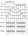
- FIG. 5 shows a driving method for a liquid crystal display according to a first embodiment of the present invention. Such a driving method will be described in conjunction with the liquid crystal display shown in FIG. 1 .
- a sequence of control signals Cs is converted every horizontal period.
- demultiplexors DEMUX 1 to DEMUXk reverse-sequentially supply four data to data lines DL 1 to DLn.
- the gate scanning signal GSS is applied to a third gate line GL 3
- the demultiplexors DEMUX 1 to DEMUXk sequentially supply four data to the data lines DL 1 to DLn.
- the first to fourth control signals CS 1 to CS 4 are reverse-sequentially applied to the demultiplexors DEMUX 1 to DEMUXk.
- the fourth MOS transistor MN 4 is turned on in a time interval when the fourth control signal CS 4 has a high state, to thereby apply a green data signal G 3 from the data D-IC 12 to the eighth data line DL 8 .
- the third demultiplexor DEMUX 3 is supplied with the third control signal CS 3 .
- the third MOS transistor MN 3 is turned on in a time interval when the third control signal CS 3 has a high state, to thereby a red data signal R 3 from the D-IC 12 to the seventh data line DL 7 .
- the green data signal G 3 charged in the eighth data line DL 8 by the coupling capacitor between the seventh and eighth data lines DL 8 and DL 7 is changed by the red data signal R 3 applied to the seventh data line DL 7 .
- the second demultiplexor DEMUX 2 is supplied with the second control signal CS 2 .
- the second MOS transistor MN 2 is turned on, to thereby apply a blue data signal B 2 from the data D-IC to the sixth data line DL 6 .
- the red data signal R 3 charged in the seventh data line DL 7 by the coupling capacitor Cc between the seventh and sixth data lines DL 7 and DL 6 is changed by the blue data signal B 2 applied to the sixth data line DL 6 .
- the first demultiplexor DEMUX 1 is supplied with the first control signal CS 1 .
- the first MOS control signal is turned on, to thereby apply a green data signal from the data D-IC 12 to the fifth data line DL 5 .
- the blue data signal B 2 charged in the sixth data line DL 6 by the coupling capacitor Cc between the sixth and fifth data lines DL 6 and DL 5 is changed by the green data signal G 2 applied to the fifth data line DL 5 .
- the green data signal G 3 charged in the eighth data line DL 8 also is changed by a blue data signal B 3 applied to the ninth data line DL 9 .
- the control signals CS 1 to CS 4 are reverse-sequentially applied, the data signal applied to the eighth data line DL 8 is changed twice while the data signals applied to the seventh and sixth data lines DL 7 and DL 6 are changed once.
- the data signal applied to the fifth data line DL 5 is not changed.
- the gate scanning signal GSS is applied to the third gate line GL 3 .
- the first to fourth control signals CS 1 to CS 4 are sequentially applied to the demultiplexors DEMUX 1 to DEMUXk. If the control signals CS 1 to CS 4 are sequentially applied, then the data signal applied to the fifth data line DL 5 is changed twice as mentioned above. The data signals applied to the sixth and seventh data lines DL 6 and DL 7 are changed once. On the other hand, the data signal applied to the eighth data line DL 8 is not changed.
- the liquid crystal display according to the first embodiment of the present invention can obtain a visually uniform picture.
- FIG. 6A shows a leakage current generated at the data line when a control signal is sequentially applied.
- the first data line DL 1 receives a first red data signal R 1 from the first MOS transistor MN 1 of the first demultiplexor DEMUX 1 in a time interval when the first control signal CS 1 has a high state.
- the first data line DL 1 maintains the charged voltage until the falling edge of the gate scanning signal GSS.
- a voltage charged in the first data line DL 1 is leaked for a long time from the falling edge of the first control signal CS 1 until the falling edge of the gate scanning signal GSS.
- the first data line DL 1 applies a voltage signal lower than the initially received red data signal R 1 to the pixel.
- a voltage applied to the first data line DL 1 is leaked by a voltage ⁇ V 1 .
- the fourth data line DL 4 receives the second red data signal R 2 from the fourth MOS transistor MN 4 of the first demultiplexor DEMUX 1 in a time interval when the fourth control signal CS 4 has a high state.
- the fourth data line DL 4 maintains the charged voltage until the falling edge of the gate scanning signal GSS.
- the voltage charged in the fourth data line DL 4 is leaked for a short time from the falling edge of the fourth control signal CS 4 until the falling edge of the gate scanning signal GSS.
- a voltage applied to the fourth data line DL 4 is leaked by a voltage ⁇ V 2 .
- the present liquid crystal display has an averagely uniform leakage voltage, so that it can obtain a visually uniform picture.
- FIG. 7 A and FIG. 7B are waveform diagrams for showing a driving method according to a second embodiment of the present invention.
- a sequence of the control signals CS 1 to CS 4 is changed every frame.
- the control signals CS 1 to CS 4 are sequentially applied in the first and fourth frames while being reverse-sequentially applied in the second and third frames. Accordingly, a change frequency of the data signal applied to the data lines DL 1 to DLn and a leakage current becomes uniform averagely, thereby obtaining a visually uniform picture.
- the setting of a conversion frequency of the control signals CS 1 to CS 4 to four frames in the second embodiment of the present invention aims to prevent a generation of a direct current offset voltage from each pixel. In other words, when the liquid crystal display panel 10 is driven in a dot inversion, each data line DL 1 to DLn is alternately supplied with a data signal having positive and negative voltage levels.
- a positive red data signal +R is applied to the first data line DL 1 in a certain horizontal period
- a negative green data signal ⁇ G is applied to the second data line DL 2 .
- a negative red data signal ⁇ R is applied to the first data line DL 1 while a positive green data signal +G is applied to the second data line DL 2 .
- control signals CS 1 to CS 4 may be reverse-sequentially applied in the first and fourth frames while being sequentially applied in the third and fourth frames.
- control signals are sequentially and reverse-sequentially applied to the demultiplexors alternately every frame or every horizontal period. Accordingly, a voltage level of the data line and a conversion frequency of the data signal become averagely uniform, to thereby obtain a uniform picture.
Applications Claiming Priority (2)
| Application Number | Priority Date | Filing Date | Title |
|---|---|---|---|
| KR2000-31462 | 2000-06-08 | ||
| KR10-2000-0031462A KR100367010B1 (ko) | 2000-06-08 | 2000-06-08 | 액정표시장치 및 그 구동방법 |
Publications (2)
| Publication Number | Publication Date |
|---|---|
| US20010050665A1 US20010050665A1 (en) | 2001-12-13 |
| US7084844B2 true US7084844B2 (en) | 2006-08-01 |
Family
ID=19671444
Family Applications (1)
| Application Number | Title | Priority Date | Filing Date |
|---|---|---|---|
| US09/874,960 Expired - Lifetime US7084844B2 (en) | 2000-06-08 | 2001-06-07 | Liquid crystal display and driving method thereof |
Country Status (2)
| Country | Link |
|---|---|
| US (1) | US7084844B2 (ko) |
| KR (1) | KR100367010B1 (ko) |
Cited By (11)
| Publication number | Priority date | Publication date | Assignee | Title |
|---|---|---|---|---|
| US20050024297A1 (en) * | 2003-07-30 | 2005-02-03 | Dong-Yong Shin | Display and driving method thereof |
| US20050041488A1 (en) * | 2003-07-22 | 2005-02-24 | Seiko Epson Corporation | Electro-optical device, method for driving the electro-optical device, and electronic apparatus including the electro-optical device |
| US20050219276A1 (en) * | 2004-03-31 | 2005-10-06 | Nec Electronics Corporation | Method and apparatus for display panel drive |
| US20060187162A1 (en) * | 2005-01-31 | 2006-08-24 | Kabushiki Kaisha Toshiba | Plain display apparatus, display control circuit and display control method |
| US20070171165A1 (en) * | 2006-01-25 | 2007-07-26 | Ching-Yun Chuang | Devices and methods for controlling timing sequences for displays of such devices |
| US20080088558A1 (en) * | 2002-12-31 | 2008-04-17 | Mun-Chul Kim | Driving circuit for use in cholesteric liquid crystal display device |
| US20100117939A1 (en) * | 2008-11-07 | 2010-05-13 | An-Su Lee | Organic light emitting display device |
| US20150248855A1 (en) * | 2014-03-03 | 2015-09-03 | Samsung Display Co., Ltd. | Organic light emitting display device |
| WO2016101309A1 (zh) * | 2014-12-24 | 2016-06-30 | 深圳市华星光电技术有限公司 | 液晶面板的驱动电路及液晶显示装置 |
| US9466255B2 (en) | 2012-02-28 | 2016-10-11 | Samsung Display Co., Ltd. | Display apparatus and method of driving the same |
| US11769458B2 (en) * | 2019-05-14 | 2023-09-26 | Samsung Display Co., Ltd. | Display device and method of driving the same |
Families Citing this family (29)
| Publication number | Priority date | Publication date | Assignee | Title |
|---|---|---|---|---|
| KR100464208B1 (ko) * | 2001-12-20 | 2005-01-03 | 엘지.필립스 엘시디 주식회사 | 액정 표시장치 및 그 구동방법 |
| KR100894644B1 (ko) | 2002-12-03 | 2009-04-24 | 엘지디스플레이 주식회사 | 액정표시장치의 데이터 구동 장치 및 방법 |
| KR100894643B1 (ko) * | 2002-12-03 | 2009-04-24 | 엘지디스플레이 주식회사 | 액정표시장치의 데이터 구동 장치 및 방법 |
| KR100905330B1 (ko) * | 2002-12-03 | 2009-07-02 | 엘지디스플레이 주식회사 | 액정표시장치의 데이터 구동 장치 및 방법 |
| KR100581800B1 (ko) * | 2004-06-07 | 2006-05-23 | 삼성에스디아이 주식회사 | 유기 전계발광 표시 장치 및 역다중화부 |
| KR100604054B1 (ko) * | 2004-10-13 | 2006-07-24 | 삼성에스디아이 주식회사 | 발광 표시장치 |
| US20070103421A1 (en) * | 2004-11-05 | 2007-05-10 | Nec Corporation | Liquid-crystal display, projector system, portable terminal unit, and method of driving liquid-crystal display |
| US20070030237A1 (en) * | 2005-08-08 | 2007-02-08 | Toppoly Optoelectronics Corp. | Source driving method and source driver for liquid crystal display device |
| US7576724B2 (en) * | 2005-08-08 | 2009-08-18 | Tpo Displays Corp. | Liquid crystal display device and electronic device |
| KR100630759B1 (ko) * | 2005-08-16 | 2006-10-02 | 삼성전자주식회사 | 멀티 채널 - 싱글 앰프 구조를 갖는 액정 표시 장치의 구동방법 |
| EP1964100B1 (en) * | 2005-12-16 | 2011-04-20 | Trident Microsystems (Far East) Ltd. | Apparatus and method for color shift compensation in displays |
| WO2007069205A2 (en) * | 2005-12-16 | 2007-06-21 | Koninklijke Philips Electronics N.V. | Apparatus and method for color shift compensation in displays |
| KR20080057501A (ko) * | 2006-12-20 | 2008-06-25 | 삼성전자주식회사 | 액정표시장치 및 이의 구동방법 |
| KR100896045B1 (ko) * | 2007-06-26 | 2009-05-11 | 엘지전자 주식회사 | 유기전계발광표시장치 |
| KR101469033B1 (ko) | 2008-01-08 | 2014-12-04 | 삼성디스플레이 주식회사 | 액정표시장치 및 그 제어방법 |
| KR101420443B1 (ko) * | 2008-12-23 | 2014-07-16 | 엘지디스플레이 주식회사 | 액정표시장치 |
| TWI397051B (zh) * | 2008-12-25 | 2013-05-21 | Himax Tech Ltd | 降低功率消耗之液晶顯示器裝置及其驅動方法 |
| KR102034236B1 (ko) * | 2013-01-17 | 2019-10-21 | 삼성디스플레이 주식회사 | 유기전계발광 표시장치 |
| KR102211694B1 (ko) * | 2014-07-17 | 2021-02-04 | 삼성디스플레이 주식회사 | 발광소자 표시장치 및 이의 구동 방법 |
| CN104867452A (zh) * | 2015-06-08 | 2015-08-26 | 深圳市华星光电技术有限公司 | 信号分离器及amoled显示装置 |
| CN105096867B (zh) * | 2015-08-07 | 2018-04-10 | 深圳市华星光电技术有限公司 | 一种液晶显示器及其控制方法 |
| KR102345665B1 (ko) * | 2015-09-07 | 2022-01-03 | 삼성디스플레이 주식회사 | 표시장치 및 그의 구동방법 |
| CN105676051A (zh) * | 2016-01-21 | 2016-06-15 | 北京荣达千里科技有限公司 | 一种集成线序测试装置和方法 |
| KR20180059664A (ko) * | 2016-11-25 | 2018-06-05 | 엘지디스플레이 주식회사 | 표시장치 |
| KR102578713B1 (ko) * | 2016-11-29 | 2023-09-18 | 엘지디스플레이 주식회사 | 표시장치 |
| CN108831391A (zh) * | 2018-06-21 | 2018-11-16 | 深圳市华星光电半导体显示技术有限公司 | 一种液晶显示面板的驱动电路及液晶显示器 |
| CN110299109B (zh) * | 2019-06-27 | 2022-09-20 | 敦泰电子有限公司 | 平面显示器、穿戴式装置以及平面显示器的驱动方法 |
| JP7434913B2 (ja) | 2020-01-16 | 2024-02-21 | セイコーエプソン株式会社 | 回路装置、電気光学装置及び電子機器 |
| CN111477180B (zh) * | 2020-04-21 | 2024-04-12 | 京东方科技集团股份有限公司 | 一种显示面板及其驱动方法、显示装置 |
Citations (6)
| Publication number | Priority date | Publication date | Assignee | Title |
|---|---|---|---|---|
| US5168270A (en) * | 1990-05-16 | 1992-12-01 | Nippon Telegraph And Telephone Corporation | Liquid crystal display device capable of selecting display definition modes, and driving method therefor |
| US5192945A (en) * | 1988-11-05 | 1993-03-09 | Sharp Kabushiki Kaisha | Device and method for driving a liquid crystal panel |
| KR20000023298A (ko) | 1998-09-21 | 2000-04-25 | 니시무로 타이죠 | 평면표시장치 |
| US6097362A (en) * | 1997-10-14 | 2000-08-01 | Lg Semicon Co., Ltd. | Driver for liquid crystal display |
| US6333729B1 (en) * | 1997-07-10 | 2001-12-25 | Lg Electronics Inc. | Liquid crystal display |
| US6424328B1 (en) * | 1998-03-19 | 2002-07-23 | Sony Corporation | Liquid-crystal display apparatus |
-
2000
- 2000-06-08 KR KR10-2000-0031462A patent/KR100367010B1/ko active IP Right Grant
-
2001
- 2001-06-07 US US09/874,960 patent/US7084844B2/en not_active Expired - Lifetime
Patent Citations (6)
| Publication number | Priority date | Publication date | Assignee | Title |
|---|---|---|---|---|
| US5192945A (en) * | 1988-11-05 | 1993-03-09 | Sharp Kabushiki Kaisha | Device and method for driving a liquid crystal panel |
| US5168270A (en) * | 1990-05-16 | 1992-12-01 | Nippon Telegraph And Telephone Corporation | Liquid crystal display device capable of selecting display definition modes, and driving method therefor |
| US6333729B1 (en) * | 1997-07-10 | 2001-12-25 | Lg Electronics Inc. | Liquid crystal display |
| US6097362A (en) * | 1997-10-14 | 2000-08-01 | Lg Semicon Co., Ltd. | Driver for liquid crystal display |
| US6424328B1 (en) * | 1998-03-19 | 2002-07-23 | Sony Corporation | Liquid-crystal display apparatus |
| KR20000023298A (ko) | 1998-09-21 | 2000-04-25 | 니시무로 타이죠 | 평면표시장치 |
Cited By (21)
| Publication number | Priority date | Publication date | Assignee | Title |
|---|---|---|---|---|
| US20080088558A1 (en) * | 2002-12-31 | 2008-04-17 | Mun-Chul Kim | Driving circuit for use in cholesteric liquid crystal display device |
| US7656379B2 (en) * | 2002-12-31 | 2010-02-02 | Lg Display Co., Ltd. | Driving circuit for use in cholesteric liquid crystal display device |
| US20050041488A1 (en) * | 2003-07-22 | 2005-02-24 | Seiko Epson Corporation | Electro-optical device, method for driving the electro-optical device, and electronic apparatus including the electro-optical device |
| US8243057B2 (en) * | 2003-07-30 | 2012-08-14 | Samsung Mobile Display Co., Ltd. | Display and driving method thereof |
| US20050024297A1 (en) * | 2003-07-30 | 2005-02-03 | Dong-Yong Shin | Display and driving method thereof |
| US7545394B2 (en) * | 2004-03-31 | 2009-06-09 | Nec Electronics Corporation | Method and drive sequence for time-divisionally driving a display panel |
| US20050219276A1 (en) * | 2004-03-31 | 2005-10-06 | Nec Electronics Corporation | Method and apparatus for display panel drive |
| US20060187162A1 (en) * | 2005-01-31 | 2006-08-24 | Kabushiki Kaisha Toshiba | Plain display apparatus, display control circuit and display control method |
| US7595793B2 (en) * | 2005-01-31 | 2009-09-29 | Kabushiki Kaisha Toshiba | Plain display apparatus, display control circuit and display control method, that divide plural signal lines in blocks |
| US20070171165A1 (en) * | 2006-01-25 | 2007-07-26 | Ching-Yun Chuang | Devices and methods for controlling timing sequences for displays of such devices |
| US20100117939A1 (en) * | 2008-11-07 | 2010-05-13 | An-Su Lee | Organic light emitting display device |
| US8373626B2 (en) * | 2008-11-07 | 2013-02-12 | Samsung Display Co., Ltd. | Organic light emitting display device having demultiplexers |
| US9466255B2 (en) | 2012-02-28 | 2016-10-11 | Samsung Display Co., Ltd. | Display apparatus and method of driving the same |
| US20150248855A1 (en) * | 2014-03-03 | 2015-09-03 | Samsung Display Co., Ltd. | Organic light emitting display device |
| US9672767B2 (en) * | 2014-03-03 | 2017-06-06 | Samsung Display Co., Ltd. | Organic light emitting display device |
| US20160189640A1 (en) * | 2014-12-24 | 2016-06-30 | Shenzhen China Star Optoelectronics Technology Co. Ltd. | Driving circuits of liquid crystal panel and liquid crystal devices |
| WO2016101309A1 (zh) * | 2014-12-24 | 2016-06-30 | 深圳市华星光电技术有限公司 | 液晶面板的驱动电路及液晶显示装置 |
| US9672776B2 (en) * | 2014-12-24 | 2017-06-06 | Shenzhen China Star Optoelectronics Technology Co., Ltd | Driving circuits of liquid crystal panel and liquid crystal devices |
| GB2547576A (en) * | 2014-12-24 | 2017-08-23 | Shenzhen China Star Optoelect | Drive circuit of liquid crystal panel and liquid crystal display device |
| GB2547576B (en) * | 2014-12-24 | 2021-08-18 | Shenzhen China Star Optoelect | Driving circuits of liquid crystal panel and liquid crystal devices |
| US11769458B2 (en) * | 2019-05-14 | 2023-09-26 | Samsung Display Co., Ltd. | Display device and method of driving the same |
Also Published As
| Publication number | Publication date |
|---|---|
| KR100367010B1 (ko) | 2003-01-09 |
| KR20010110848A (ko) | 2001-12-15 |
| US20010050665A1 (en) | 2001-12-13 |
Similar Documents
| Publication | Publication Date | Title |
|---|---|---|
| US7084844B2 (en) | Liquid crystal display and driving method thereof | |
| US8294655B2 (en) | Display drive device and display apparatus having same | |
| US7808472B2 (en) | Liquid crystal display and driving method thereof | |
| US9135878B2 (en) | Shift register and liquid crystal display device using the same | |
| US7812805B2 (en) | Driver circuit and display device | |
| US7221344B2 (en) | Liquid crystal display device and driving control method thereof | |
| US7212183B2 (en) | Liquid crystal display apparatus having pixels with low leakage current | |
| US7505017B1 (en) | Method of driving liquid crystal display | |
| US20060097977A1 (en) | Liquid crystal display device | |
| US8416175B2 (en) | Liquid crystal display device and method for driving the same | |
| JP2006139248A (ja) | 液晶表示装置及びその駆動方法 | |
| US8102385B2 (en) | Driving circuit of liquid crystal display device and method for driving the same | |
| US20070229429A1 (en) | Liquid crystal display device and driving method thereof | |
| US20070063949A1 (en) | Driving circuit, electro-optic device, and electronic device | |
| JP2008185993A (ja) | 電気光学装置、処理回路、処理方法およびプロジェクタ | |
| JPH06138440A (ja) | 表示装置及びその駆動方法 | |
| KR20070098365A (ko) | 액정표시장치의 감마보정전압 보상회로 | |
| JPH11161237A (ja) | 液晶表示装置 | |
| KR100965587B1 (ko) | 액정표시장치 및 이의 구동방법 | |
| TWI287213B (en) | Correction method of image signal, correction circuit, photoelectric device and electronic device | |
| WO2007052421A1 (ja) | 表示装置、データ信号線駆動回路、および表示装置の駆動方法 | |
| KR100998119B1 (ko) | 액정표시장치 | |
| KR100971390B1 (ko) | 감마 기준 전압 발생 회로 | |
| JP2006099034A (ja) | 電気光学装置の調整方法および調整装置 | |
| US20040207591A1 (en) | Method and circuit for driving liquid crystal display |
Legal Events
| Date | Code | Title | Description |
|---|---|---|---|
| AS | Assignment |
Owner name: LG. PHILIPS LCD CO., LTD., KOREA, REPUBLIC OF Free format text: ASSIGNMENT OF ASSIGNORS INTEREST;ASSIGNORS:YEO, JU CHUN;KIM, SEONG GYUN;REEL/FRAME:011881/0031 Effective date: 20010601 |
|
| FEPP | Fee payment procedure |
Free format text: PAYOR NUMBER ASSIGNED (ORIGINAL EVENT CODE: ASPN); ENTITY STATUS OF PATENT OWNER: LARGE ENTITY |
|
| STCF | Information on status: patent grant |
Free format text: PATENTED CASE |
|
| AS | Assignment |
Owner name: LG DISPLAY CO., LTD., KOREA, REPUBLIC OF Free format text: CHANGE OF NAME;ASSIGNOR:LG. PHILIPS LCD CO., LTD.;REEL/FRAME:021773/0029 Effective date: 20080304 Owner name: LG DISPLAY CO., LTD.,KOREA, REPUBLIC OF Free format text: CHANGE OF NAME;ASSIGNOR:LG. PHILIPS LCD CO., LTD.;REEL/FRAME:021773/0029 Effective date: 20080304 |
|
| FEPP | Fee payment procedure |
Free format text: PAYER NUMBER DE-ASSIGNED (ORIGINAL EVENT CODE: RMPN); ENTITY STATUS OF PATENT OWNER: LARGE ENTITY |
|
| FPAY | Fee payment |
Year of fee payment: 4 |
|
| FPAY | Fee payment |
Year of fee payment: 8 |
|
| MAFP | Maintenance fee payment |
Free format text: PAYMENT OF MAINTENANCE FEE, 12TH YEAR, LARGE ENTITY (ORIGINAL EVENT CODE: M1553) Year of fee payment: 12 |