US7023542B2 - Imaging method and apparatus - Google Patents
Imaging method and apparatus Download PDFInfo
- Publication number
- US7023542B2 US7023542B2 US10/115,533 US11553302A US7023542B2 US 7023542 B2 US7023542 B2 US 7023542B2 US 11553302 A US11553302 A US 11553302A US 7023542 B2 US7023542 B2 US 7023542B2
- Authority
- US
- United States
- Prior art keywords
- transparent medium
- defects
- light
- image
- lens
- Prior art date
- Legal status (The legal status is an assumption and is not a legal conclusion. Google has not performed a legal analysis and makes no representation as to the accuracy of the status listed.)
- Expired - Lifetime, expires
Links
- 238000003384 imaging method Methods 0.000 title claims abstract description 32
- 230000003287 optical effect Effects 0.000 claims abstract description 66
- 238000000034 method Methods 0.000 claims abstract description 43
- 230000007547 defect Effects 0.000 claims description 64
- 238000003491 array Methods 0.000 claims description 13
- 238000004458 analytical method Methods 0.000 claims description 7
- 238000009792 diffusion process Methods 0.000 claims description 7
- 239000011521 glass Substances 0.000 claims description 6
- 238000001914 filtration Methods 0.000 claims description 5
- 239000000835 fiber Substances 0.000 claims description 3
- 239000010408 film Substances 0.000 description 13
- 238000007689 inspection Methods 0.000 description 6
- 238000004519 manufacturing process Methods 0.000 description 6
- 230000008901 benefit Effects 0.000 description 4
- 230000008569 process Effects 0.000 description 4
- 238000001514 detection method Methods 0.000 description 3
- 239000000463 material Substances 0.000 description 3
- 239000002245 particle Substances 0.000 description 3
- 238000007796 conventional method Methods 0.000 description 2
- 230000005670 electromagnetic radiation Effects 0.000 description 2
- 238000012986 modification Methods 0.000 description 2
- 230000004048 modification Effects 0.000 description 2
- 239000012788 optical film Substances 0.000 description 2
- 239000004065 semiconductor Substances 0.000 description 2
- 230000035945 sensitivity Effects 0.000 description 2
- 238000000149 argon plasma sintering Methods 0.000 description 1
- 230000005540 biological transmission Effects 0.000 description 1
- 230000008859 change Effects 0.000 description 1
- 239000002537 cosmetic Substances 0.000 description 1
- 230000001419 dependent effect Effects 0.000 description 1
- 230000007246 mechanism Effects 0.000 description 1
- 229910044991 metal oxide Inorganic materials 0.000 description 1
- 150000004706 metal oxides Chemical class 0.000 description 1
- 239000000203 mixture Substances 0.000 description 1
- 229920000642 polymer Polymers 0.000 description 1
- 238000007619 statistical method Methods 0.000 description 1
Images


Classifications
-
- G—PHYSICS
- G01—MEASURING; TESTING
- G01N—INVESTIGATING OR ANALYSING MATERIALS BY DETERMINING THEIR CHEMICAL OR PHYSICAL PROPERTIES
- G01N21/00—Investigating or analysing materials by the use of optical means, i.e. using sub-millimetre waves, infrared, visible or ultraviolet light
- G01N21/84—Systems specially adapted for particular applications
- G01N21/88—Investigating the presence of flaws or contamination
- G01N21/89—Investigating the presence of flaws or contamination in moving material, e.g. running paper or textiles
- G01N21/892—Investigating the presence of flaws or contamination in moving material, e.g. running paper or textiles characterised by the flaw, defect or object feature examined
- G01N21/896—Optical defects in or on transparent materials, e.g. distortion, surface flaws in conveyed flat sheet or rod
-
- G—PHYSICS
- G01—MEASURING; TESTING
- G01N—INVESTIGATING OR ANALYSING MATERIALS BY DETERMINING THEIR CHEMICAL OR PHYSICAL PROPERTIES
- G01N21/00—Investigating or analysing materials by the use of optical means, i.e. using sub-millimetre waves, infrared, visible or ultraviolet light
- G01N21/84—Systems specially adapted for particular applications
- G01N21/88—Investigating the presence of flaws or contamination
- G01N21/89—Investigating the presence of flaws or contamination in moving material, e.g. running paper or textiles
Definitions
- the present invention relates to an imaging method and apparatus ideally suited for analyzing the optical quality of at least a portion of a transparent medium, more particularly the invention superimposing multiple images to analyze the quality of a transparent medium, for example, to detect refracting, obstructing and scattering defects.
- Line scan cameras that are capable of detecting scattering defects such as scratches or surface particles.
- the line scan cameras are configured with dark-field optics in either reflected or transmitted mode and are capable of detecting the noted defects.
- this single configuration is not sufficient for detecting refracting defects or embedded particles that do not distort the surface of film.
- Laser scanners can be configured with multiple channels in order to be sensitive to all defects at the same time. Basically, this is the same as having multiple systems, one for each channel, which increases the system complexity and cost. Also, laser scanners are large, complex electromechanical systems that are expensive to implement in production environments. Laser scanners are also difficult to run in parallel for inspection applications requiring extremely high resolution across wide webs.
- schlieren imaging Another imaging technique is referred to as schlieren imaging. This technique is generally useful for measuring variations in the refractive index within an optical system. The technique detects inhomogeneities within a medium by detecting the energy refracted by that portion of the medium in which the inhomogeneity occurs. Schlieren imaging is generally used over long distances with large objects. The system is not suitable for film inspection because it is only capable if detecting changes in the refractive index of the medium.
- the present invention is directed to an imaging apparatus and method for detecting anomalies and quantifying optical properties of transparent media.
- the present invention superimposes, either optically or electronically, at least two images of the transparent media in order to obtain optical properties of at a least a portion of the transparent medium.
- the method for characterizing the optical properties of a transparent media includes transmitting light from a point light source two times through the transparent medium.
- the light is directed through a lens onto a detector array to form an image of the transparent medium.
- At least one converging mirror is utilized to direct light to a point at a position substantially near the optical center of the lens.
- the image is then analyzed using conventional analytical techniques to characterize the optical properties of the transparent medium.
- the combined distance between the point light source to the converging mirror and from the converging mirror to the detector array is about four times the focal length of the mirror.
- a method for characterizing transparent media involves superimposing two or more images of a transparent medium wherein each image is generated by reflecting light emitted from a point light source off a converging mirror. The light converges to a single point substantially near the center of a lens. The light is transmitted through the transparent medium either before or after reflecting from the mirror. Two or more images are formed, each having unique focal planes, such that one of the unique focal planes corresponds to the transparent medium.
- the images may be superimposed through the use of a single lens onto a detector array. Alternatively, the images may be formed using two or more lenses with separate detector arrays, and the corresponding signals from the detector arrays superimposed electronically.
- the apparatus of the present invention generally includes a point light source for transmitting light through a transparent medium.
- a converging mirror is provided for reflecting the light back through the transparent medium to a point at a position substantially near the optical center of the lens.
- a detector array receives an image from the lens. The image is analyzed in an analyzing device to determine optical properties of said transparent medium.
- a preferred embodiment of the apparatus of the present invention superimposes two or more images of a transparent medium.
- the apparatus includes one or more imaging systems. Each system has a point light source for transmitting light through a transparent medium and a converging mirror positioned such that light from the point light source converges to a point substantially near a center of an imaging lens.
- a detector array is included in the apparatus for receiving an image from the lens. Each system generates an image and each image has unique focal planes, such that one of the unique focal planes corresponds to the transparent medium.
- the embodiments of the present invention are capable of characterizing optical characteristics in the transparent medium such as, for example, defects, non-uniformities, and variations in clarity, optical density, or diffusion.
- the method of the present invention is capable of detecting optical defects including refracting defects, scattering defects, and obstructing defects with a single configuration.
- web means a sheet of material having a dimensional width in one direction and indeterminate length in the orthogonal direction;
- “converging mirror” means a mirror configured specifically such that light emitted from a single point is directed back to a single point after reflection from the mirror surface;
- imaged line on web means a portion of the web which is currently being imaged onto the detector array
- point light source means a source of electromagnetic radiation with the physical form of a single point
- beamsplitter means an optical device that uses a mirror or prisms to divide a light beam into two or more paths;
- “lens” means an object or group of objects that bend light rays causing them to converge or diverge to create an image
- “camera” means a wide variety of devices through which light from an object is focused onto a light-sensitive material, such as film or semiconductor devices, in order to record the image; and
- detector array means an array of photosensitive devices capable of converting incoming light photons into an electrical signal.
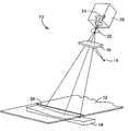
- FIG. 1 is an isometric view of one embodiment of the present invention
- FIG. 2 is an isometric view of the embodiment of FIG. 1 in an unfolded array
- FIG. 3 is an isometric view of another embodiment of the present invention.
- FIGS. 4 a, and 4 b are images of a various types of defects that may be detected through use of the present invention.
- FIG. 5 is an isometric view of an alternative embodiment of the present invention.
- the present invention is suitable for determining optical properties of a transparent medium.
- the invention provides mechanisms for superimposing two or more images of at least a portion of the transparent medium. The images are superimposed either optically or electronically in order to determine the optical characteristics of the transparent medium.
- FIG. 1 depicts one embodiment of the apparatus and method of the present invention.
- the imaging system 10 is suitable for imaging optical properties of a transparent medium 12 .
- the imaging system 10 includes a point light source 14 that directs light onto beam splitter 16 .
- the light is transmitted through the transparent medium 12 and onto a converging mirror 18 .
- the light is then reflected back through the transparent medium 12 through the same line or area as the first pass of light. This line or area is referred to as the imaged area 20 .
- the light reflected from the converging mirror and passing through the imaged area 20 for the second time is directed to the lens 22 .
- the light from the converging mirror 18 is directed to a point on the lens 22 at a position substantially near the optical center of lens 22 .
- a detector array 24 residing in camera 26 , receives the light from the lens and forms electrical signals corresponding to the imaged area 20 of transparent medium 12 .
- the electrical signals from the detector array representing the image of transparent medium may then be processed or analyzed using conventionally recognized techniques.
- FIG. 2 is provided to further illustrate, in an unfolded view, the embodiment of FIG. 1 .
- the light from point light source 14 fans out from the point light source 14 and through the transparent medium 12 until it reflects from the converging mirror 18 .
- the reflected light passes back through web 12 for a second time and converges to a single point.
- the point at which the light converges after reflecting from the converging mirror 18 is a point substantially near the optical center of lens 22 .
- An image of the web is provided by the detector array 24 from the light passing through the lens 22 .
- the present invention is suitable for imaging optical properties of a transparent medium.
- a transparent medium may be any material that is capable of allowing at least some transmission of light with no appreciable scattering or diffusion.
- the transparent medium is selected from polymeric films, glass, coated films or coated glass.
- the transparent medium may be preferably provided in either web form or as discrete parts. In the case of web imaging, the web may be traveling at a predetermined speed while the present invention is providing images of continuous segments or an imaged area of the web as the web travels through the area highlighted by the point light source.
- optical properties of the transparent medium may involve such characteristics as defects, caliper, non-uniformities, clarity, optical density, diffusion or combinations of these noted characteristics.
- the present invention is capable of imaging the transparent medium to determine variations of one or all of the noted properties from a desired standard.
- Conventional imaging systems are not capable of addressing various types of defects in a single configuration.
- conventional configurations are not capable of detecting refracting defects while simultaneously detecting other defects such as scattering defects or obstructing defects.
- the ability of the present invention to simultaneously image at least two views of the same section of imaged medium enables inspection of the medium for such optical properties as refracting defects, scattering defects, obstructing defects or combinations thereof in a single configuration.
- a point light source is utilized to transmit electromagnetic radiation.
- the point light source is selected to provide sufficient energy so that the detector array records an image of the transparent medium.
- Those skilled in the art are capable of selecting a point light source to match specific detector arrays. All conventionally recognized point light sources are suitable for use with the present invention.
- Non-limiting examples of point light sources may include incandescent lamps, fiber optic light or light emitting diodes.
- an aperture may be used to limit the effective size of the source. Typical aperture sizes range from 100 ⁇ m to 5 mm.
- a beam splitter is utilized to divide a light beam into two or more paths.
- Beam splitters may be employed in various alignments to provide coaxial lighting. Coaxial lighting may assist in reducing the occurrence of single features represented twice on a single image, also referred to as ghosting.
- Conventional beam splitters are suitable for use with the present invention.
- a converging mirror employed in practicing the present invention, is configured specifically such that light emitted from the point light source is directed back to a point after reflecting from the mirror surface.
- the converging mirror directs light to a point at a position near the optical center of the lens.
- the converging mirror may be converging in at least one dimension and preferably two dimensions.
- the type of converging mirror employed affects the imaging system's sensitivity. Certain forms of transparent media and specific types of optical properties require higher quality mirrors in order to appropriately image specific optical properties. Those skilled in the art are capable of matching mirror quality to achieve the level of imaging needed for specific transparent films.
- the present invention may also employ flat mirrors to fold the optical path, thereby drastically reducing physical space requirements for the inventive apparatus.
- a lens is employed in the method and apparatus of the present invention.
- the lens bends light rays, causing them to converge and create an image on the detector array. It serves to map a physical section of the transparent media to corresponding positions on the detector array.
- the lens is preferably focused on a plane corresponding to the position of the transparent medium.
- the detector array is an array of photosensitive devices capable of converting incoming light photons into electrical signals.
- the lens forms an image on the detector array.
- the detector array converts image intensity to corresponding electrical signal amplitude.
- the signal created by the detector array is an electronic representation of the optical image transmitted by the lens.
- Conventional detector arrays generally recognized by those skilled in the art are suitable for use with the present invention.
- acceptable detector arrays may include either one-dimensional or two-dimensional arrays of a charge coupled device (CCD), a complimentary metal oxide semiconductor (CMOS) or photodiodes.
- CCD charge coupled device
- CMOS complimentary metal oxide semiconductor
- FIG. 1 The configuration of imaging system 10 is set up so that the combined distance from point light source 14 to converging mirror 18 and from the mirror to a convergence point near the center of lens 22 are about equal to four times the mirror's 18 focal length.
- FIG. 2 shows the two light paths unfolded.
- the distance from the point light source 14 to the mirror 18 is equal to the distance from the mirror 18 to the center of the lens 22 .
- the distances may be slightly unequal while still maintaining good convergence as long as the total distance remains substantially close to four times the mirror's 18 focal distance.
- a typical alignment procedure with the preferred embodiment is as follows. First, roughly align the beamsplitter 16 , converging mirror 18 , lens 22 , and camera 26 using conventional methods such that the center of the camera 26 , lens 22 , beamsplitter 16 , and converging mirror 18 are coaxial. Also, position the point light source 14 and lens 22 so that the total distance between them is 4 F as described above. Next, using the laser in place of the point light source 14 , fine-tune the beamsplitter 16 position until the beam exactly impacts the mirror's 18 center.
- FIG. 3 An alternative embodiment is illustrated in FIG. 3 .
- the imaging system 30 is set up to image the optical properties of transparent medium 32 .
- the point light source 34 is positioned relative to the converging mirror 38 such that all light rays will be reflected in parallel. This is referred to as telecentric imaging.
- the point light source emits light through beam splitter 36 .
- the light is transmitted to flat mirror 48 where it is directed to converging mirror 38 .
- the converging mirror 38 reflects the light in parallel through transparent medium 32 to create an imaged area 40 .
- the light reflects from a second flat mirror 50 and is transmitted back through transparent medium 32 , reflected from converging mirror 38 and flat mirror 48 to lens 42 .
- FIG. 3 exemplifies the situation where the light rays, when placed at the focal point of a parabolic mirror, impacts the web in exactly the same manner, are reflected from flat mirror, and travel back to the converging mirror where they are again converged to a single point in the center of the imaging lens.
- the imaging resolution with this embodiment depicted in FIG. 3 is highly dependent on the specific implementation. Typical resolutions useful for web or piece part inspection may range from 20 ⁇ m to 1 mm as imaged on the detector array. However, the method is capable at resolutions as low as 100 mm or as high as 1 ⁇ m. The only limitations are the size and accuracy of the converging mirror combined with the number of pixels and sensitivity of the sensor array.
- the image resulting from preferred embodiments actually consist of two superimposed images, one from each light pass through the transparent medium.
- the imaging plane of lens 14 is usually equal to the plane of the second pass.
- the first pass through the transparent medium 12 will not be in focus relative to the lens 22 .
- the image depicted in FIG. 4 a shows the relative contributions from each of the two passes.
- the first pass 52 accentuates subtle refracting defects 54 and is most effective if it is out of focus.
- the second pass 56 is then most sensitive to the light scattering 58 or obstructing defects 60 .
- FIG. 4 b shows a superposition of the two passes described in FIG. 4 a. It effectively captures the high frequency components related to small scattering defects 62 or obstructing defects 64 , such as scratches and particles, while also providing a strong optical signature for subtle refracting defects 66 such as polymer flows or caliper variations.
- an image After an image is captured, it must be analyzed to provide information about the optical properties of the transparent medium, such as, for example, defects.
- defects There are a variety of conventional methods to process the image to extract process variations.
- possible methods include, but are not limited to, spatial or frequency based filtering to enhance the defects followed by intensity level thresholding to binarize the image.
- intensity level thresholding to binarize the image.
- conventional blob analysis can be performed to extract and analyze the defects.
- uniformity analysis many different statistical analyses can be performed to quantify the variability of the image and thereby quantify the manufacturing process variability. As the process variability or defect level is quantified through this imaging technique, the results can then be used to improve and control the manufacturing process to increase and maintain high quality levels.
- the images of the transparent medium may be superimposed electronically as opposed to optically.
- FIG. 5 There are numerous alternative embodiments capable of producing similar benefits through the combination of independent single pass imaging systems.
- the first system 70 uses the focused lighting with the lens 72 focused in the plane of transparent medium 78 .
- the focal plane of lens 72 is depicted by arrow 84 . This corresponds to the second pass from the preferred embodiment.
- the point light source 74 is directed to a converging mirror 76 .
- the light is reflected from the converging mirror 76 through transparent medium 78 .
- the light passing through transparent medium 78 is directed to a point on the lens 72 substantially near the optical center of the lens 72 . This provides a first image on a detector array 80 located in camera 82 .
- the second system 90 uses the focused lighting from with the lens 92 focused before the plane of transparent medium 78 and corresponds to the first pass from the preferred embodiment.
- the focal plane of lens 92 is depicted by arrow 104 .
- the point light source 94 is directed through transparent medium 78 to a converging mirror 96 .
- the light is reflected from the converging mirror 96 to a point on the lens 92 substantially near the optical center of the lens 92 . This provides a second image on a detector array 100 located in camera 102 .
- the image output from the two detector arrays 80 , 100 are then superimposed electronically in a combining device 106 .
- combining devices include computers with multiple digital input channels or dedicated dyadic image processing hardware.
- the superimposed image of the optical characteristics of the transparent medium 78 may then be processed similar to that described in the preferred embodiment.
- Alternative embodiments such as that described with respect to FIG. 5 provide a desired level of flexibility because two or more imaging systems can be separately configured to enhance desired features.
Landscapes
- Engineering & Computer Science (AREA)
- Textile Engineering (AREA)
- Physics & Mathematics (AREA)
- Health & Medical Sciences (AREA)
- Life Sciences & Earth Sciences (AREA)
- Chemical & Material Sciences (AREA)
- Analytical Chemistry (AREA)
- Biochemistry (AREA)
- General Health & Medical Sciences (AREA)
- General Physics & Mathematics (AREA)
- Immunology (AREA)
- Pathology (AREA)
- Investigating Materials By The Use Of Optical Means Adapted For Particular Applications (AREA)
Priority Applications (7)
| Application Number | Priority Date | Filing Date | Title |
|---|---|---|---|
| US10/115,533 US7023542B2 (en) | 2002-04-03 | 2002-04-03 | Imaging method and apparatus |
| JP2003582529A JP2005528593A (ja) | 2002-04-03 | 2003-01-31 | 画像化方法および装置 |
| AU2003210779A AU2003210779A1 (en) | 2002-04-03 | 2003-01-31 | Imaging method and apparatus |
| PCT/US2003/002979 WO2003085389A1 (en) | 2002-04-03 | 2003-01-31 | Imaging method and apparatus |
| CNA038078430A CN1646895A (zh) | 2002-04-03 | 2003-01-31 | 成像方法及装置 |
| EP03745714A EP1493022A1 (en) | 2002-04-03 | 2003-01-31 | Imaging method and apparatus |
| KR10-2004-7015595A KR20040105831A (ko) | 2002-04-03 | 2003-01-31 | 화상 형성 방법 및 장치 |
Applications Claiming Priority (1)
| Application Number | Priority Date | Filing Date | Title |
|---|---|---|---|
| US10/115,533 US7023542B2 (en) | 2002-04-03 | 2002-04-03 | Imaging method and apparatus |
Publications (2)
| Publication Number | Publication Date |
|---|---|
| US20030189704A1 US20030189704A1 (en) | 2003-10-09 |
| US7023542B2 true US7023542B2 (en) | 2006-04-04 |
Family
ID=28673792
Family Applications (1)
| Application Number | Title | Priority Date | Filing Date |
|---|---|---|---|
| US10/115,533 Expired - Lifetime US7023542B2 (en) | 2002-04-03 | 2002-04-03 | Imaging method and apparatus |
Country Status (7)
| Country | Link |
|---|---|
| US (1) | US7023542B2 (enExample) |
| EP (1) | EP1493022A1 (enExample) |
| JP (1) | JP2005528593A (enExample) |
| KR (1) | KR20040105831A (enExample) |
| CN (1) | CN1646895A (enExample) |
| AU (1) | AU2003210779A1 (enExample) |
| WO (1) | WO2003085389A1 (enExample) |
Cited By (2)
| Publication number | Priority date | Publication date | Assignee | Title |
|---|---|---|---|---|
| WO2018045280A1 (en) * | 2016-09-01 | 2018-03-08 | 3M Innovative Properties Company | Machine direction line film inspection |
| US20190265385A1 (en) * | 2017-03-01 | 2019-08-29 | Omron Corporation | Photoelectric sensor |
Families Citing this family (11)
| Publication number | Priority date | Publication date | Assignee | Title |
|---|---|---|---|---|
| US7623699B2 (en) | 2004-04-19 | 2009-11-24 | 3M Innovative Properties Company | Apparatus and method for the automated marking of defects on webs of material |
| GB0503184D0 (en) * | 2005-02-16 | 2005-03-23 | Greenbank Terotech Ltd | A method and a device for generating data relating to particles in a particulate material |
| FR2892191B1 (fr) * | 2005-10-17 | 2008-04-04 | Vai Clecim Soc Par Actions Sim | Dispositif compact et procede d'inspection d'un produit en defilement, pour la detection automatique de defauts. |
| KR101442871B1 (ko) * | 2007-02-16 | 2014-09-19 | 쓰리엠 이노베이티브 프로퍼티즈 컴파니 | 시트 재료 조명 시스템 및 방법 |
| US7542821B2 (en) * | 2007-07-26 | 2009-06-02 | 3M Innovative Properties Company | Multi-unit process spatial synchronization of image inspection systems |
| US8175739B2 (en) * | 2007-07-26 | 2012-05-08 | 3M Innovative Properties Company | Multi-unit process spatial synchronization |
| US7797133B2 (en) * | 2008-09-10 | 2010-09-14 | 3M Innovative Properties Company | Multi-roller registered repeat defect detection of a web process line |
| CN102081047B (zh) * | 2009-11-27 | 2015-04-08 | 法国圣-戈班玻璃公司 | 用于对基板的缺陷进行区分的方法和系统 |
| JP6037701B2 (ja) * | 2012-08-03 | 2016-12-07 | 株式会社日立ハイテクノロジーズ | 免疫分析装置 |
| CN107688248A (zh) * | 2016-08-05 | 2018-02-13 | 豪威科技股份有限公司 | 硅基液晶测试平台 |
| US12305983B2 (en) * | 2020-06-17 | 2025-05-20 | Corning Incorporated | Methods and apparatus for measuring a feature of glass-based substrate |
Citations (28)
| Publication number | Priority date | Publication date | Assignee | Title |
|---|---|---|---|---|
| US3330178A (en) * | 1962-07-31 | 1967-07-11 | Ernest A Timson | Apparatus for checking the pitch of spaced visible effects in the course of being formed in a travelling strip or web |
| US3338130A (en) * | 1960-12-13 | 1967-08-29 | Saint Gobain | Process and apparatus for the detection of flaws in transparent sheets |
| US3788750A (en) * | 1972-12-06 | 1974-01-29 | Libbey Owens Ford Co | Inspecting glass |
| US3858982A (en) * | 1972-04-26 | 1975-01-07 | Wernicke & Co Kg | Apparatus for centering spectacle lenses, and for attaching a mount to the spectacle lens |
| SU840712A1 (ru) | 1978-02-09 | 1981-06-23 | Предприятие П/Я Р-6681 | Устройство дл исследовани опти-чЕСКиХ НЕОдНОРОдНОСТЕй |
| US4310242A (en) * | 1980-04-01 | 1982-01-12 | The United States Of America As Represented By The Secretary Of The Air Force | Field test unit for windscreen optical evaluation |
| US4634281A (en) | 1983-10-26 | 1987-01-06 | Feldmuehle Aktiengesellschaft | Apparatus for the inspection of continuous sheets of material |
| WO1987007383A1 (en) | 1986-05-30 | 1987-12-03 | Diffracto, Ltd. | Index-sight |
| US4737650A (en) | 1984-09-24 | 1988-04-12 | Sira Limited | Inspection apparatus |
| US4775238A (en) | 1985-09-24 | 1988-10-04 | Erwin Sick Gmbh Optik-Elektronik | Optical web monitoring apparatus |
| US4797558A (en) | 1986-04-28 | 1989-01-10 | Sira Limited | Inspection apparatus including photodetection and scanning apparatus |
| US4812039A (en) | 1986-10-16 | 1989-03-14 | Olympus Optical Co., Ltd. | Schlieren optical device |
| US4938601A (en) * | 1987-03-23 | 1990-07-03 | Erwin Sick Gmbh Optik-Elektronik | Optical web monitoring device with row cameras with directed illumination |
| DE3926349A1 (de) | 1989-08-09 | 1991-02-14 | Sick Optik Elektronik Erwin | Optische fehlerinspektionsvorrichtung |
| US5047640A (en) * | 1989-01-19 | 1991-09-10 | Brunnschweiler D | Web inspecting method |
| DE4139094A1 (de) | 1991-11-28 | 1993-06-03 | Wolf & Beck Gmbh Dr | Messverfahren und messgeraet zur erkennung von stoerstellen bei flachglaesern |
| US5452079A (en) | 1992-06-26 | 1995-09-19 | Central Glass Company, Limited | Method of and apparatus for detecting defect of transparent sheet as sheet glass |
| US5515158A (en) | 1994-02-01 | 1996-05-07 | The United States Of America As Represented By The Administrator Of The National Aeronautics And Space Administration | Retroreflection focusing schlieren system |
| US5559341A (en) | 1993-09-03 | 1996-09-24 | Minnesota Mining And Manufacturing Company | System for detecting defects in articles using a scanning width which is less than width of portion of the article scanned |
| JPH08327561A (ja) | 1995-06-05 | 1996-12-13 | Nippon Sheet Glass Co Ltd | 連続シート状物体の欠点検査装置 |
| US5642198A (en) | 1995-04-03 | 1997-06-24 | Long; William R. | Method of inspecting moving material |
| US5691811A (en) * | 1995-02-10 | 1997-11-25 | Central Glass Company, Limited | Method of and apparatus for detecting defect of transparent sheet as sheet glass |
| US5745236A (en) | 1994-05-31 | 1998-04-28 | New Creation Co., Ltd. | Optical inspecting apparatus having a focusing system with a telecentric optical system and an aperture stop |
| US6075591A (en) * | 1996-12-17 | 2000-06-13 | Prolaser Ltd. | Optical method and apparatus for detecting low frequency defects |
| US6181416B1 (en) | 1998-04-14 | 2001-01-30 | Optometrix, Inc. | Schlieren method for imaging semiconductor device properties |
| US6260974B1 (en) | 1996-10-14 | 2001-07-17 | Canon Kabushiki Kaisha | Image projecting apparatus |
| WO2001081904A1 (en) | 2000-04-20 | 2001-11-01 | Photon Dynamics Canada Inc. | Dark view inspection system for transparent media |
| WO2002012869A1 (en) | 2000-08-09 | 2002-02-14 | Türkiye Sise Ve Cam Farbrikalari A.S. | Method and apparatus for imaging inhomogeneity in a transparent solid medium |
-
2002
- 2002-04-03 US US10/115,533 patent/US7023542B2/en not_active Expired - Lifetime
-
2003
- 2003-01-31 CN CNA038078430A patent/CN1646895A/zh active Pending
- 2003-01-31 JP JP2003582529A patent/JP2005528593A/ja active Pending
- 2003-01-31 EP EP03745714A patent/EP1493022A1/en not_active Withdrawn
- 2003-01-31 KR KR10-2004-7015595A patent/KR20040105831A/ko not_active Ceased
- 2003-01-31 WO PCT/US2003/002979 patent/WO2003085389A1/en not_active Ceased
- 2003-01-31 AU AU2003210779A patent/AU2003210779A1/en not_active Abandoned
Patent Citations (28)
| Publication number | Priority date | Publication date | Assignee | Title |
|---|---|---|---|---|
| US3338130A (en) * | 1960-12-13 | 1967-08-29 | Saint Gobain | Process and apparatus for the detection of flaws in transparent sheets |
| US3330178A (en) * | 1962-07-31 | 1967-07-11 | Ernest A Timson | Apparatus for checking the pitch of spaced visible effects in the course of being formed in a travelling strip or web |
| US3858982A (en) * | 1972-04-26 | 1975-01-07 | Wernicke & Co Kg | Apparatus for centering spectacle lenses, and for attaching a mount to the spectacle lens |
| US3788750A (en) * | 1972-12-06 | 1974-01-29 | Libbey Owens Ford Co | Inspecting glass |
| SU840712A1 (ru) | 1978-02-09 | 1981-06-23 | Предприятие П/Я Р-6681 | Устройство дл исследовани опти-чЕСКиХ НЕОдНОРОдНОСТЕй |
| US4310242A (en) * | 1980-04-01 | 1982-01-12 | The United States Of America As Represented By The Secretary Of The Air Force | Field test unit for windscreen optical evaluation |
| US4634281A (en) | 1983-10-26 | 1987-01-06 | Feldmuehle Aktiengesellschaft | Apparatus for the inspection of continuous sheets of material |
| US4737650A (en) | 1984-09-24 | 1988-04-12 | Sira Limited | Inspection apparatus |
| US4775238A (en) | 1985-09-24 | 1988-10-04 | Erwin Sick Gmbh Optik-Elektronik | Optical web monitoring apparatus |
| US4797558A (en) | 1986-04-28 | 1989-01-10 | Sira Limited | Inspection apparatus including photodetection and scanning apparatus |
| WO1987007383A1 (en) | 1986-05-30 | 1987-12-03 | Diffracto, Ltd. | Index-sight |
| US4812039A (en) | 1986-10-16 | 1989-03-14 | Olympus Optical Co., Ltd. | Schlieren optical device |
| US4938601A (en) * | 1987-03-23 | 1990-07-03 | Erwin Sick Gmbh Optik-Elektronik | Optical web monitoring device with row cameras with directed illumination |
| US5047640A (en) * | 1989-01-19 | 1991-09-10 | Brunnschweiler D | Web inspecting method |
| DE3926349A1 (de) | 1989-08-09 | 1991-02-14 | Sick Optik Elektronik Erwin | Optische fehlerinspektionsvorrichtung |
| DE4139094A1 (de) | 1991-11-28 | 1993-06-03 | Wolf & Beck Gmbh Dr | Messverfahren und messgeraet zur erkennung von stoerstellen bei flachglaesern |
| US5452079A (en) | 1992-06-26 | 1995-09-19 | Central Glass Company, Limited | Method of and apparatus for detecting defect of transparent sheet as sheet glass |
| US5559341A (en) | 1993-09-03 | 1996-09-24 | Minnesota Mining And Manufacturing Company | System for detecting defects in articles using a scanning width which is less than width of portion of the article scanned |
| US5515158A (en) | 1994-02-01 | 1996-05-07 | The United States Of America As Represented By The Administrator Of The National Aeronautics And Space Administration | Retroreflection focusing schlieren system |
| US5745236A (en) | 1994-05-31 | 1998-04-28 | New Creation Co., Ltd. | Optical inspecting apparatus having a focusing system with a telecentric optical system and an aperture stop |
| US5691811A (en) * | 1995-02-10 | 1997-11-25 | Central Glass Company, Limited | Method of and apparatus for detecting defect of transparent sheet as sheet glass |
| US5642198A (en) | 1995-04-03 | 1997-06-24 | Long; William R. | Method of inspecting moving material |
| JPH08327561A (ja) | 1995-06-05 | 1996-12-13 | Nippon Sheet Glass Co Ltd | 連続シート状物体の欠点検査装置 |
| US6260974B1 (en) | 1996-10-14 | 2001-07-17 | Canon Kabushiki Kaisha | Image projecting apparatus |
| US6075591A (en) * | 1996-12-17 | 2000-06-13 | Prolaser Ltd. | Optical method and apparatus for detecting low frequency defects |
| US6181416B1 (en) | 1998-04-14 | 2001-01-30 | Optometrix, Inc. | Schlieren method for imaging semiconductor device properties |
| WO2001081904A1 (en) | 2000-04-20 | 2001-11-01 | Photon Dynamics Canada Inc. | Dark view inspection system for transparent media |
| WO2002012869A1 (en) | 2000-08-09 | 2002-02-14 | Türkiye Sise Ve Cam Farbrikalari A.S. | Method and apparatus for imaging inhomogeneity in a transparent solid medium |
Non-Patent Citations (3)
| Title |
|---|
| G.w.Neudeck et al., Precision Crystal corner cube arays for optical grating, formed by (100) silicon planes with selective epitaxial growth, App. Opt. 35, pp. 3466-3470, 1996. * |
| Optics. Hecht-Zajac. Addison-Wesley Series in Physics. 1974. pp 478-480. |
| Scientific American. "The Amateur Scientist", Jearl Walker, pp. 118-123. |
Cited By (2)
| Publication number | Priority date | Publication date | Assignee | Title |
|---|---|---|---|---|
| WO2018045280A1 (en) * | 2016-09-01 | 2018-03-08 | 3M Innovative Properties Company | Machine direction line film inspection |
| US20190265385A1 (en) * | 2017-03-01 | 2019-08-29 | Omron Corporation | Photoelectric sensor |
Also Published As
| Publication number | Publication date |
|---|---|
| AU2003210779A1 (en) | 2003-10-20 |
| WO2003085389A1 (en) | 2003-10-16 |
| EP1493022A1 (en) | 2005-01-05 |
| CN1646895A (zh) | 2005-07-27 |
| KR20040105831A (ko) | 2004-12-16 |
| JP2005528593A (ja) | 2005-09-22 |
| US20030189704A1 (en) | 2003-10-09 |
Similar Documents
| Publication | Publication Date | Title |
|---|---|---|
| US6124924A (en) | Focus error correction method and apparatus | |
| CN106959293B (zh) | 通过视觉系统检测反光面上缺陷的系统及方法 | |
| US5248876A (en) | Tandem linear scanning confocal imaging system with focal volumes at different heights | |
| CN101680844B (zh) | 用于检查和/或去除产品流中不适合物体的方法和系统以及实现该方法和系统的分类仪器 | |
| US8055058B2 (en) | Apparatus and method for detecting defects in wafer using line sensor camera | |
| JP2954708B2 (ja) | 多焦点結像システム | |
| US7023542B2 (en) | Imaging method and apparatus | |
| US20070008538A1 (en) | Illumination system for material inspection | |
| EP0856728B1 (en) | Optical method and apparatus for detecting defects | |
| US7843558B2 (en) | Optical inspection tools featuring light shaping diffusers | |
| US20140240489A1 (en) | Optical inspection systems and methods for detecting surface discontinuity defects | |
| US20130242083A1 (en) | Retro-reflective imaging | |
| US7869021B2 (en) | Multiple surface inspection system and method | |
| JP2009063383A (ja) | 検査装置及び検査方法 | |
| US11415528B2 (en) | Method and apparatus for automated in-line inspection of optically transparent materials | |
| CN100370306C (zh) | 高精度光束同轴度调整方法 | |
| EP1978353B1 (en) | Multiple surface inspection system and method | |
| CN117238785A (zh) | 检测装置和检测设备 | |
| JP2015068670A (ja) | シート状物の欠点検査装置およびシート状物の欠点検査方法 | |
| CN112798605A (zh) | 一种表面缺陷检测装置及方法 | |
| KR102250085B1 (ko) | 광학 검사 장치 | |
| CN120469141B (zh) | 一种用于缺陷检测的光源装置、系统以及方法 | |
| CN115917299A (zh) | 异物/缺陷检查装置、异物/缺陷检查中的图像生成装置以及异物/缺陷检查方法 | |
| JPH0236339A (ja) | 光による欠点検査装置 | |
| CN220872351U (zh) | 光学检测装置和膜测试设备 |
Legal Events
| Date | Code | Title | Description |
|---|---|---|---|
| AS | Assignment |
Owner name: 3M INNOVATIVE PROPERTIES COMPANY, MINNESOTA Free format text: ASSIGNMENT OF ASSIGNORS INTEREST;ASSIGNORS:FLOEDER, STEVEN P.;MASTERMAN, JAMES A.;REEL/FRAME:012781/0983 Effective date: 20020403 |
|
| STCF | Information on status: patent grant |
Free format text: PATENTED CASE |
|
| REMI | Maintenance fee reminder mailed | ||
| FPAY | Fee payment |
Year of fee payment: 4 |
|
| SULP | Surcharge for late payment | ||
| FPAY | Fee payment |
Year of fee payment: 8 |
|
| MAFP | Maintenance fee payment |
Free format text: PAYMENT OF MAINTENANCE FEE, 12TH YEAR, LARGE ENTITY (ORIGINAL EVENT CODE: M1553) Year of fee payment: 12 |