US6763130B1 - Real time defect source identification - Google Patents
Real time defect source identification Download PDFInfo
- Publication number
- US6763130B1 US6763130B1 US09/358,512 US35851299A US6763130B1 US 6763130 B1 US6763130 B1 US 6763130B1 US 35851299 A US35851299 A US 35851299A US 6763130 B1 US6763130 B1 US 6763130B1
- Authority
- US
- United States
- Prior art keywords
- tool
- defect
- wafer
- defects
- identifiers
- Prior art date
- Legal status (The legal status is an assumption and is not a legal conclusion. Google has not performed a legal analysis and makes no representation as to the accuracy of the status listed.)
- Expired - Lifetime
Links
Images


Classifications
-
- G—PHYSICS
- G05—CONTROLLING; REGULATING
- G05B—CONTROL OR REGULATING SYSTEMS IN GENERAL; FUNCTIONAL ELEMENTS OF SUCH SYSTEMS; MONITORING OR TESTING ARRANGEMENTS FOR SUCH SYSTEMS OR ELEMENTS
- G05B19/00—Programme-control systems
- G05B19/02—Programme-control systems electric
- G05B19/418—Total factory control, i.e. centrally controlling a plurality of machines, e.g. direct or distributed numerical control [DNC], flexible manufacturing systems [FMS], integrated manufacturing systems [IMS], computer integrated manufacturing [CIM]
- G05B19/41875—Total factory control, i.e. centrally controlling a plurality of machines, e.g. direct or distributed numerical control [DNC], flexible manufacturing systems [FMS], integrated manufacturing systems [IMS], computer integrated manufacturing [CIM] characterised by quality surveillance of production
-
- H—ELECTRICITY
- H01—ELECTRIC ELEMENTS
- H01L—SEMICONDUCTOR DEVICES NOT COVERED BY CLASS H10
- H01L22/00—Testing or measuring during manufacture or treatment; Reliability measurements, i.e. testing of parts without further processing to modify the parts as such; Structural arrangements therefor
-
- H—ELECTRICITY
- H01—ELECTRIC ELEMENTS
- H01L—SEMICONDUCTOR DEVICES NOT COVERED BY CLASS H10
- H01L22/00—Testing or measuring during manufacture or treatment; Reliability measurements, i.e. testing of parts without further processing to modify the parts as such; Structural arrangements therefor
- H01L22/20—Sequence of activities consisting of a plurality of measurements, corrections, marking or sorting steps
- H01L22/26—Acting in response to an ongoing measurement without interruption of processing, e.g. endpoint detection, in-situ thickness measurement
-
- G—PHYSICS
- G05—CONTROLLING; REGULATING
- G05B—CONTROL OR REGULATING SYSTEMS IN GENERAL; FUNCTIONAL ELEMENTS OF SUCH SYSTEMS; MONITORING OR TESTING ARRANGEMENTS FOR SUCH SYSTEMS OR ELEMENTS
- G05B2219/00—Program-control systems
- G05B2219/30—Nc systems
- G05B2219/45—Nc applications
- G05B2219/45031—Manufacturing semiconductor wafers
-
- G—PHYSICS
- G05—CONTROLLING; REGULATING
- G05B—CONTROL OR REGULATING SYSTEMS IN GENERAL; FUNCTIONAL ELEMENTS OF SUCH SYSTEMS; MONITORING OR TESTING ARRANGEMENTS FOR SUCH SYSTEMS OR ELEMENTS
- G05B2219/00—Program-control systems
- G05B2219/30—Nc systems
- G05B2219/50—Machine tool, machine tool null till machine tool work handling
- G05B2219/50064—Camera inspects workpiece for errors, correction of workpiece at desired position
-
- H—ELECTRICITY
- H01—ELECTRIC ELEMENTS
- H01L—SEMICONDUCTOR DEVICES NOT COVERED BY CLASS H10
- H01L2924/00—Indexing scheme for arrangements or methods for connecting or disconnecting semiconductor or solid-state bodies as covered by H01L24/00
- H01L2924/0001—Technical content checked by a classifier
- H01L2924/0002—Not covered by any one of groups H01L24/00, H01L24/00 and H01L2224/00
-
- Y—GENERAL TAGGING OF NEW TECHNOLOGICAL DEVELOPMENTS; GENERAL TAGGING OF CROSS-SECTIONAL TECHNOLOGIES SPANNING OVER SEVERAL SECTIONS OF THE IPC; TECHNICAL SUBJECTS COVERED BY FORMER USPC CROSS-REFERENCE ART COLLECTIONS [XRACs] AND DIGESTS
- Y02—TECHNOLOGIES OR APPLICATIONS FOR MITIGATION OR ADAPTATION AGAINST CLIMATE CHANGE
- Y02P—CLIMATE CHANGE MITIGATION TECHNOLOGIES IN THE PRODUCTION OR PROCESSING OF GOODS
- Y02P90/00—Enabling technologies with a potential contribution to greenhouse gas [GHG] emissions mitigation
- Y02P90/02—Total factory control, e.g. smart factories, flexible manufacturing systems [FMS] or integrated manufacturing systems [IMS]
-
- Y—GENERAL TAGGING OF NEW TECHNOLOGICAL DEVELOPMENTS; GENERAL TAGGING OF CROSS-SECTIONAL TECHNOLOGIES SPANNING OVER SEVERAL SECTIONS OF THE IPC; TECHNICAL SUBJECTS COVERED BY FORMER USPC CROSS-REFERENCE ART COLLECTIONS [XRACs] AND DIGESTS
- Y02—TECHNOLOGIES OR APPLICATIONS FOR MITIGATION OR ADAPTATION AGAINST CLIMATE CHANGE
- Y02P—CLIMATE CHANGE MITIGATION TECHNOLOGIES IN THE PRODUCTION OR PROCESSING OF GOODS
- Y02P90/00—Enabling technologies with a potential contribution to greenhouse gas [GHG] emissions mitigation
- Y02P90/80—Management or planning
Definitions
- the present invention relates to a method and apparatus for identifying the causes of defects on the surface of a semiconductor substrate.
- the invention has particular applicability for in-line inspection of semiconductor wafers during manufacture of high-density semiconductor devices with submicron design features.
- a number of the wafers in a cassette are inspected, typically at a stand-alone inspection tool, per instructions from the MES.
- the inspection tool the surface of the wafer to be inspected is scanned by a high-speed inspection device; for example, an opto-electric converter such as a CCD (charge-coupled device) or a laser.
- the inspection tool then informs the MES that it has completed its inspection.
- Statistical methods are thereafter employed by the inspection tool to produce a defect map showing suspected locations on the wafer having a high probability of a defect.
- a review of the potential defect sites is then conducted using the defect map, either at the inspection tool or at a separate stand-alone review station, typically by comparing images of suspected defect sites with reference images to positively determine the presence of a defect, and then analyzing the images to determine the nature of the defect (e.g., a defective pattern, a particle, or a scratch) and its cause.
- process data from the MES, and inspection and review results from the inspection tools and review stations are periodically downloaded to another stand-alone computer softwareimplemented system called a “yield management system” (YMS), which employs statistical process control methods to monitor process quality. If the YMS determines that the process is performing outside predetermined control limits, it generates data, such as a list of tools visited by wafers exhibiting defects and the process parameters used at those tools, which are helpful in diagnosing processing problems. The user may then analyze this data to isolate the causes of the defects.
- YMS yield management system
- the YMS generates and reports its findings “off-line”; i.e., physically remote from the wafer processing tools and inspection tools, and remote in time from when the processing took place.
- communication between the MES and the YMS occurs only once or twice a day and, therefore, data from the YMS reaches the user many hours after the wafer has visited the process and inspection tools.
- the user does not receive YMS data in “real time”; i.e., at the time of wafer inspection when the user discovers that defects are occurring, the user does not have the benefit of this extremely valuable information when it is most needed; i.e., when making on-the-spot process adjustments or fault diagnoses.
- An advantage of the present invention is the ability to automatically retrieve information relating to the tools visited by a semiconductor wafer at a wafer inspection tool at the time of inspection of the wafer, thereby enabling efficient identification of process problem areas.
- a method of inspecting a semiconductor wafer comprises subjecting the wafer to a plurality of processing steps using a plurality of processing tools, each of the processing tools respectively associated with a different tool identifier and set of process parameters, and storing the tool identifiers and the set of process parameters.
- the wafer is then inspected for defects with an inspection tool and a list of the tool identifiers generated, using the inspection tool.
- the user of the present invention can then request a display of the set of process parameters associated with one of the listed tool identifiers.
- Another aspect of the present invention is an apparatus for carrying out the steps of the above method.
- a further aspect of the present invention is a computer-readable medium bearing instructions for inspecting a semiconductor wafer, which wafer has been subjected to a plurality of processing steps using a plurality of processing tools, each of the processing tools respectively associated with a different tool identifier, the instructions, when executed, being arranged to cause one or more processors to perform the steps of receiving the tool identifiers; inspecting the wafer for defects; and generating a list of the tool identifiers.
- FIG. 1 illustrates a semiconductor wafer to be inspected using the present invention.
- FIG. 2 is a flow chart illustrating sequential steps in a method according to an embodiment of the present invention.
- FIG. 3 schematically illustrates an apparatus used to implement the present invention.
- FIG. 4 illustrates a defect map produced by an inspection tool according to an embodiment of the present invention.
- FIG. 5A is a flow chart illustrating sequential steps in a method according to another embodiment of the present invention.
- FIG. 5B is a flow chart illustrating sequential steps in a method according to still another embodiment of the present invention.
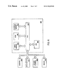
- FIG. 6 is a block diagram that illustrates an embodiment of the present invention.
- a semiconductor wafer is processed on a plurality of different processing tools, and a unique tool identifier is stored along with a set of process parameters for each tool, as by an MES.
- the wafer is inspected using an inspection tool, such as the WF7xx SeriesTM Wafer Inspection System available from Applied Materials of Santa Clara, Calif., and a list of the tool identifiers is generated from data retrieved from the MES, along with a defect map, and displayed at the inspection tool.
- the user may then request that the set of process parameters, including tool parameters (e.g., preventive maintenance conditioris), for any of the tools identified on the list be retrieved from the MES and displayed at the inspection tool.
- tool parameters e.g., preventive maintenance conditioris
- the user is automatically provided with a list of the tools visited by the wafer and has easy access to the process parameters used at each of those tools.
- This information along with the defect map (and other data gathered from defect review procedures, if performed), facilitates tracing the causes of defects to their source, such as to a particular process step or to a particular piece of processing equipment.
- the process of tracing the causes of defects to their source is further automated. Suspected defect sites are reviewed, identified and classified, either at the inspection tool or at a stand-alone review machine. Then the classes of defects are correlated with the parameters of particular tools on the list of tools visited by the wafer. An alarm is generated if a total number of defects in a specific one of the defect classes is about equal to or greater than a predetermined number for the specific defect class, and the tool identifier associated with the specific one of the defect classes is displayed at the inspection tool, thereby pointing out a faulty tool that is a probable cause of the defects.
- FIGS. 1-4 An embodiment of the present invention is illustrated in FIGS. 1-4.
- the present invention is implemented at an inspection tool 300 , as shown in FIG. 3, comprising an imager 310 for imaging the surface of a wafer at high speed, typically using a photo multiplier (PMT) or CCD and an illumination source such as a lamp or a laser.
- Inspection tool 300 further comprises a processor 320 , which preferably performs the analysis disclosed herein electronically, and a monitor 330 for displaying results of the analyses of processor 320 .
- Processor 320 is in communication with a conventional MES 340 , a conventional YMS 380 and, in one embodiment of the invention described below, a review station 350 .
- a semiconductor wafer W is processed to have a plurality of patterned integrated circuit dies 1000 .
- wafer W is initially subjected to a processing step at a processing tool at step 200 (FIG. 2 ), then a tool identifier unique to the processing tool is stored in MES 340 (FIG. 3) along with a set of process parameters used at the tool (see step 205 ).
- MES 340 FIG. 3
- it is determined (either manually by the user or automatically by MES 340 ) whether another processing step is to be performed on wafer W before it is to be inspected. If so, the wafer is brought to another processing tool, and steps 200 , 205 and 210 are repeated.
- wafer W is brought to inspection tool 300 and imaged by imager 310 (see step 215 ).
- a conventional defect map 400 is then produced at step 220 by processor 320 using statistical methods, typically involving algorithms and/or grey-scale analysis, to identify suspected locations 401 on wafer W having a high probability of having a defect.
- a list of tool identifiers associated with tools visited by wafer W is generated by processor 320 retrieving the tool identifier data stored in MES 340 (see step 235 ) and the list is displayed at inspection tool 300 at monitor 330 , along with defect map 400 (see step 240 ).
- the list of tool identifiers can be displayed on monitor 330 as a list of tool names, such as “Etcher 5” or “Cleaning Station 2”. Alternatively, the list may be displayed graphically, with icons representing different tool types.
- the list may be generated and displayed automatically after inspection (i.e., with no intervention by the user) or only when requested by the user.
- processor 320 determines a defect level for wafer W in a conventional manner, typically based on the number of suspected defect locations 401 and/or the density of suspected defect locations 401 , and compares the defect level with a predetermined defect level that represents the highest acceptable defect level. If the defect level is lower than the predetermined defect level, processing of wafer W continues at step 230 . However, if the defect level is about equal to or greater than the predetermined defect level, the list of tool identifiers associated with tools visited by wafer W is retrieved from MES 340 , and processing continues at step 235 .
- the user can select one or more of the tools on the list of tool identifiers, such as by moving a cursor to the appropriate tool name or icon, and obtain a display of the set of process parameters, which can include tool parameters, retrieved at step 245 from MES 340 by processor 320 and displayed on monitor 330 at step 250 .
- the user can more readily identify a probable cause of defects at the time the defects are discovered. Additionally, this information can be fed to YMS 380 for further statistical analysis off-line.
- defects are examined and classified, and the defect classes are correlated with the tools visited by wafer W.
- suspected defect locations 401 are reviewed to identify actual defects, each of the defects is examined and classified, and the defect classes are correlated with the tools visited by wafer W.
- a redetection procedure is carried out; e.g., after step 240 , at each suspected defect location 401 to determine the exact location of the defects.
- a conventional CCD imager such as imager 310 , or a conventional stand-alone SEM review station 350 (employing a processor 370 and a SEM 360 , such as SEMVisionTM available from Applied Materials of Santa Clara, Calif.), is used to image a pattern at a suspected defect location 401 and a reference pattern-at a corresponding location on an adjacent or other die on the same wafer which is not suspected of having a defect (see step 500 ).
- a suspected defect image is then compared to a corresponding reference pattern at step 505 by processor 320 (if the imaging is performed by imager 310 ) or by processor 370 (if the imaging is performed by SEM 360 ). If a difference is found between the suspected defective pattern and the reference pattern, the suspected defective pattern is determined to be a defect by processor 320 or processor 370 at step 510 .
- a more detailed review procedure is thereafter carried out on the individual defect sites, such as imaging with imager 310 or scanning with SEM 360 to produce a relatively high-resolution image, which is then analyzed at step 515 to determine the nature of the defect (e.g., a defective pattern, at particle, or a scratch) and to classify the defect accordingly.
- the analysis and classification of the defects can be carried out, as by one of processors 320 and 370 , using conventional pattern recognition techniques or using an automated technique as described in copending U.S. patent application Ser. No. 09/111,454, filed Jul. 8, 1998, entitled “Automatic Defect Classification With Invariant Core Classes”, the entire disclosure of which is hereby incorporated by reference.
- defects are classified, at step 500 a , while the wafer is being inspected and defect map 400 is being made (e.g., after step 220 ).
- This technique known as “On-The-Fly” Automatic Defect Classification, employs a modified version of inspection tool 300 ; for example, the WF-736 DUO wafer inspection tool available from Applied Materials of Santo Clara, Calif., whose operation is based on the fact that different defect types have different optical scattering signatures, which signatures are registered at strategically positioned multiple detectors (e.g., photo multipliers) as they scan the wafer.
- On-The-Fly Automatic Defect Classification is described in an article entitled “Enhanced Yield Potential Using ‘On-the-fly’ Automatic Defect Classification”, by Reinhold Ott and Andy Skumanich, [publication name, date and pages], the entire disclosure of which is herein incorporation by reference. Since this technique enables the acquisition of important defect information while the inspection is being performed, defect classification is carried out without a loss in production throughput.
- the tools on the list of tool identifiers are correlated to the defect classes by processor 320 , based upon the user's experiential knowledge of the causes of particular classes of defects. For example, if wafer W visited a chemical-mechanical polishing (CMP) machine, defects classified as scratches may be correlated with the particular CMP machine wafer W visited, based on the user's past observations that CMP machines commonly cause scratch defects.
- CMP chemical-mechanical polishing
- Processor 320 or processor 370 preferably counts the number of defects in each class of defects (see step 525 ). It is determined at step 530 , as by processor 320 or processor 370 , whether the number of defects in one of the classes exceeds a predetermined amount reflecting the maximum allowable number of defects in that particular class, referred to as a “class alarm level”. If the class alarm level is not reached, the next class is so analyzed (see step 535 ). If the number of defects in any one of the classes exceeds the predetermined class alarm level for that class, an alarm signal is generated, as by processor 320 , and monitor 320 displays the tool identifier associated with the specific defect class, thereby indicating to the user a possibly faulty tool.
- FIG. 6 is a block diagram that illustrates an embodiment of the invention shown in FIG. 3 .
- processor 320 includes a bus 602 or other communication mechanism for communicating information, and a central processing unit (CPU) 604 coupled with bus 602 for processing information.
- processor 320 also includes a main memory 606 , such as a random access memory (RAM) or other dynamic storage device, coupled to bus 602 for storing information and instructions to be executed by CPU 604 .
- Main memory 606 also may be used for storing temporary variables or other intermediate information during execution of instructions to be executed by CPU 604 .
- Processor 320 further includes a read only memory (ROM) 608 or other static storage device coupled to bus 602 for storing static information and instructions for CPU 604 .
- ROM read only memory
- a storage device 610 such as a magnetic disk or optical disk, is provided and coupled to bus 602 for storing information and instructions.
- Processor 320 is coupled, as via bus 602 , to monitor 330 (FIG. 3 ), such as a cathode ray tube (CRT), for displaying information to the user.
- monitor 330 such as a cathode ray tube (CRT)
- An input device 614 is coupled to bus 602 for communicating information and command selections to CPU 604 .
- cursor control 616 is Another type of user input device, such as a mouse, a trackball, or cursor direction keys for communicating direction information and command selections to CPU 604 and for controlling cursor movement on monitor 330 .
- Imager 310 (FIG. 3) inputs data representative of images of a semiconductor wafer under inspection, as discussed above, to bus 602 . Such data may be stored in main memory 606 and/or storage device 610 , and used by CPU 604 as it executes instructions. Imager 310 may also receive instructions via bus 602 from CPU 604 .
- the invention is related to the use of processor 320 for inspecting the surface of a semiconductor wafer.
- inspection of the surface of a semiconductor wafer is provided by processor 320 in response to CPU 604 executing one or more sequences of one or more instructions contained in main memory 606 .
- Such instructions may be read into main memory 606 from another computer-readable medium, such as storage device 610 .
- Execution of the sequences of instructions contained in main memory 606 causes CPU 604 to perform the process steps described above.
- processors in a multi-processing arrangement may also be employed to execute the sequences of instructions contained in main memory 606 .
- hard-wired circuitry may be used in place of or in combination with software instructions to implement the invention.
- embodiments of the invention are not limited to any specific combination of hardware circuitry and software.
- the programming of the apparatus is readily accomplished by one of ordinary skill in the art provided with the flow charts of FIG. 2 and FIG. 5 .
- Non-volatile media include, for example, optical or magnetic disks, such as storage device 610 .
- Volatile media include dynamic memory, such as main memory 606 .
- Transmission media include coaxial cable, copper wire and fiber optics, including the wires that comprise bus 602 . Transmission media can also take the form of acoustic or light waves, such as those generated during radio frequency (RF) and infrared (IR) data communications.
- RF radio frequency
- IR infrared
- Computer-readable media include, for example, a floppy disk, a flexible disk, hard disk, magnetic tape, any other magnetic medium, a CD-ROM, DVD, any other optical medium, punch cards, paper tape, any other physical medium with patterns of holes, a RAM, a PROM, and EPROM, a FLASH-EPROM, any other memory chip or cartridge, or any other medium from which a computer can read.
- Various forms of computer-readable media may be involved in carrying out one or more sequences of one or more instructions to CPU 604 for execution.
- the instructions may initially be borne on a magnetic disk of a remote computer.
- the remote computer can load the instructions into its dynamic memory and send the instructions over a telephone line using a modem.
- a modem local to processor 320 can receive the data on the telephone line and use an infrared transmitter to convert the data to an infrared signal.
- An infrared detector coupled to bus 602 can receive the data carried in the infrared signal and place the data on bus 602 .
- Bus 602 carries the data to main memory 606 , from which CPU 604 retrieves and executes the instructions.
- the instructions received by main memory 606 may optionally be stored on storage device 610 either before or after execution by CPU 604 .
- the inventive semiconductor wafer inspection technique provides real-time information identifying the tools visited by wafers under inspection and the process parameters including tool parameters used at those tools, thereby facilitating investigation of the causes of defects and enabling effective corrective action to be implemented at the time the defects are discovered.
- the present invention contributes to the maintenance of high production throughput.
- the inventive methodology enables early identification of a faulty tool.
- the present invention is applicable to the inspection of any semiconductor wafer, and is especially useful for in-process inspection of semiconductor wafers during manufacture of high density semiconductor devices with submicron design features.
Priority Applications (5)
| Application Number | Priority Date | Filing Date | Title |
|---|---|---|---|
| US09/358,512 US6763130B1 (en) | 1999-07-21 | 1999-07-21 | Real time defect source identification |
| JP2000213273A JP2001085491A (ja) | 1999-07-21 | 2000-07-13 | リアルタイム欠陥原因決定 |
| EP00306142A EP1071128A3 (fr) | 1999-07-21 | 2000-07-19 | Procédé d'identification en temps réel de sources de défauts sur des substrats semiconducteurs |
| TW089114479A TW484197B (en) | 1999-07-21 | 2000-07-19 | Real time defect source identification |
| KR1020000041976A KR100742425B1 (ko) | 1999-07-21 | 2000-07-21 | 반도체 웨이퍼 검사 방법 및 반도체 웨이퍼를 검사하는 명령들을 보유하는 컴퓨터-판독가능 매체 |
Applications Claiming Priority (1)
| Application Number | Priority Date | Filing Date | Title |
|---|---|---|---|
| US09/358,512 US6763130B1 (en) | 1999-07-21 | 1999-07-21 | Real time defect source identification |
Publications (1)
| Publication Number | Publication Date |
|---|---|
| US6763130B1 true US6763130B1 (en) | 2004-07-13 |
Family
ID=23409966
Family Applications (1)
| Application Number | Title | Priority Date | Filing Date |
|---|---|---|---|
| US09/358,512 Expired - Lifetime US6763130B1 (en) | 1999-07-21 | 1999-07-21 | Real time defect source identification |
Country Status (5)
| Country | Link |
|---|---|
| US (1) | US6763130B1 (fr) |
| EP (1) | EP1071128A3 (fr) |
| JP (1) | JP2001085491A (fr) |
| KR (1) | KR100742425B1 (fr) |
| TW (1) | TW484197B (fr) |
Cited By (34)
| Publication number | Priority date | Publication date | Assignee | Title |
|---|---|---|---|---|
| US20020054703A1 (en) * | 2000-11-09 | 2002-05-09 | Takashi Hiroi | Pattern inspection method and apparatus |
| US20030135295A1 (en) * | 2002-01-14 | 2003-07-17 | Applied Materials, Inc. | Defect source identifier with static manufacturing execution system |
| US6850811B1 (en) * | 2002-02-28 | 2005-02-01 | Advanced Micro Devices, Inc. | Analyzing error signals based on fault detection |
| US20050061242A1 (en) * | 2003-09-19 | 2005-03-24 | Dainippon Screen Mfg. Co., Ltd. | Substrate processing apparatus for performing photolithography |
| US20050075841A1 (en) * | 2003-08-05 | 2005-04-07 | Netanel Peles | Automated defect classification system and method |
| US20050075749A1 (en) * | 2003-10-03 | 2005-04-07 | Jung-Yi Tsai | Quality assurance system and method |
| US20050082476A1 (en) * | 1996-03-29 | 2005-04-21 | Takashi Hiroi | Electron beam inspection method and apparatus and semiconductor manufacturing method and its manufacturing line utilizing the same |
| US20050248756A1 (en) * | 2004-05-10 | 2005-11-10 | Long-Hui Lin | Method of defect inspection |
| US20050251276A1 (en) * | 2004-04-23 | 2005-11-10 | Taiwan Semiconductor Manufacturing Co., Ltd. | System and method for real-time fault detection, classification, and correction in a semiconductor manufacturing environment |
| US20060050950A1 (en) * | 2004-09-09 | 2006-03-09 | Hung-En Tai | Method of Managing Wafer Defects |
| US20060258023A1 (en) * | 2005-05-10 | 2006-11-16 | Lsi Logic Corporation | Method and system for improving integrated circuit manufacturing yield |
| US20060279729A1 (en) * | 2005-06-10 | 2006-12-14 | Vistec Semiconductor Systems Gmbh | Method of inspecting semiconductor wafers taking the SAW design into account |
| US20060293870A1 (en) * | 2005-06-10 | 2006-12-28 | Rassi Andrew T | Method and system for tracking quality events |
| US20070035322A1 (en) * | 2005-08-10 | 2007-02-15 | Joong-Wuk Kang | Testing method detecting localized failure on a semiconductor wafer |
| KR100733590B1 (ko) | 2003-09-08 | 2007-06-28 | 가부시끼가이샤 도시바 | 반도체장치의 제조시스템 및 반도체장치의 제조방법 |
| US20070171404A1 (en) * | 2006-01-26 | 2007-07-26 | Orbotech Ltd | System and method for inspecting patterned devices having microscopic conductors |
| US7263451B1 (en) * | 2004-10-25 | 2007-08-28 | Advanced Micro Devices, Inc. | Method and apparatus for correlating semiconductor process data with known prior process data |
| US20070219738A1 (en) * | 2006-03-15 | 2007-09-20 | Applied Materials, Inc. | Tool health information monitoring and tool performance analysis in semiconductor processing |
| CN100388451C (zh) * | 2004-11-02 | 2008-05-14 | 力晶半导体股份有限公司 | 缺陷检测方法 |
| US20090099675A1 (en) * | 2005-12-02 | 2009-04-16 | Alexander Staroselsky | System and Method for Optimizing Transmission Component Life and Transmission Power |
| US20100057239A1 (en) * | 2008-08-29 | 2010-03-04 | Keisuke Masuda | Semiconductor manufacturing apparatus |
| US20120050522A1 (en) * | 2010-08-24 | 2012-03-01 | Research In Motion Limited | Method of and apparatus for verifying assembly components of a mobile device |
| US20150022654A1 (en) * | 2013-07-22 | 2015-01-22 | Applied Materials Israel Ltd. | Closed-loop automatic defect inspection and classification |
| CN106531657A (zh) * | 2017-01-13 | 2017-03-22 | 京隆科技(苏州)有限公司 | 无墨点晶圆外观检查方法及其检查系统 |
| US9607233B2 (en) | 2012-04-20 | 2017-03-28 | Applied Materials Israel Ltd. | Classifier readiness and maintenance in automatic defect classification |
| US9665795B2 (en) | 2013-05-30 | 2017-05-30 | Samsung Sds Co., Ltd. | Method and apparatus for identifying root cause of defect using composite defect map |
| US9715723B2 (en) | 2012-04-19 | 2017-07-25 | Applied Materials Israel Ltd | Optimization of unknown defect rejection for automatic defect classification |
| US10043264B2 (en) | 2012-04-19 | 2018-08-07 | Applied Materials Israel Ltd. | Integration of automatic and manual defect classification |
| US20180364687A1 (en) * | 2017-06-19 | 2018-12-20 | Panasonic Intellectual Property Management Co., Ltd. | Mounting board manufacturing system |
| US20190293669A1 (en) * | 2018-03-22 | 2019-09-26 | Applied Materials Israel Ltd. | System, method and computer program product for classifying defects |
| CN110998463A (zh) * | 2017-01-18 | 2020-04-10 | Asml荷兰有限公司 | 用于缺陷检查的知识推荐 |
| CN113837983A (zh) * | 2020-06-08 | 2021-12-24 | 长鑫存储技术有限公司 | 一种晶圆缺陷分析方法、系统、设备和介质 |
| US11568198B2 (en) | 2018-09-12 | 2023-01-31 | Applied Materials, Inc. | Deep auto-encoder for equipment health monitoring and fault detection in semiconductor and display process equipment tools |
| US11663548B2 (en) | 2020-11-30 | 2023-05-30 | Toyota Motor Engineering & Manufacturing North America, Inc. | System and method for rapid defect entry |
Families Citing this family (24)
| Publication number | Priority date | Publication date | Assignee | Title |
|---|---|---|---|---|
| US6640151B1 (en) | 1999-12-22 | 2003-10-28 | Applied Materials, Inc. | Multi-tool control system, method and medium |
| US6708074B1 (en) | 2000-08-11 | 2004-03-16 | Applied Materials, Inc. | Generic interface builder |
| US6694284B1 (en) | 2000-09-20 | 2004-02-17 | Kla-Tencor Technologies Corp. | Methods and systems for determining at least four properties of a specimen |
| US6633831B2 (en) | 2000-09-20 | 2003-10-14 | Kla Tencor Technologies | Methods and systems for determining a critical dimension and a thin film characteristic of a specimen |
| US6891627B1 (en) | 2000-09-20 | 2005-05-10 | Kla-Tencor Technologies Corp. | Methods and systems for determining a critical dimension and overlay of a specimen |
| US6782337B2 (en) | 2000-09-20 | 2004-08-24 | Kla-Tencor Technologies Corp. | Methods and systems for determining a critical dimension an a presence of defects on a specimen |
| US6812045B1 (en) | 2000-09-20 | 2004-11-02 | Kla-Tencor, Inc. | Methods and systems for determining a characteristic of a specimen prior to, during, or subsequent to ion implantation |
| US6673637B2 (en) | 2000-09-20 | 2004-01-06 | Kla-Tencor Technologies | Methods and systems for determining a presence of macro defects and overlay of a specimen |
| US7188142B2 (en) | 2000-11-30 | 2007-03-06 | Applied Materials, Inc. | Dynamic subject information generation in message services of distributed object systems in a semiconductor assembly line facility |
| US7160739B2 (en) | 2001-06-19 | 2007-01-09 | Applied Materials, Inc. | Feedback control of a chemical mechanical polishing device providing manipulation of removal rate profiles |
| US7698012B2 (en) | 2001-06-19 | 2010-04-13 | Applied Materials, Inc. | Dynamic metrology schemes and sampling schemes for advanced process control in semiconductor processing |
| US20030199112A1 (en) | 2002-03-22 | 2003-10-23 | Applied Materials, Inc. | Copper wiring module control |
| KR20040040737A (ko) * | 2002-11-07 | 2004-05-13 | 삼성전자주식회사 | 반도체 웨이퍼 검사 방법 및 장치 |
| US7272459B2 (en) | 2002-11-15 | 2007-09-18 | Applied Materials, Inc. | Method, system and medium for controlling manufacture process having multivariate input parameters |
| US8359494B2 (en) * | 2002-12-18 | 2013-01-22 | Globalfoundries Inc. | Parallel fault detection |
| US6993404B2 (en) * | 2003-07-11 | 2006-01-31 | Mks Instruments, Inc. | Graphical user interface with process quality indicator |
| KR100546796B1 (ko) | 2003-07-21 | 2006-01-25 | 동부아남반도체 주식회사 | 두께와 광학 이미지의 라이브러리를 이용한 절연막검사방법 |
| KR100761851B1 (ko) | 2006-06-30 | 2007-09-28 | 삼성전자주식회사 | 실시간으로 최적화되는 반도체 소자의 전기적 검사를 위한 컴퓨터로 실행 가능한 저장매체 및 그 적용방법 |
| JP4952371B2 (ja) * | 2007-05-22 | 2012-06-13 | 凸版印刷株式会社 | カラーフィルタ生産における膜キズ自動発生防止方法及びその方法を用いた膜キズ自動発生防止システム |
| EP2447889A1 (fr) * | 2010-10-29 | 2012-05-02 | Siemens Aktiengesellschaft | Procédé pour la modélisation d'une gestion de défauts dans un procédé de fabrication et pour traiter le défaut pendant le procédé de fabrication basé sur ladite gestion de défauts |
| KR101535419B1 (ko) | 2013-05-31 | 2015-07-09 | 삼성에스디에스 주식회사 | 불량 셀 클러스터링 방법 및 그 장치 |
| JP6922694B2 (ja) * | 2017-11-27 | 2021-08-18 | オムロン株式会社 | 管理システム、管理装置、管理方法、及びプログラム |
| CN109698139A (zh) * | 2018-12-27 | 2019-04-30 | 上海华力微电子有限公司 | 晶圆缺陷光学照片实时采集系统及采集方法 |
| US11176656B2 (en) * | 2019-02-28 | 2021-11-16 | Fei Company | Artificial intelligence-enabled preparation end-pointing |
Citations (22)
| Publication number | Priority date | Publication date | Assignee | Title |
|---|---|---|---|---|
| US4519041A (en) * | 1982-05-03 | 1985-05-21 | Honeywell Inc. | Real time automated inspection |
| US4581762A (en) * | 1984-01-19 | 1986-04-08 | Itran Corporation | Vision inspection system |
| US5539752A (en) | 1995-06-30 | 1996-07-23 | Advanced Micro Devices, Inc. | Method and system for automated analysis of semiconductor defect data |
| DE19641414A1 (de) | 1995-10-09 | 1997-04-10 | Kti Semiconductor Ltd | Verfahren und Vorrichtung zur Einteilung eines Fehlers auf einem Halbleiterwafer |
| US5649169A (en) * | 1995-06-20 | 1997-07-15 | Advanced Micro Devices, Inc. | Method and system for declustering semiconductor defect data |
| US5777901A (en) * | 1995-09-29 | 1998-07-07 | Advanced Micro Devices, Inc. | Method and system for automated die yield prediction in semiconductor manufacturing |
| US5801965A (en) * | 1993-12-28 | 1998-09-01 | Hitachi, Ltd. | Method and system for manufacturing semiconductor devices, and method and system for inspecting semiconductor devices |
| US5814829A (en) * | 1995-07-11 | 1998-09-29 | Qc Optics, Inc. | Multistation surface inspection system |
| US5847821A (en) * | 1997-07-10 | 1998-12-08 | Advanced Micro Devices, Inc. | Use of fiducial marks for improved blank wafer defect review |
| EP0910123A1 (fr) | 1996-03-19 | 1999-04-21 | Hitachi, Ltd. | Systeme de commande de processus |
| US5910011A (en) * | 1997-05-12 | 1999-06-08 | Applied Materials, Inc. | Method and apparatus for monitoring processes using multiple parameters of a semiconductor wafer processing system |
| US5966459A (en) * | 1997-07-17 | 1999-10-12 | Advanced Micro Devices, Inc. | Automatic defect classification (ADC) reclassification engine |
| US5971586A (en) * | 1995-04-21 | 1999-10-26 | Sony Corporation | Identifying causes of semiconductor production yield loss |
| US5982921A (en) * | 1990-11-16 | 1999-11-09 | Applied Materials, Inc. | Optical inspection method and apparatus |
| US6049895A (en) * | 1996-12-09 | 2000-04-11 | Nec Corporation | Failure analyzer with distributed data processing network and method used therein |
| US6185511B1 (en) * | 1997-11-28 | 2001-02-06 | Advanced Micro Devices, Inc. | Method to accurately determine classification codes for defects during semiconductor manufacturing |
| US6259960B1 (en) * | 1996-11-01 | 2001-07-10 | Joel Ltd. | Part-inspecting system |
| US6360133B1 (en) * | 1999-06-17 | 2002-03-19 | Advanced Micro Devices, Inc. | Method and apparatus for automatic routing for reentrant process |
| US6373054B2 (en) * | 1996-03-29 | 2002-04-16 | Hitachi, Ltd. | Electron beam inspection method and apparatus and semiconductor manufacturing method and its manufacturing line utilizing the same |
| US6404911B2 (en) * | 1989-07-12 | 2002-06-11 | Hitachi, Ltd. | Semiconductor failure analysis system |
| US6408220B1 (en) * | 1999-06-01 | 2002-06-18 | Applied Materials, Inc. | Semiconductor processing techniques |
| US6427093B1 (en) * | 1999-10-07 | 2002-07-30 | Advanced Micro Devices, Inc. | Method and apparatus for optimal wafer-by-wafer processing |
Family Cites Families (5)
| Publication number | Priority date | Publication date | Assignee | Title |
|---|---|---|---|---|
| US5274434A (en) * | 1990-04-02 | 1993-12-28 | Hitachi, Ltd. | Method and apparatus for inspecting foreign particles on real time basis in semiconductor mass production line |
| KR19980021213A (ko) * | 1996-09-14 | 1998-06-25 | 김광호 | 반도체 웨이퍼 상의 결함 검사방법 |
| US5886896A (en) * | 1996-11-19 | 1999-03-23 | Advanced Micro Devices, Inc. | Method and apparatus for integrated control of a sensor in a manufacturing processing station |
| JPH10173021A (ja) * | 1996-12-12 | 1998-06-26 | Mitsubishi Electric Corp | 製造ライン解析方法及び製造ライン解析装置 |
| JP3324447B2 (ja) * | 1997-05-27 | 2002-09-17 | 松下電器産業株式会社 | 歩留阻害要因推定方法 |
-
1999
- 1999-07-21 US US09/358,512 patent/US6763130B1/en not_active Expired - Lifetime
-
2000
- 2000-07-13 JP JP2000213273A patent/JP2001085491A/ja active Pending
- 2000-07-19 TW TW089114479A patent/TW484197B/zh not_active IP Right Cessation
- 2000-07-19 EP EP00306142A patent/EP1071128A3/fr not_active Withdrawn
- 2000-07-21 KR KR1020000041976A patent/KR100742425B1/ko not_active IP Right Cessation
Patent Citations (22)
| Publication number | Priority date | Publication date | Assignee | Title |
|---|---|---|---|---|
| US4519041A (en) * | 1982-05-03 | 1985-05-21 | Honeywell Inc. | Real time automated inspection |
| US4581762A (en) * | 1984-01-19 | 1986-04-08 | Itran Corporation | Vision inspection system |
| US6404911B2 (en) * | 1989-07-12 | 2002-06-11 | Hitachi, Ltd. | Semiconductor failure analysis system |
| US5982921A (en) * | 1990-11-16 | 1999-11-09 | Applied Materials, Inc. | Optical inspection method and apparatus |
| US5801965A (en) * | 1993-12-28 | 1998-09-01 | Hitachi, Ltd. | Method and system for manufacturing semiconductor devices, and method and system for inspecting semiconductor devices |
| US5971586A (en) * | 1995-04-21 | 1999-10-26 | Sony Corporation | Identifying causes of semiconductor production yield loss |
| US5649169A (en) * | 1995-06-20 | 1997-07-15 | Advanced Micro Devices, Inc. | Method and system for declustering semiconductor defect data |
| US5539752A (en) | 1995-06-30 | 1996-07-23 | Advanced Micro Devices, Inc. | Method and system for automated analysis of semiconductor defect data |
| US5814829A (en) * | 1995-07-11 | 1998-09-29 | Qc Optics, Inc. | Multistation surface inspection system |
| US5777901A (en) * | 1995-09-29 | 1998-07-07 | Advanced Micro Devices, Inc. | Method and system for automated die yield prediction in semiconductor manufacturing |
| DE19641414A1 (de) | 1995-10-09 | 1997-04-10 | Kti Semiconductor Ltd | Verfahren und Vorrichtung zur Einteilung eines Fehlers auf einem Halbleiterwafer |
| EP0910123A1 (fr) | 1996-03-19 | 1999-04-21 | Hitachi, Ltd. | Systeme de commande de processus |
| US6373054B2 (en) * | 1996-03-29 | 2002-04-16 | Hitachi, Ltd. | Electron beam inspection method and apparatus and semiconductor manufacturing method and its manufacturing line utilizing the same |
| US6259960B1 (en) * | 1996-11-01 | 2001-07-10 | Joel Ltd. | Part-inspecting system |
| US6049895A (en) * | 1996-12-09 | 2000-04-11 | Nec Corporation | Failure analyzer with distributed data processing network and method used therein |
| US5910011A (en) * | 1997-05-12 | 1999-06-08 | Applied Materials, Inc. | Method and apparatus for monitoring processes using multiple parameters of a semiconductor wafer processing system |
| US5847821A (en) * | 1997-07-10 | 1998-12-08 | Advanced Micro Devices, Inc. | Use of fiducial marks for improved blank wafer defect review |
| US5966459A (en) * | 1997-07-17 | 1999-10-12 | Advanced Micro Devices, Inc. | Automatic defect classification (ADC) reclassification engine |
| US6185511B1 (en) * | 1997-11-28 | 2001-02-06 | Advanced Micro Devices, Inc. | Method to accurately determine classification codes for defects during semiconductor manufacturing |
| US6408220B1 (en) * | 1999-06-01 | 2002-06-18 | Applied Materials, Inc. | Semiconductor processing techniques |
| US6360133B1 (en) * | 1999-06-17 | 2002-03-19 | Advanced Micro Devices, Inc. | Method and apparatus for automatic routing for reentrant process |
| US6427093B1 (en) * | 1999-10-07 | 2002-07-30 | Advanced Micro Devices, Inc. | Method and apparatus for optimal wafer-by-wafer processing |
Non-Patent Citations (1)
| Title |
|---|
| Reinhold Ott, et al., "Yield Enhancement with Wafer Inspection Using On-the-fly Automatic Defect Classification," Micro, (Canon Communications, publisher; T. Cheyney, ed.), Jun. 1999, vol. 17, 6, p. 47-59. |
Cited By (64)
| Publication number | Priority date | Publication date | Assignee | Title |
|---|---|---|---|---|
| US20050082476A1 (en) * | 1996-03-29 | 2005-04-21 | Takashi Hiroi | Electron beam inspection method and apparatus and semiconductor manufacturing method and its manufacturing line utilizing the same |
| US7122796B2 (en) * | 1996-03-29 | 2006-10-17 | Hitachi Ltd. | Electron beam inspection method and apparatus and semiconductor manufacturing method and its manufacturing line utilizing the same |
| US7957579B2 (en) | 1998-11-30 | 2011-06-07 | Hitachi, Ltd. | Pattern inspection method and apparatus |
| US20100246933A9 (en) * | 1998-11-30 | 2010-09-30 | Takashi Hiroi | Pattern Inspection Method And Apparatus |
| US20080056559A1 (en) * | 1998-11-30 | 2008-03-06 | Takashi Hiroi | Pattern Inspection Method And Apparatus |
| US20070269101A1 (en) * | 2000-11-09 | 2007-11-22 | Takashi Hiroi | Pattern inspection method and apparatus |
| US7266235B2 (en) * | 2000-11-09 | 2007-09-04 | Hitachi, Ltd. | Pattern inspection method and apparatus |
| US7457453B2 (en) | 2000-11-09 | 2008-11-25 | Hitachi, Ltd. | Pattern inspection method and apparatus |
| US20020057831A1 (en) * | 2000-11-09 | 2002-05-16 | Takashi Hiroi | Pattern inspection method and apparatus |
| US20080063257A1 (en) * | 2000-11-09 | 2008-03-13 | Takashi Hiroi | Pattern Inspection Method And Apparatus |
| US7894658B2 (en) | 2000-11-09 | 2011-02-22 | Hitachi, Ltd. | Pattern inspection method and apparatus |
| US20020054703A1 (en) * | 2000-11-09 | 2002-05-09 | Takashi Hiroi | Pattern inspection method and apparatus |
| US7133550B2 (en) * | 2000-11-09 | 2006-11-07 | Hitachi, Ltd. | Pattern inspection method and apparatus |
| US20030135295A1 (en) * | 2002-01-14 | 2003-07-17 | Applied Materials, Inc. | Defect source identifier with static manufacturing execution system |
| US6850811B1 (en) * | 2002-02-28 | 2005-02-01 | Advanced Micro Devices, Inc. | Analyzing error signals based on fault detection |
| US20050075841A1 (en) * | 2003-08-05 | 2005-04-07 | Netanel Peles | Automated defect classification system and method |
| KR100733590B1 (ko) | 2003-09-08 | 2007-06-28 | 가부시끼가이샤 도시바 | 반도체장치의 제조시스템 및 반도체장치의 제조방법 |
| US20050061242A1 (en) * | 2003-09-19 | 2005-03-24 | Dainippon Screen Mfg. Co., Ltd. | Substrate processing apparatus for performing photolithography |
| US7525650B2 (en) * | 2003-09-19 | 2009-04-28 | Dainippon Screen Mfg., Co., Ltd. | Substrate processing apparatus for performing photolithography |
| US6957116B2 (en) * | 2003-10-03 | 2005-10-18 | Taiwan Semiconductor Manufcturing Co., Ltd. | Quality assurance system and method |
| US20050075749A1 (en) * | 2003-10-03 | 2005-04-07 | Jung-Yi Tsai | Quality assurance system and method |
| US6980873B2 (en) * | 2004-04-23 | 2005-12-27 | Taiwan Semiconductor Manufacturing Company, Ltd. | System and method for real-time fault detection, classification, and correction in a semiconductor manufacturing environment |
| US20050251276A1 (en) * | 2004-04-23 | 2005-11-10 | Taiwan Semiconductor Manufacturing Co., Ltd. | System and method for real-time fault detection, classification, and correction in a semiconductor manufacturing environment |
| US7382451B2 (en) * | 2004-05-10 | 2008-06-03 | Powerchip Semiconductor Corp. | Method of defect inspection |
| US20050248756A1 (en) * | 2004-05-10 | 2005-11-10 | Long-Hui Lin | Method of defect inspection |
| US20060050950A1 (en) * | 2004-09-09 | 2006-03-09 | Hung-En Tai | Method of Managing Wafer Defects |
| US7412090B2 (en) | 2004-09-09 | 2008-08-12 | Powerchip Semiconductor Corp. | Method of managing wafer defects |
| US7263451B1 (en) * | 2004-10-25 | 2007-08-28 | Advanced Micro Devices, Inc. | Method and apparatus for correlating semiconductor process data with known prior process data |
| CN100388451C (zh) * | 2004-11-02 | 2008-05-14 | 力晶半导体股份有限公司 | 缺陷检测方法 |
| US20060258023A1 (en) * | 2005-05-10 | 2006-11-16 | Lsi Logic Corporation | Method and system for improving integrated circuit manufacturing yield |
| US20060293870A1 (en) * | 2005-06-10 | 2006-12-28 | Rassi Andrew T | Method and system for tracking quality events |
| US20060279729A1 (en) * | 2005-06-10 | 2006-12-14 | Vistec Semiconductor Systems Gmbh | Method of inspecting semiconductor wafers taking the SAW design into account |
| US7514949B2 (en) | 2005-08-10 | 2009-04-07 | Samsung Electronics Co., Ltd. | Testing method detecting localized failure on a semiconductor wafer |
| US20070035322A1 (en) * | 2005-08-10 | 2007-02-15 | Joong-Wuk Kang | Testing method detecting localized failure on a semiconductor wafer |
| US7840301B2 (en) * | 2005-12-02 | 2010-11-23 | United Technologies Corporation | System and method for optimizing transmission component life and transmission power |
| US20090099675A1 (en) * | 2005-12-02 | 2009-04-16 | Alexander Staroselsky | System and Method for Optimizing Transmission Component Life and Transmission Power |
| US7391510B2 (en) * | 2006-01-26 | 2008-06-24 | Orbotech Ltd | System and method for inspecting patterned devices having microscopic conductors |
| US20070171404A1 (en) * | 2006-01-26 | 2007-07-26 | Orbotech Ltd | System and method for inspecting patterned devices having microscopic conductors |
| US7630858B1 (en) * | 2006-03-15 | 2009-12-08 | Applied Materials, Inc. | Tool health information monitoring and tool performance analysis in semiconductor processing |
| US20070219738A1 (en) * | 2006-03-15 | 2007-09-20 | Applied Materials, Inc. | Tool health information monitoring and tool performance analysis in semiconductor processing |
| US7454312B2 (en) | 2006-03-15 | 2008-11-18 | Applied Materials, Inc. | Tool health information monitoring and tool performance analysis in semiconductor processing |
| TWI382483B (zh) * | 2006-03-15 | 2013-01-11 | Applied Materials Inc | 在半導體製程中之工具健康資訊監控及工具效能分析 |
| US20100057239A1 (en) * | 2008-08-29 | 2010-03-04 | Keisuke Masuda | Semiconductor manufacturing apparatus |
| US20120050522A1 (en) * | 2010-08-24 | 2012-03-01 | Research In Motion Limited | Method of and apparatus for verifying assembly components of a mobile device |
| US10043264B2 (en) | 2012-04-19 | 2018-08-07 | Applied Materials Israel Ltd. | Integration of automatic and manual defect classification |
| US9715723B2 (en) | 2012-04-19 | 2017-07-25 | Applied Materials Israel Ltd | Optimization of unknown defect rejection for automatic defect classification |
| US9607233B2 (en) | 2012-04-20 | 2017-03-28 | Applied Materials Israel Ltd. | Classifier readiness and maintenance in automatic defect classification |
| US9665795B2 (en) | 2013-05-30 | 2017-05-30 | Samsung Sds Co., Ltd. | Method and apparatus for identifying root cause of defect using composite defect map |
| US20150022654A1 (en) * | 2013-07-22 | 2015-01-22 | Applied Materials Israel Ltd. | Closed-loop automatic defect inspection and classification |
| US10114368B2 (en) * | 2013-07-22 | 2018-10-30 | Applied Materials Israel Ltd. | Closed-loop automatic defect inspection and classification |
| US10901402B2 (en) | 2013-07-22 | 2021-01-26 | Applied Materials Israel, Ltd. | Closed-loop automatic defect inspection and classification |
| CN106531657A (zh) * | 2017-01-13 | 2017-03-22 | 京隆科技(苏州)有限公司 | 无墨点晶圆外观检查方法及其检查系统 |
| US11650576B2 (en) | 2017-01-18 | 2023-05-16 | Asml Netherlands B.V. | Knowledge recommendation for defect review |
| CN110998463B (zh) * | 2017-01-18 | 2023-08-25 | Asml荷兰有限公司 | 用于缺陷检查的知识推荐的服务器和方法 |
| CN110998463A (zh) * | 2017-01-18 | 2020-04-10 | Asml荷兰有限公司 | 用于缺陷检查的知识推荐 |
| US20180364687A1 (en) * | 2017-06-19 | 2018-12-20 | Panasonic Intellectual Property Management Co., Ltd. | Mounting board manufacturing system |
| US10824137B2 (en) * | 2017-06-19 | 2020-11-03 | Panasonic Intellectual Property Management Co., Ltd. | Mounting board manufacturing system |
| US10921334B2 (en) * | 2018-03-22 | 2021-02-16 | Applied Materials Israel Ltd. | System, method and computer program product for classifying defects |
| US20190293669A1 (en) * | 2018-03-22 | 2019-09-26 | Applied Materials Israel Ltd. | System, method and computer program product for classifying defects |
| US11568198B2 (en) | 2018-09-12 | 2023-01-31 | Applied Materials, Inc. | Deep auto-encoder for equipment health monitoring and fault detection in semiconductor and display process equipment tools |
| US11948061B2 (en) | 2018-09-12 | 2024-04-02 | Applied Materials, Inc. | Deep auto-encoder for equipment health monitoring and fault detection in semiconductor and display process equipment tools |
| CN113837983A (zh) * | 2020-06-08 | 2021-12-24 | 长鑫存储技术有限公司 | 一种晶圆缺陷分析方法、系统、设备和介质 |
| CN113837983B (zh) * | 2020-06-08 | 2023-09-15 | 长鑫存储技术有限公司 | 一种晶圆缺陷分析方法、系统、设备和介质 |
| US11663548B2 (en) | 2020-11-30 | 2023-05-30 | Toyota Motor Engineering & Manufacturing North America, Inc. | System and method for rapid defect entry |
Also Published As
| Publication number | Publication date |
|---|---|
| EP1071128A2 (fr) | 2001-01-24 |
| KR100742425B1 (ko) | 2007-07-24 |
| JP2001085491A (ja) | 2001-03-30 |
| EP1071128A3 (fr) | 2008-06-25 |
| KR20010029984A (ko) | 2001-04-16 |
| TW484197B (en) | 2002-04-21 |
Similar Documents
| Publication | Publication Date | Title |
|---|---|---|
| US6763130B1 (en) | Real time defect source identification | |
| US6466895B1 (en) | Defect reference system automatic pattern classification | |
| US6922482B1 (en) | Hybrid invariant adaptive automatic defect classification | |
| US6987873B1 (en) | Automatic defect classification with invariant core classes | |
| US6556955B2 (en) | Method of determining lethality of defects in circuit pattern inspection, method of selecting defects to be reviewed, and inspection system of circuit patterns involved with the methods | |
| US5982920A (en) | Automated defect spatial signature analysis for semiconductor manufacturing process | |
| US8799831B2 (en) | Inline defect analysis for sampling and SPC | |
| US7205555B2 (en) | Defect inspection apparatus and defect inspection method | |
| US7113628B1 (en) | Defect image classifying method and apparatus and a semiconductor device manufacturing process based on the method and apparatus | |
| US6496958B1 (en) | Yield prediction and statistical process control using predicted defect related yield loss | |
| US8189205B2 (en) | Surface inspection tool and surface inspection method | |
| US20080298670A1 (en) | Method and its apparatus for reviewing defects | |
| KR20080065584A (ko) | 검사 레시피의 확립을 위한 방법 및 시스템 | |
| JP2003007786A (ja) | 半導体基板の検査方法およびその装置 | |
| JP2003240731A (ja) | 欠陥検査方法及びその装置 | |
| US20110285839A1 (en) | Defect observation method and device using sem | |
| US6643006B1 (en) | Method and system for reviewing a semiconductor wafer using at least one defect sampling condition | |
| WO2021022100A1 (fr) | Procédé de surveillance de processus à l'aide d'inspections optiques | |
| Campbell et al. | In-Line Defectivity Methodology for a GaAs Manufacturing Facility |
Legal Events
| Date | Code | Title | Description |
|---|---|---|---|
| AS | Assignment |
Owner name: APPLIED MATERIALS, INC., CALIFORNIA Free format text: ASSIGNMENT OF ASSIGNORS INTEREST;ASSIGNOR:MAIMON, AMOTZ;REEL/FRAME:010100/0884 Effective date: 19990714 |
|
| AS | Assignment |
Owner name: APPLIED MATERIALS, INC., CALIFORNIA Free format text: ASSIGNMENT OF ASSIGNORS INTEREST;ASSIGNOR:SOMEKH, SASSON;REEL/FRAME:010125/0613 Effective date: 19990715 |
|
| STCF | Information on status: patent grant |
Free format text: PATENTED CASE |
|
| FPAY | Fee payment |
Year of fee payment: 4 |
|
| FPAY | Fee payment |
Year of fee payment: 8 |
|
| FPAY | Fee payment |
Year of fee payment: 12 |