US6714459B2 - Nonvolatile semiconductor memory device and method of detecting overerased cell - Google Patents
Nonvolatile semiconductor memory device and method of detecting overerased cell Download PDFInfo
- Publication number
- US6714459B2 US6714459B2 US10/241,752 US24175202A US6714459B2 US 6714459 B2 US6714459 B2 US 6714459B2 US 24175202 A US24175202 A US 24175202A US 6714459 B2 US6714459 B2 US 6714459B2
- Authority
- US
- United States
- Prior art keywords
- cell
- verify
- voltage
- overerased
- time
- Prior art date
- Legal status (The legal status is an assumption and is not a legal conclusion. Google has not performed a legal analysis and makes no representation as to the accuracy of the status listed.)
- Expired - Lifetime
Links
Images


Classifications
-
- G—PHYSICS
- G11—INFORMATION STORAGE
- G11C—STATIC STORES
- G11C16/00—Erasable programmable read-only memories
- G11C16/02—Erasable programmable read-only memories electrically programmable
- G11C16/06—Auxiliary circuits, e.g. for writing into memory
- G11C16/34—Determination of programming status, e.g. threshold voltage, overprogramming or underprogramming, retention
- G11C16/3404—Convergence or correction of memory cell threshold voltages; Repair or recovery of overerased or overprogrammed cells
- G11C16/3409—Circuits or methods to recover overerased nonvolatile memory cells detected during erase verification, usually by means of a "soft" programming step
-
- G—PHYSICS
- G11—INFORMATION STORAGE
- G11C—STATIC STORES
- G11C16/00—Erasable programmable read-only memories
- G11C16/02—Erasable programmable read-only memories electrically programmable
- G11C16/06—Auxiliary circuits, e.g. for writing into memory
- G11C16/34—Determination of programming status, e.g. threshold voltage, overprogramming or underprogramming, retention
- G11C16/3404—Convergence or correction of memory cell threshold voltages; Repair or recovery of overerased or overprogrammed cells
-
- G—PHYSICS
- G11—INFORMATION STORAGE
- G11C—STATIC STORES
- G11C16/00—Erasable programmable read-only memories
- G11C16/02—Erasable programmable read-only memories electrically programmable
- G11C16/06—Auxiliary circuits, e.g. for writing into memory
- G11C16/26—Sensing or reading circuits; Data output circuits
- G11C16/28—Sensing or reading circuits; Data output circuits using differential sensing or reference cells, e.g. dummy cells
Definitions
- the present invention relates to a nonvolatile semiconductor memory device enabling high-speed erase where a low threshold is used as an erased state, and to a method of detecting an overerased cell in the nonvolatile semiconductor memory device.
- FIG. 12 is a schematic cross sectional view showing this ETOX-type flash memory cell.
- a floating gate 5 is formed on a source 1 , a drain 2 and a substrate (well) 3 between the source and the drain via a tunnel oxide film 4 .
- a control gate 7 is formed on the floating gate 5 via an interlayer insulating film 6 .
- a voltage Vpp for example, 10 V
- a reference voltage Vss for example, 0 V
- a voltage of 6 V is applied to the drain 2 . Consequently, a large amount of current is allowed to flow in a channel layer, hot electrons are generated in a portion on the drain 2 side where an electric field is high, and electrons are implanted into the floating gate 5 .
- a threshold voltage rises, and data is written to the memory cell.
- FIG. 13 shows threshold voltage distributions in a written state and an erased state. As shown in FIG. 13, the threshold voltage of a written memory cell is 5 V or higher. It is noted that open of the drain 2 in Table 1 means a voltage applied to the drain 2 of a memory cell to which data is not to be written.
- a voltage Vnn (for example, ⁇ 9 V) is applied to the control gate 7
- a voltage Vpe (for example, 6 V) is applied to the source 1
- the drain 2 is made open to pull electrons from the floating gate 5 to the source 1 side and lower the threshold voltage.
- the threshold voltage of an erased memory cell becomes 1.5-3 V as shown in FIG. 13 .
- a voltage of 1 V is applied to the drain 2 and a voltage of 5 V is applied to the control gate 7 . Then, when the memory cell is in an erased state, that is, when the threshold voltage is low, a current is allowed to flow into the cell and its state is determined as “1”. On the other hand, when the threshold voltage is high and the memory cell is in a written state, a current is not allowed to flow into the cell and its state is determined as “0”.
- write, erase and read operations are performed.
- processing is performed in units of relatively large blocks of 64 kB for example.
- some memory cells in a block where the erase processing is performed have a threshold voltage in a program state (high voltage) and others have a threshold voltage in an erased state (low voltage). That is, memory cells having two kinds of threshold voltages shown in FIG. 13 are mixed.
- the threshold voltages of the memory cells already in an erased state become in an excessively erased (overerased) state.
- the threshold voltages of the memory cells whose threshold voltages decreases more rapidly than others become in an overerased state. This is particularly problematic when the overerased state progresses, resulting in a negative threshold voltage.
- 0 V is applied to control gates of unselected memory cells at the time of read, write-verify or erase-verify.
- a memory cell having a negative threshold voltage exists among the unselected memory cells, a cell current is allowed to flow into this memory cell although the memory cell is not selected. Therefore, when a selected memory cell M 00 and an overerased cell M (1023, 0) are connected to the same bit line BL 0 as shown in FIG. 14, a cell current flowing into the unselected overerased cell M (1023, 0) is added to the cell current flowing into the selected memory cell M 00 .
- the cell current measured in the bit line BL 0 has a large value. Therefore, the threshold voltage of a program cell is apparently determined as low (an erased state).
- an operation cannot be performed precisely at the time of the read, write-verify or erase-verify, and, as a result, a normal device operation cannot be performed.
- FIG. 3 shows the fundamental algorithm.
- step S 1 when an erase operation is started, first, a program before erase is performed for all memory cells in step S 1 .
- the voltage applied at this time is the same as that of the write operation described above.
- step S 2 verify of the program before erase is performed. Detail description thereof is not given here, however, as a result of the verify of the program before erase, if there exists even one memory cell whose threshold voltage does not reach a predetermined voltage (5.0 V or higher in FIG. 13) because the program state is insufficient, the program is performed for the memory cell again, and the program and the verify are repeated until the threshold voltage of the memory cell becomes the predetermined voltage (5.0 V) or higher. Then, when the threshold voltage of the memory cell becomes the predetermined voltage (5.0 V) or higher, the program proceeds to the address of the next memory cell. Thus, when threshold voltages of all memory cells become the predetermined voltage or higher, the verify of the program before erase is terminated.
- step S 3 an erase pulse is applied.
- This erase pulse application processing is performed in a unit of blocks. That is, data is erased in all memory cells in a block at the same time by making the drain 2 open to apply ⁇ 9 V to the control gate 7 and 6 V to the source 1.
- step S 4 when the erase pulse application is terminated as described above, erase-verify is performed to determine whether all memory cells in the block have a predetermined threshold voltage or lower (3 V or lower in this case). Detail description is not given here, but, when a memory cell whose threshold voltage is not the predetermined voltage or lower is found, erase-verify is once stopped, and an erase pulse is applied again. This operation is repeated until threshold voltages of all memory cells become the predetermined voltage or lower.
- step S 5 overerased cell detection and a soft program described in detail later are performed. Then, the erase operation is terminated.
- FIG. 15 shows a general algorithm of the overerased cell detection performed in step S 5 in the flow chart of the erase operation shown in FIG. 3 .
- the flash memory cell array is configured by memory cells M arranged in a matrix, word lines WL connected to control gates of the memory cells M arranged in the line direction, bit lines BL connected to drains of the memory cells M arranged in the column direction and a common source line SL for connecting sources of all the memory cells M 00 to M (1023, 511) constituting a block.
- a threshold voltage Vt of a memory cell M (RA, CA) is verified, the memory cell M (RA, CA) being positioned at an intersection of the row address RA and the column address CA.
- step S 14 as a result of this verification, it is judged whether the threshold voltage Vt of the memory cell M (RA, CA) is higher than 0.5 V.
- step S 15 when the threshold voltage is higher than 0.5 V, it is determined that the memory cell M (RA, CA) is not in an overerased state, and processing proceeds to step S 15 .
- the threshold voltage when the threshold voltage is 0.5 V or lower, it is determined that the memory cell M (RA, CA) is in an overerased state (verify is performed), and processing proceeds to step S 19 .
- step S 15 the row address RA is incremented. As a result, when word line WL 0 is selected in step S 12 , word line WL 1 is selected.
- step S 18 the column address CA is incremented. As a result, when bit line BL 0 is selected in the aforementioned step S 11 , bit line BL 1 is selected. Then, processing returns to the aforementioned step S 12 , and the row address RA is returned to the initial value “0”. Then, when bit line BL 1 is selected in the aforementioned step S 18 , the threshold voltage Vt of a memory cell M 01 positioned at the intersection of word line WL 0 and bit line BL 1 is verified.
- step S 19 an initial value “0” is set in the number N of times a software program is performed.
- step S 20 a row address RA when an overerased state is determined in the step S 14 is stored in a register Xadd. Subsequently, software program processing is started.
- the reason why the row address RA of an overerased memory cell is stored in register Xadd is as follows.
- a memory cell M (RA, CA) When it is determined that a memory cell M (RA, CA) is in an overerased state, there are first and second cases.
- the threshold voltage of the memory cell M (RA, CA) lowers too rapidly depending on the variation of an erase characteristic.
- a cell current flows even into an unselected state and hence the threshold voltage of the memory cell M (RA, CA) is apparently detected as low because there exists a memory cell M having a negative threshold voltage among other memory cells M (RA+1, CA) to M ( 1023 , CA) which share a bit line BL with the memory cell M (RA, CA).
- a software program needs to be successively repeated for memory cells M (RA, CA) to M (1023, CA) connected to the same bit line BL a predetermined number of times until their threshold voltages become 0.5 or higher.
- the row address RA of the memory cell M (RA, CA) is stored in register Xadd.
- step S 21 a write pulse (program pulse) is applied to a memory cell M (RA, CA) to execute a software program for raising a threshold voltage Vt.
- step S 22 the threshold voltage Vt of the memory cell M (RA, CA) is verified.
- step S 23 as a result of the above verification, it is judged whether the threshold voltage Vt of the memory cell M (RA, CA) is higher than 0.5 V. As a result, when the threshold voltage is higher than 0.5 V, it is determined that the memory cell M (RA, CA) is not in an overerased state, and processing returns to the aforementioned step S 15 to continue the overerased cell detection processing. On the other hand, when the threshold voltage is 0.5 V or lower, processing proceeds to step S 24 .
- step S 24 since the threshold voltage Vt is still 0.5 V or lower even though the software program is executed for the memory cell M (RA, CA), the row address RA is incremented.
- step S 25 it is judged whether the row address RA is the final address RA MAX or higher. As a result, when the row address is the final address RA MAX or higher, processing proceeds to step S 26 , and when the row address is lower than the final address RA MAX , processing returns to the aforementioned step S 21 and software program processing is performed for the next memory cell M (RA, CA).
- step S 26 XADD, which is the content stored in register Xadd, is set in the row address RA.
- step S 27 the number N of times the software program is executed is incremented.
- step S 28 it is judged whether the number N of times the software program is executed is “10” or more. As a result, when N is less than “10”, processing returns to the aforementioned step S 21 and shifts to the next software program processing. On the other hand, when N is “10” or more, the erase operation is terminated as an erase failure.
- the software program processing is repeated up to 10 times for memory cells M 00 to M (1023, 0) until their threshold voltages Vt become higher than 0.5 V.
- a memory cell for reference (reference cell) Mr which has the same characteristic as that of main cells M and is used for verifying threshold voltages Vt of these main cells M. Furthermore, the threshold voltage Vt of a selected main cell M in the memory cell array is determined by comparing a cell current Ir flowing into this reference cell Mr and a cell current Im flowing into the selected main cell M.
- the threshold voltage Vt of the reference cell Mr is set as, for example, 3.0 V in advance. Consequently, an I-V characteristic of this reference cell Mr is as shown in FIG. 17, which indicates that, when 4.5 V is applied to word line WLref connected to the control gate of the reference cell Mr, the cell current Ir flows into the reference cell Mr.
- the cell current Im becomes higher than the cell current Ir (Im>Ir). This is judged by a sense amplifier as shown in FIG. 18 to verify whether the cell is an overerased state.
- the main cells M in the memory cell array are selected one by one and connected to the sense amplifier. Thereafter, 4.5 V is applied to the word line WLref of the reference cell Mr, while 2 V is applied to the word line WLmain of the selected main cell M. Thereby, it is successively verified whether the cell is in an overerased state.
- the conventional verify method for detecting a memory cell M in an overerased state has the following problems.
- the main cells M are verified one by one.
- 8 main cells M whose control gates are connected to one word line are verified in parallel. Since verify time of one block is expressed by (verify time of 1 memory cell M) ⁇ (number of memory cells in a block)/(number of cells processed in parallel), when 500 ns is required to verify one memory cell M, the verify time of one block in this case is
- this verify time is time required for a normal detection routine performed in steps S 11 to S 18 in FIG. 15 . Therefore, when a memory cell M in an overerased state is detected and consequently a software program is executed, a software program time and verify time which the software program involves are further added to the verify time of 33 ms.
- erase-verify and erase pulse application are alternately repeated in erase-verify performed in the step S 4 as shown in FIG. 3 so that threshold voltages of all memory cells M in a block become a predetermined voltage (3.0 V in FIG. 13) or lower. Furthermore, a variation in the erase characteristic of each memory cell M is not so actually wide as arises a problem. Therefore, in a normal condition, a memory cell in an overerased state rarely appears.
- the overerase detection time needs to be shortened because it is supposed that high-speed erase whose erase time is, for example, 10 ms or less is required.
- An object of the present invention is to provide a nonvolatile semiconductor memory device with which time of overerased cell detection essential for guarantee of reliability can be largely shortened in consideration to the present situation where an overerased cell rarely appears in a normal state.
- An object of the present invention is to provide a method of detecting such an overerased cell as the above.
- a first aspect of the present invention provides a nonvolatile semiconductor memory device comprising:
- a memory cell array including:
- a threshold voltage of each of the floating gate electric field effect transistors in a written state is higher than a threshold voltage of each of the floating gate electric field effect transistors in an erased state
- a erase processing means which performs erase processing where, by controlling voltages applied to the row lines, the column lines and the common wiring,
- fifthly first verify is performed to detect an overerased cell
- second verify is performed to specify the overerased cell by applying a voltage different from the voltage applied in the first verify to the row line
- the erase processing means when erase processing is performed by the erase processing means, verify is performed after erase pulse application and then a first verify for detecting an overerased cell is performed.
- a second verify for specifying the overerased cell is performed.
- a voltage different from the voltage applied to a row line at the time of the first verify is applied to the row line. Therefore, by lowering the voltage applied to the row line at the time of the first verify to the level of the threshold voltage in a floating gate electric field effect transistor to be an overerased cell, the first verify of a plurality of floating gate electric field effect transistors can be performed in a batch with low currents.
- detection sensitivity is increased and hence specific speed of the overerased cell can be increased.
- the erase processing means has the first verify means which performs the first verify in units of the column lines by applying a voltage to all row lines connected to control gates of the plurality of floating gate electric field effect transistors whose drains are commonly connected to the column line so that one floating gate electric field effect transistor in an overerased state at most exists among the plurality of floating gate electric field effect transistors, and that a leakage current when the floating gate electric field effect transistor in an overerased state is unselected in a normal operation can be equal to a predetermined value or lower.
- the overerased cell detection time is shortened.
- the voltage applied to the row line is set so that there exists one floating gate electric field effect transistor in an overerased state at most, and that a leakage current when this floating gate electric field effect transistor in an overerased state is unselected is equal to a predetermined value or lower in a normal operation, and therefore, lower power consumption can be achieved.
- a second aspect of the present invention provides a method of detecting an overerased cell in the nonvolatile semiconductor memory device according to the firs aspect of the invention, wherein
- pass or failure is determined at time of the first verify and the second verify by comparing a current value of the column line connected to a drain of a reference cell and a current value of the column line connected to a drain of a target cell composed of a floating gate electric field effect transistor to be verified, the reference cell being composed of a floating gate electric field effect transistor which has the same structure as that of the aforementioned floating gate electric field effect transistor and is not written or erased.
- the first verify and the second verify are performed by current sense using the reference cell. Therefore, a current value flowing into a target cell constituted by the floating gate electric field effect transistor to be verified can be directly detected. Therefore, for example, the first verify for a plurality of target cells whose drains are commonly connected to the column line can be performed in a batch.
- the first verify and the second verify are performed by using the same reference cell.
- the number of the reference cells is reduced to half, and expansion of the chip area is prevented. Furthermore, since current sense characteristics become the same at the time of the first verify and the second verify, there are less errors in detection of an overerased cell.
- a first voltage is lower than a second voltage
- a third voltage is lower than a fourth voltage
- the first voltage is lower than the third voltage
- a voltage applied to a row line connected to a control gate of the target cell at time of the first verify is defined as the first voltage
- a voltage applied to a row line connected to a control gate of the reference cell at time of first verify is defined as the second voltage
- a voltage applied to the row line connected to the control gate of the target cell at time of the second verify is defined as the third voltage
- a voltage applied to the row line connected to the control gate of the reference cell at time of the second verify is defined as the fourth voltage.
- the voltage applied to the row line on the reference cell side is higher than the voltage applied to the row line on the target cell side. Therefore, the state of the reference cell becomes stable, and detection accuracy is improved. Furthermore, the voltage applied to the row line on the target cell side at the time of the second verify is higher than the voltage applied to the row line on the target cell side at the time of the first verify. Therefore, sense sensitivity at the time of the second verify becomes higher than that of the first verify.
- current values in the reference cell and the target cell are compared by a sense amplifier, and at time of the first verify, a predetermined voltage for detecting an overerased cell is applied to all the row lines in the block, while the column lines are successively selected and connected to the sense amplifier to detect the overerased cell in units of the column lines.
- the first verify is performed in units of the column lines. Therefore, the number of times of verify is reduced in comparison with the case that the first verify is performed in units of individual floating gate electric field effect transistors, and hence the overerased cell detection time is shortened.
- a voltage different from the voltage applied to the row lines at time of the first verify is successively applied to the row lines, and only a column line determined as including an overerased cell at time of the first verify is connected to the sense amplifier so as to specify the overerased cell in units of individual target cells.
- the overerased cell is specified in units of individual target cells for a column line for which presence of an overerased cell is determined at the time of the first verify. Therefore, the overerased cell is precisely specified.
- the floating gate electric field effect transistor having a threshold voltage between 0 and 1 V inclusive in the memory cell array is detected as the overerased cell at time of the first verify and the second verify.
- a floating gate electric field effect transistor having a threshold voltage between 0 V and 1 V inclusive is detected as the overerased cell. Therefore, the maximum value of a leakage current in a normal operation when detection omission occurs is restricted to the leakage current of a floating gate electric field effect transistor having a threshold voltage of 0 V. Furthermore, a small number of overerased cells positioned in the vicinity of the lower limit in distribution of threshold voltages of all the floating gate electric field effect transistors belonging to the memory cell array can be detected.
- a third aspect of the invention provides a method of detecting an overerased cell in the nonvolatile semiconductor memory device according to the first aspect of the invention, wherein
- pass or failure at time of the first verify is determined based on a voltage value of the column line connected to the drain of a target cell composed of a floating gate electric field effect transistor to be verified, and
- the pass or failure at time of the second verify is determined by comparing a current value of the column line connected to the drain of a reference cell and a current value of the column line connected to the drain of the target cell, the reference cell being composed of a floating gate electric field effect transistor which has the same structure as that of the aforementioned floating gate electric field effect transistor and is not written or erased.
- the first verify is performed by voltage sense. Therefore, an overerased cell can be detected with favorable sensitivity in a short time.
- a voltage between 0 and 1 V inclusive is applied to the row line connected to the control gate of the target cell at time of first verify.
- a floating gate electric field effect transistor having a threshold voltage of between 0 V and 1 V inclusive is detected as the overerased cell. Therefore, the maximum value of a leakage current in a normal operation when detection omission occurs is restricted to the leakage current of a floating gate electric field effect transistor having a threshold voltage of 0 V. Furthermore, a small number of overerased cells positioned in the vicinity of the lower limit in distribution of threshold voltages of all the floating gate electric field effect transistors belonging to the memory cell array can be detected.
- a voltage of a column line connected to the target cell is detected by a sense amplifier at time of the first verify, and a leakage current to be detected is controlled by controlling time when the column line connected to the drain of the target cell is connected to the sense amplifier.
- a sixth voltage is lower than a seventh voltage
- a voltage applied to a row line connected to the control gate of the target cell at time of the first verify is defined as a fifth voltage
- a voltage applied to the row line connected to the control gate of the target cell at time of second verify is defined as the sixth voltage
- a voltage applied to a row line connected to the control gate of the reference cell at time of the second verify is defined as the seventh voltage.
- the voltage applied to the row line on the reference cell side at the time of the second verify is higher than the voltage applied to the row line on the target cell side. Therefore, the state of the reference cell becomes stable, and detection precision is improved.
- a voltage value of the column line connected to the target cell is detected by a first sense amplifier, and at time of the first verify, a predetermined voltage for detecting an overerased cell is applied to all the row lines in the block, and the column lines are successively selected to be connected to the first sense amplifier so as to detect the overerased cell in units of the column lines.
- the first verify is performed in units of the column lines. Therefore, the number of times of verify is reduced in comparison with the case that the first verify is performed in units of individual floating gate electric field effect transistors, and therefore, the overerased cell detection time is shortened.
- current values in the reference cell and the target cell are compared by a second sense amplifier at time of the second verify, and
- a voltage different from the voltage applied to the row line at time of the first verify is successively applied at time of the second verify, and only column lines determined as including an overerased cell at time of the first verify are successively connected to the second sense amplifier so as to specify the overerased cells in units of individual target cells.
- the overerased cell is specified in units of individual target cells for a column line in which presence of an overerased cell is determined at the time of the first verify. Therefore, the overerased cell is precisely specified.
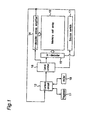
- FIG. 1 is a schematic block diagram showing a nonvolatile semiconductor memory device according to the present invention
- FIG. 2 shows a specific configuration of a memory cell array in FIG. 1;
- FIG. 3 is a flow chart of an erase operation
- FIG. 4 shows distribution of threshold voltages Vt of all memory cells at a termination point of erase-verify in the erase operation shown in FIG. 3;
- FIG. 5 is a flow chart of an overerased cell detecting operation
- FIG. 6 shows an I-V characteristic of a main cell
- FIG. 7 shows an I-V characteristic of a reference cell
- FIG. 8 shows an I-V characteristic of an overerased cell having a threshold voltage Vt of 0 V
- FIG. 9 is a circuit diagram of a sense amplifier for performing current detection by current sense
- FIG. 10 is a circuit diagram of a sense amplifier for performing current detection by voltage sense
- FIG. 11 shows operation timing of the sense amplifier shown in FIG. 10
- FIG. 12 is a schematic cross sectional view showing an ETOX-type flash memory cell
- FIG. 13 shows threshold voltage distributions in a written state and an erased state
- FIG. 14 is a view for explaining the reason why a precise verify operation cannot be performed due to presence of an overerased cell
- FIG. 15 is a flow chart of a conventional overerased cell detecting operation
- FIG. 16 shows an I-V characteristic of a main cell at the time of conventional overerased cell detection
- FIG. 17 shows an I-V characteristic of a reference cell at the time of conventional overerased cell detection
- FIG. 18 is a circuit diagram of a sense amplifier for performing current detection by current sense at the time of overerased cell detection.
- FIG. 1 is a block diagram showing a configuration of a nonvolatile semiconductor memory device according to a first embodiment of the present invention.
- a register 11 stores a row address when a software program is performed in an erase operation as described later.
- Reference numeral 13 denotes a memory cell array.
- Reference numeral 14 denotes a source driver on which a Y decoder and a sense amplifier are mounted.
- the Y decoder includes a drive circuit for receiving a control signal from a control circuit 12 so as to apply a voltage to each bit line.
- the sense amplifier is connected to each bit line.
- Reference numeral 15 denotes a gate driver on which an X decoder is mounted.
- the X decoder includes a drive circuit for receiving a control signal from the control circuit 12 so as to apply a voltage to each word line.
- Reference numeral 16 denotes a level shifter. The level shifter level-converts the control signal from the control circuit 12 to a voltage for write, erase or read and thereafter outputs the voltage.
- Reference numeral 17 denotes a source switch is for selecting a common source line.
- Reference numeral 18 denotes a ROM (Read Only Memory) in which programs for write processing, erase processing and read processing and so forth by the control circuit 12 are stored.
- FIG. 2 shows a configuration of the memory cell array 13 in the nonvolatile semiconductor memory device shown in FIG. 1 .
- the configuration of the memory cell array 13 is a flash memory having the same configuration as that of the conventional memory cell array.
- FIG. 3 is a flow chart showing an algorithm for an erase operation by an erase processing program stored in the ROM 18 .
- This erase operation is performed in the order of a before-erase program, verify of the before-erase program, erase pulse application, erase-verify and overerased cell detection.
- the verify of the before-erase program, erase pulse application and erase-verify are performed in the same manner as in the case of the above-described conventional erase operation.
- the algorithm about the overerased cell detection processing is different from the conventional one.
- an erase processing means in a first aspect of the invention is configured by steps S 1 to S 5 in the erase operation shown in FIG. 3 using the control circuit 12 , level shifter 16 , source driver 14 , gate driver 15 and source switch 17 .
- step S 4 in the erase operation shown in FIG. 3 erase-verify and erase pulse application are alternately repeated so that threshold voltages Vt of all memory cells in a block to be erased are made equal to a predetermined voltage (3.0 V in FIG. 13) or lower.
- FIG. 4 shows a distribution state of the threshold voltages Vt of all memory cells in the block at this point.
- the horizontal axis represents the threshold voltage Vt (V) of a memory cell, and the vertical axis represents appearance probability (%) of the memory cell.
- FIG. 4 shows that 99.99% of threshold voltages Vt of all memory cells are 1.0 V or higher, and the appearance probability of a memory cell having a threshold voltage Vt of 0.5 V or less is about 0.005% at most.
- FIG. 6 shows an I-V characteristic of a main memory M in the block. As shown in FIG.
- FIG. 5 is a flow chart of an overerased cell detecting operation performed in step S 5 in the flow chart of the erase operation shown in FIG. 3 .
- an overerased cell detecting operation of this embodiment will be explained with reference to the flow chart shown in FIG. 5 and the configuration of the memory cell array shown in FIG. 2 .
- step S 32 threshold voltages Vt of memory cells M (0, CA) to M (1023, CA) positioned at this column address CA are verified in a batch.
- step S 33 as a result of this verification, it is judged whether the threshold voltages Vt of the memory cells M (0, CA) to M (1023, CA) are higher than 0.5 V. As a result, when the threshold voltages are higher than 0.5 V, it is determined that the memory cells M (0, CA) to M (1023, CA) are not in an overerased state, and processing proceeds to step S 34 . On the other hand, when the threshold voltages are 0.5 V or lower, it is determined that there is an overerased cell among the memory cells M (0, CA) to M (1023, CA), and proceeding proceeds to step S 36 .
- overerase-verify is performed for each bit line BL.
- cell currents flowing into 1024 memory cells from memory cells M 00 to M (1023, 0) are detected by bit line BL 0 .
- the threshold voltage Vt of a reference cell Mr is set as 3.0 V in advance, the reference cell Mr being provided separately from cells to which data is written or read.
- the cell current Ir is about 1 ⁇ A when the threshold voltage Vt of 3 V is applied to the gate electrode.
- the voltage applied to word lines WL 0 to WL 1023 corresponding to the main cells M (0, CA) to M (1023, CA) is thus reduced from the conventional 2 V (see FIG. 18) to 0.5 V so that a cell current Im is set to be small (about 1 ⁇ A).
- This reduction of voltage results from consideration of appearance probability of a memory cell M having a threshold voltage Vt of 1.0 V or lower as shown in FIG. 4 .
- appearance probability of a main cell M is 0.005% or less.
- This probability means existence of one or no cell among 1024 main cells M connected to one bit line BL.
- step S 35 the column address CA is incremented. Then, processing returns to the aforementioned step S 32 , and threshold voltages Vt of all main cells M connected to the next bit line BL are verified.
- a voltage of 0.5 V is applied to all word lines WL 0 to WL 1023 in the block and 3.0 V is also applied to word line WLref of the reference cell Mr as they are.
- cell currents currents of 1024 main cells M
- Ir cell current
- BL 2 , BL 3 , . . . , BL 511 while the column address CA is incremented.
- overerase-verify is terminated, and the erase processing operation is terminated.
- the first verify means in a second aspect of the invention is constituted by steps S 31 to S 35 in the overerased cell detecting operation shown in FIG. 5 .
- a leakage current when the memory cell M is unselected (0 V is applied to a word line) at the time of write-verify, erase-verify or read in a normal operation is suppressed to 1 ⁇ A or lower. That is, a device having a very low leakage current can also be selected.
- overerase-verify method of this embodiment since a low current of about 1 ⁇ A is detected for each bit line BL to judge the relationship of the current values, a current needs to be stabilized or sense sensitivity needs to be increased. Therefore, one overerase-verify time is 1 ⁇ s, which is longer than that (500 ns) of the conventional case where judgment is performed for each memory cell M. However, since verify in this embodiment is performed in a batch in units of bit lines BL, the total overerase-verify time becomes
- the verify time of this embodiment is largely shortened in comparison with the verify time of 3.3 ms in the conventional case where overerase-verify is performed in units of memory cells M. That is to say, time of a normal detection routine (steps S 31 to S 35 ) in an overerased cell detection is largely shortened in this embodiment.
- step S 36 When it is determined that the threshold voltage Vt is 0.5 V or lower in the step S 33 as described above, it is determined that an overerased cell exists among memory cells M (0, CA) to M (1023, CA), so that proceeding proceeds to step S 36 .
- step S 36 an initial value “0” is set in a row address RA.
- step S 37 the threshold voltage Vt of a memory cell M (RA, CA) is verified.
- step S 38 as a result of this verification, it is judged whether the threshold voltage Vt of the memory cell M (RA, CA) is higher than 0.5 V.
- step S 39 when the threshold voltage is higher than 0.5 V, it is determined that the memory cell M (RA, CA) is not in an overerased state, and processing proceeds to step S 39 .
- the threshold voltage is 0.5 V or lower, it is determined that the memory cell M (RA, CA) is in an overerased state, and proceeding proceeds to step S 41 .
- step S 39 the row address RA is incremented.
- step S 41 an initial value “0” is set in the number N of times a software program is executed.
- step S 42 the row address RA when the overerased state is determined in the aforementioned step S 38 is stored in the register (XADD) 11 .
- step S 43 the software program is executed for the memory cell M (RA, CA).
- a gate voltage Vg and a drain voltage are 5 V and 6 V, respectively.
- step S 44 the threshold voltage Vt of the memory cell M (RA, CA) is verified.
- step S 45 as a result of the verification, it is judged whether the threshold voltage Vt of the memory cell M (RA, CA) is higher than 0.5 V.
- the threshold voltage Vt of the memory cell M (RA, CA) is increased by the software program, and it is determined that the cell is not in an overerased state any longer. Then, processing returns to the aforementioned step S 34 , and overerased cell detection processing is continued. On the other hand, when the threshold voltage is 0.5 V or lower, processing proceeds to step S 46 .
- step S 46 the row address RA is incremented.
- step S 48 When the row address is lower than the final address RA MAX , processing returns to the aforementioned step S 43 and software program processing is performed for the next memory cell M (RA, CA).
- the software program processing is performed for the memory cell M (RA, CA) until its threshold voltage Vt becomes higher than 0.5 V.
- step S 48 XADD, which is the content stored in the register 11 , is set in the row address RA.
- step S 49 the number N of times the software program is executed is incremented.
- step S 50 it is judged whether the number N of times the software program is executed is “10” or more. When N is less than “10”, processing returns to the aforementioned step S 43 , and the next software program processing is performed. On the other hand, when N is “10” or more, erase failure is determined, and the erase operation is terminated.
- erase failure is stored in the register, and finally it is separately judged whether this small block in units of bits is replaced with another small block in units of bits, the device itself is not used, or the like.
- step S 37 , S 38 , S 44 and S 45 during the software program processing executed in steps S 36 to S 50 in this case, 4.5 V is applied to word line WLref of a reference cell Mr whose threshold voltage Vt is set as 3.0 V, 2.0 V is applied to word line WLmain of a selected main cell M, and 0 V is applied to word line WL of an unselected memory cell M. That is, in verify during the software program processing, the same voltages as those in verify in the conventional overerased cell detection processing shown in FIG. 18 are used. I-V characteristics of the main cell M and the reference cell Mr in this case are shown in FIGS. 16 and 17, respectively.
- a detection current value is thus increased in verify during the software program processing is as follows. That is, since a low current (1 ⁇ A) is used for detection in verify (steps S 32 and S 33 ) during the overerased cell detection processing performed in steps S 31 to S 35 , the current value is raised to increase sense sensitivity during the software program processing. Furthermore, even when threshold voltages Vt of individual main cells M whose drains are connected to the same bit line BL are higher than 0.5 V and cell currents Im are lower than 1 ⁇ A, a cell current flowing into each main cell M is added and 1 ⁇ A or higher is assumed, the threshold voltage Vt of main cells M whose drains are connected to the bit line BL as a whole may be determined as 0.5 V or lower. Therefore, this case needs to be separately considered. In this case, an increase of a current value also means that sense time in a verify routine during this software program processing is shortened.
- verify is performed in a batch in units of bit lines BL at the time of overerase-verify in an erase operation.
- a cell current of the reference cell Mr and a voltage applied to word line WL of a main cell M are set so as to have a detection level at which there can be one or no memory cell M having a threshold voltage equal to a predetermined threshold voltage Vt (for example, 0.5 V) or lower (overerased state) in one overerase-verify and a leakage current of an unselected memory cell M can be equal to a predetermined current value (for example, 1 ⁇ A) or lower in a normal operation.
- high-speed erase can be achieved by largely reducing the number of times verify is performed at the time of overerase-verify to shorten overerase-verify time. Furthermore, the cell current can be reduced to achieve low power consumption.
- re-detection is performed for each word line WL as in the case of the conventional device so that an overerased state is specified and this specified memory cell is recovered. At this time, a judgment current is raised to increase sense sensitivity so that speed to reach stable measurement is increased.
- overerase-verify is performed by voltage sense in the same memory cell array configuration in a nonvolatile semiconductor memory device as in the case of the first embodiment.
- the algorithm of an erase operation in this embodiment is executed according to the flow chart shown in FIG. 3 in the same way as that of the erase operation in the first embodiment and. Furthermore, the algorithm of an overerased cell detecting operation in this embodiment is executed according to the flow chart shown in FIG. 5 in the same way as that of the overerased cell detecting operation in the first embodiment.
- overerase-verify in an overerased cell detecting operation is the same as that in the first embodiment as follows. Specifically, verify is performed in a batch in units of bit lines. A voltage applied to a word line WL of a main cell M is also set so as to have a detection level at which there can be one or no memory cell M in an overerased state having a threshold voltage equal to a predetermined threshold voltage Vt (for example, 0.5 V) or lower in one overerase-verify.
- Vt for example, 0.5 V
- a leakage current of an unselected memory cell M can be a predetermined current value (for example, 1 ⁇ A) or lower in a normal operation as in the case of the overerase-verify in the first embodiment.
- the threshold voltage Vt of the reference cell Mr as shown in FIG. 18 is set as 3.0 V, and a voltage of 4.5 V is applied to word line WLref. Meanwhile, a voltage of 2.0 V is applied to a word line WLmain of a selected main cell M, while a voltage of 0 V is applied to a word line WL of an unselected memory cell M.
- this embodiment is different from the first embodiment in that current detection is performed by voltage sense as shown in FIG. 10 at the time of the overerase-verify (that is, the normal detection routine (steps S 31 to S 35 ) of the overerased cell detecting operation shown in FIG. 5 ).
- a set sense current value (however, there is no reference cell Mr) is 1 ⁇ A, and 0.5 V is applied to word lines WLmain of all the main cells M in a block in a batch.
- the operation timing of the voltage sense in this case is shown in FIG. 11 .
- the sense amplifier is constituted by a latching circuit 21 configured by connecting an input of one of two inverters using a power source voltage and a ground voltage as a power source to an output of the other and connecting an output of the one inverter to an input of the other, an nMOS transistor 22 connected to one output line (node A) of this latching circuit 21 and the power source and an nMOS transistor 23 connected to the node A and bit lines BL of main cells M (1024 memory cells M in units of bit lines BL). Furthermore, a control signal pre is inputted to a gate of the nMOS transistor 22 , and a control signal set is inputted to a gate of the nMOS transistor 23 .
- the sense amplifier having the above configuration performs the following operation to detect a current Im flowing into the main cell M. That is, as shown in FIG. 11, first, a level of the control signal set is set as “H” to turn on the nMOS transistor 23 . Consequently, the latching circuit 21 , which is a sense system, and a bit line BL of a main cell M to be judged are connected. Subsequently, the level of the control signal pre is set as “H” to turn on the nMOS transistor 22 . Then, a current is supplied from the power source via the nMOS transistor 22 to raise a voltage of the node A (precharge). Meanwhile, since the node A rises, the level of the node A is latched as “H” and the level of the node B is latched as “L” in the latching circuit 21 .
- the nMOS transistor 22 is turned off, while 0.5 V is applied to all the word lines WL 0 to WL 1023 of the main cells M to be judged (1024 memory cells M whose drains are connected to the bit line BL to be judged) in a batch. Then, when a main cell M having a threshold voltage Vt of 0.5 V or lower is included in the main cells M connected to the bit line BL, the cell current Im flows and hence the voltage of the node A lowers.
- the latch voltage of the latching circuit 21 is inverted, and the voltage level of the node A is latched as “L (ground potential)”, while the voltage level of the node B is latched as “H (power source voltage)”.
- the latching circuit 21 in this case is rapidly inverted when the voltage of the node A becomes lower than the inversion voltage, speed is high, and sense sensitivity is also high. Furthermore, when the voltage of the node A is inverted, it is determined that a memory cell in an overerased state is included (or, this may be a result of summing up of cell currents of all memory cells), a memory cell in an overerased state is specified and a software program is performed for this specified memory cell for each of the word lines. At the time of verify in this case, as described above, the reference cell Mr of the sense amplifier shown in FIG.
- a sense amplifier configured by a latching circuit 21 , an nMOS transistor 22 for precharging the node A (one output line) of this latching circuit 21 and an nMOS transistor 23 for connecting the node A and a bit line BL of a main cell M. Furthermore, in a normal detection routine of the above overerased cell detection processing, the node A and the bit line BL of the main cell M are connected, and then the level of the control signal pre is set as “H” and the node A is precharged for predetermined time. Then, 0.5 V is applied to word lines WL 0 to WL 1023 of all main cells M in a batch.
- verify time is shortened in comparison with the aforementioned conventional overerase-verify method.
- a voltage of 0.5 V is applied to a word line WLmain connected to a main cell M as shown in FIGS. 9 and 10, but the applied voltage is not limited to this voltage so long as it is 0-1 V.
- a maximum value of a leakage current in a normal operation when detection omission occurs can be restricted to a leakage current of an overerased cell having a threshold voltage of 0 V.
- one or none of overerased cells positioned in the vicinity of the lower limit in the threshold voltage distribution shown in FIG. 4 can be detected in one overerased cell detection.
Landscapes
- Read Only Memory (AREA)
Applications Claiming Priority (2)
| Application Number | Priority Date | Filing Date | Title |
|---|---|---|---|
| JP2001-276884 | 2001-09-12 | ||
| JP2001276884A JP3984445B2 (ja) | 2001-09-12 | 2001-09-12 | 不揮発性半導体メモリ装置のオーバーイレースセル検出方法 |
Publications (2)
| Publication Number | Publication Date |
|---|---|
| US20030067818A1 US20030067818A1 (en) | 2003-04-10 |
| US6714459B2 true US6714459B2 (en) | 2004-03-30 |
Family
ID=19101518
Family Applications (1)
| Application Number | Title | Priority Date | Filing Date |
|---|---|---|---|
| US10/241,752 Expired - Lifetime US6714459B2 (en) | 2001-09-12 | 2002-09-12 | Nonvolatile semiconductor memory device and method of detecting overerased cell |
Country Status (2)
| Country | Link |
|---|---|
| US (1) | US6714459B2 (ja) |
| JP (1) | JP3984445B2 (ja) |
Cited By (10)
| Publication number | Priority date | Publication date | Assignee | Title |
|---|---|---|---|---|
| US20040141378A1 (en) * | 1999-03-18 | 2004-07-22 | Kabushiki Kaisha Toshiba | Nonvolatile semiconductor memory |
| US20050078522A1 (en) * | 2003-10-08 | 2005-04-14 | Micron Technology, Inc. | Memory block erasing in a flash memory device |
| US20050216652A1 (en) * | 2004-03-25 | 2005-09-29 | Elite Semiconductor Memory Technology Inc. | Circuit and method for preventing nonvolatile memory from over-erase |
| US20060140011A1 (en) * | 2004-12-23 | 2006-06-29 | Yupin Fong | Reducing floating gate to floating gate coupling effect |
| US20070236998A1 (en) * | 2005-04-12 | 2007-10-11 | Yasuhiko Honda | Nonvolatile semiconductor memory device which stores multivalue data |
| US20080198660A1 (en) * | 2007-02-20 | 2008-08-21 | Nima Mokhlesi | Multiple pass write sequence for non-volatile storage |
| US20090154252A1 (en) * | 2007-12-13 | 2009-06-18 | Noboru Shibata | Semiconductor memory device capable of shortening erase time |
| US20100296331A1 (en) * | 2008-03-21 | 2010-11-25 | Micron Technology, Inc. | Sensing resistance variable memory |
| US20110164449A1 (en) * | 2007-07-26 | 2011-07-07 | Micron Technology, Inc. | Programming based on controller performance requirements |
| US20120140559A1 (en) * | 2009-08-19 | 2012-06-07 | Yingda Dong | Selective memory cell program and erase |
Families Citing this family (8)
| Publication number | Priority date | Publication date | Assignee | Title |
|---|---|---|---|---|
| US7038945B2 (en) * | 2004-05-07 | 2006-05-02 | Micron Technology, Inc. | Flash memory device with improved programming performance |
| US7583658B1 (en) * | 2004-06-17 | 2009-09-01 | Cisco Technology, Inc. | Signal processing allocation using credit prediction |
| US7272050B2 (en) * | 2004-08-10 | 2007-09-18 | Samsung Electronics Co., Ltd. | Non-volatile memory device and erase method of the same |
| JP4433400B2 (ja) * | 2004-12-09 | 2010-03-17 | レノボ シンガポール プライヴェート リミテッド | 無線ネットワーク通信用カード、該カードを組み込んだ装置、無線ネットワーク通信をサポートする装置、及び無線ネットワーク通信のために無線アクセスポイントを検出する方法 |
| JP5072446B2 (ja) * | 2007-06-15 | 2012-11-14 | スパンション エルエルシー | 半導体装置及びその制御方法 |
| US10062440B1 (en) * | 2017-06-20 | 2018-08-28 | Winbond Electronics Corp. | Non-volatile semiconductor memory device and reading method thereof |
| CN109872759B (zh) * | 2017-12-01 | 2023-07-25 | 兆易创新科技集团股份有限公司 | 一种存储器擦除方法及装置 |
| CN114758689A (zh) * | 2022-04-08 | 2022-07-15 | 珠海博雅科技股份有限公司 | 用于非易失性存储器的擦除方法和上电修复方法 |
Citations (7)
| Publication number | Priority date | Publication date | Assignee | Title |
|---|---|---|---|---|
| US5237535A (en) * | 1991-10-09 | 1993-08-17 | Intel Corporation | Method of repairing overerased cells in a flash memory |
| US5598368A (en) * | 1994-05-19 | 1997-01-28 | Hitachi, Ltd. | Batch erasable nonvolatile memory device and erasing method |
| US5642311A (en) * | 1995-10-24 | 1997-06-24 | Advanced Micro Devices | Overerase correction for flash memory which limits overerase and prevents erase verify errors |
| US6122198A (en) * | 1999-08-13 | 2000-09-19 | Advanced Micro Devices, Inc. | Bit by bit APDE verify for flash memory applications |
| US6442074B1 (en) * | 2001-02-28 | 2002-08-27 | Advanced Micro Devices, Inc. | Tailored erase method using higher program VT and higher negative gate erase |
| US6483752B2 (en) * | 2000-07-05 | 2002-11-19 | Sharp Kabushiki Kaisha | Erase method for nonvolatile semiconductor memory device |
| US6532175B1 (en) * | 2002-01-16 | 2003-03-11 | Advanced Micro Devices, In. | Method and apparatus for soft program verification in a memory device |
-
2001
- 2001-09-12 JP JP2001276884A patent/JP3984445B2/ja not_active Expired - Fee Related
-
2002
- 2002-09-12 US US10/241,752 patent/US6714459B2/en not_active Expired - Lifetime
Patent Citations (8)
| Publication number | Priority date | Publication date | Assignee | Title |
|---|---|---|---|---|
| US5237535A (en) * | 1991-10-09 | 1993-08-17 | Intel Corporation | Method of repairing overerased cells in a flash memory |
| JPH06290596A (ja) | 1991-10-09 | 1994-10-18 | Intel Corp | フラッシュメモリにおける過消去セルの修復方法 |
| US5598368A (en) * | 1994-05-19 | 1997-01-28 | Hitachi, Ltd. | Batch erasable nonvolatile memory device and erasing method |
| US5642311A (en) * | 1995-10-24 | 1997-06-24 | Advanced Micro Devices | Overerase correction for flash memory which limits overerase and prevents erase verify errors |
| US6122198A (en) * | 1999-08-13 | 2000-09-19 | Advanced Micro Devices, Inc. | Bit by bit APDE verify for flash memory applications |
| US6483752B2 (en) * | 2000-07-05 | 2002-11-19 | Sharp Kabushiki Kaisha | Erase method for nonvolatile semiconductor memory device |
| US6442074B1 (en) * | 2001-02-28 | 2002-08-27 | Advanced Micro Devices, Inc. | Tailored erase method using higher program VT and higher negative gate erase |
| US6532175B1 (en) * | 2002-01-16 | 2003-03-11 | Advanced Micro Devices, In. | Method and apparatus for soft program verification in a memory device |
Cited By (39)
| Publication number | Priority date | Publication date | Assignee | Title |
|---|---|---|---|---|
| US6856548B2 (en) * | 1999-03-18 | 2005-02-15 | Kabushiki Kaisha Toshiba | Nonvolatile semiconductor memory |
| US20040141378A1 (en) * | 1999-03-18 | 2004-07-22 | Kabushiki Kaisha Toshiba | Nonvolatile semiconductor memory |
| US20050078522A1 (en) * | 2003-10-08 | 2005-04-14 | Micron Technology, Inc. | Memory block erasing in a flash memory device |
| US6975538B2 (en) * | 2003-10-08 | 2005-12-13 | Micron Technology, Inc. | Memory block erasing in a flash memory device |
| US20050276119A1 (en) * | 2003-10-08 | 2005-12-15 | Micron Technology, Inc. | Memory block erasing in a flash memory device |
| US7180781B2 (en) | 2003-10-08 | 2007-02-20 | Micron Technology, Inc. | Memory block erasing in a flash memory device |
| US7305513B2 (en) * | 2004-03-25 | 2007-12-04 | Elite Semiconductor Memory Technology, Inc. | Circuit for preventing nonvolatile memory from over-erase |
| US20050216652A1 (en) * | 2004-03-25 | 2005-09-29 | Elite Semiconductor Memory Technology Inc. | Circuit and method for preventing nonvolatile memory from over-erase |
| US20060140011A1 (en) * | 2004-12-23 | 2006-06-29 | Yupin Fong | Reducing floating gate to floating gate coupling effect |
| US20070195602A1 (en) * | 2004-12-23 | 2007-08-23 | Yupin Fong | Reducing floating gate to floating gate coupling effect |
| US7230851B2 (en) | 2004-12-23 | 2007-06-12 | Sandisk Corporation | Reducing floating gate to floating gate coupling effect |
| US7397698B2 (en) | 2004-12-23 | 2008-07-08 | Sandisk Corporation | Reducing floating gate to floating gate coupling effect |
| US20070236998A1 (en) * | 2005-04-12 | 2007-10-11 | Yasuhiko Honda | Nonvolatile semiconductor memory device which stores multivalue data |
| US7414892B2 (en) * | 2005-04-12 | 2008-08-19 | Kabushiki Kaisha Toshiba | Nonvolatile semiconductor memory device which stores multivalue data |
| US20080198661A1 (en) * | 2007-02-20 | 2008-08-21 | Nima Mokhlesi | Non-volatile storage apparatus with variable initial program voltage magnitude |
| US20080198662A1 (en) * | 2007-02-20 | 2008-08-21 | Nima Mokhlesi | Dynamic verify based on threshold voltage distribution |
| US20080198665A1 (en) * | 2007-02-20 | 2008-08-21 | Nima Mokhlesi | Variable initial program voltage magnitude for non-volatile storage |
| US20080198664A1 (en) * | 2007-02-20 | 2008-08-21 | Nima Mokhlesi | Non-volatile storage apparatus with multiple pass write sequence |
| US20080198660A1 (en) * | 2007-02-20 | 2008-08-21 | Nima Mokhlesi | Multiple pass write sequence for non-volatile storage |
| US8395945B2 (en) | 2007-02-20 | 2013-03-12 | Sandisk Technologies Inc. | Variable initial program voltage magnitude for non-volatile storage |
| US7564711B2 (en) | 2007-02-20 | 2009-07-21 | Sandisk Corporation | Multiple pass write sequence for non-volatile storage |
| US7564715B2 (en) | 2007-02-20 | 2009-07-21 | Sandisk Corporation | Variable initial program voltage magnitude for non-volatile storage |
| US20090244977A1 (en) * | 2007-02-20 | 2009-10-01 | Nima Mokhlesi | Variable initial program voltage magnitude for non-volatile storage |
| US7616500B2 (en) | 2007-02-20 | 2009-11-10 | Sandisk Corporation | Non-volatile storage apparatus with multiple pass write sequence |
| US7616495B2 (en) | 2007-02-20 | 2009-11-10 | Sandisk Corporation | Non-volatile storage apparatus with variable initial program voltage magnitude |
| US7619930B2 (en) | 2007-02-20 | 2009-11-17 | Sandisk Corporation | Dynamic verify based on threshold voltage distribution |
| US8125832B2 (en) | 2007-02-20 | 2012-02-28 | Sandisk Technologies Inc. | Variable initial program voltage magnitude for non-volatile storage |
| US20110164449A1 (en) * | 2007-07-26 | 2011-07-07 | Micron Technology, Inc. | Programming based on controller performance requirements |
| US8611149B2 (en) * | 2007-07-26 | 2013-12-17 | Micron Technology | Programming based on controller performance requirements |
| US20140104944A1 (en) * | 2007-07-26 | 2014-04-17 | Micron Technology, Inc. | Programming based on controller performance requirements |
| US8953374B2 (en) * | 2007-07-26 | 2015-02-10 | Mircon Technology, Inc. | Programming based on controller performance requirements |
| US7995392B2 (en) | 2007-12-13 | 2011-08-09 | Kabushiki Kaisha Toshiba | Semiconductor memory device capable of shortening erase time |
| US20090154252A1 (en) * | 2007-12-13 | 2009-06-18 | Noboru Shibata | Semiconductor memory device capable of shortening erase time |
| US20100296331A1 (en) * | 2008-03-21 | 2010-11-25 | Micron Technology, Inc. | Sensing resistance variable memory |
| US8587984B2 (en) * | 2008-03-21 | 2013-11-19 | Micron Technology, Inc. | Sensing resistance variable memory |
| US8649207B2 (en) | 2008-03-21 | 2014-02-11 | Micron Technology, Inc. | Sensing resistance variable memory |
| US20120140559A1 (en) * | 2009-08-19 | 2012-06-07 | Yingda Dong | Selective memory cell program and erase |
| US8315093B2 (en) * | 2009-08-19 | 2012-11-20 | Sandisk Technologies Inc. | Selective memory cell program and erase |
| USRE45754E1 (en) | 2009-08-19 | 2015-10-13 | Sandisk Technologies Inc. | Selective memory cell program and erase |
Also Published As
| Publication number | Publication date |
|---|---|
| JP2003085985A (ja) | 2003-03-20 |
| US20030067818A1 (en) | 2003-04-10 |
| JP3984445B2 (ja) | 2007-10-03 |
Similar Documents
| Publication | Publication Date | Title |
|---|---|---|
| US6714459B2 (en) | Nonvolatile semiconductor memory device and method of detecting overerased cell | |
| JP3238574B2 (ja) | 不揮発性半導体記憶装置とその消去方法 | |
| US6330192B1 (en) | Nonvolatile semiconductor memory device and method of erasing data of nonvolatile semiconductor memory device | |
| US6122198A (en) | Bit by bit APDE verify for flash memory applications | |
| US6097638A (en) | Semiconductor memory device | |
| US7362616B2 (en) | NAND flash memory with erase verify based on shorter evaluation time | |
| US6515908B2 (en) | Nonvolatile semiconductor memory device having reduced erase time and method of erasing data of the same | |
| KR100280023B1 (ko) | 백 그라운드 오퍼레이션 모드를 갖는 불휘발성 반도체 기억 장치 | |
| US20080137436A1 (en) | Programming method for non-volatile memory and non-volatile memory-based programmable logic device | |
| US6229734B1 (en) | Nonvolatile semiconductor storage device having controlled cell threshold voltage distribution | |
| KR20010020770A (ko) | Nand형 불휘발성 메모리 | |
| US7376016B2 (en) | Method of writing to non-volatile semiconductor memory device storing information depending on variation in level of threshold voltage | |
| KR20010070320A (ko) | 불 휘발성 반도체 기억장치 | |
| JP2000123585A (ja) | 積層ゲ―トメモリデバイスのフロ―ティングゲ―トに電荷をチャ―ジする方法 | |
| US6947325B2 (en) | Non-volatile semiconductor memory device and controlling method of the same | |
| JP2001067882A (ja) | 不揮発性半導体記憶装置およびその消去方法 | |
| JPH0668688A (ja) | 不揮発性半導体装置 | |
| JP2689939B2 (ja) | 不揮発性半導体記憶装置 | |
| KR100924377B1 (ko) | 높은 칼럼 누설이 존재하는 nor 플래쉬 메모리 셀들을위한 정확한 검증 장치 및 방법 | |
| US7227784B2 (en) | Nonvolatile semiconductor memory device performing erase operation that creates narrow threshold distribution | |
| KR20030019854A (ko) | 메모리 셀 트랜지스터의 임계값 편차의 영향을 억제할 수있는 비휘발성 반도체 기억 장치 | |
| JP2735498B2 (ja) | 不揮発性メモリ | |
| JP2008130182A (ja) | 不揮発性半導体記憶装置 | |
| JPH11167800A (ja) | 半導体記憶装置 | |
| JPH09115292A (ja) | 半導体不揮発性記憶装置 |
Legal Events
| Date | Code | Title | Description |
|---|---|---|---|
| AS | Assignment |
Owner name: SHARP KABUSHIKI KAISHA, JAPAN Free format text: ASSIGNMENT OF ASSIGNORS INTEREST;ASSIGNOR:HIRANO, YASUAKI;REEL/FRAME:013551/0155 Effective date: 20021022 |
|
| STCF | Information on status: patent grant |
Free format text: PATENTED CASE |
|
| FEPP | Fee payment procedure |
Free format text: PAYOR NUMBER ASSIGNED (ORIGINAL EVENT CODE: ASPN); ENTITY STATUS OF PATENT OWNER: LARGE ENTITY |
|
| FPAY | Fee payment |
Year of fee payment: 4 |
|
| FPAY | Fee payment |
Year of fee payment: 8 |
|
| AS | Assignment |
Owner name: INTELLECTUAL PROPERTIES I KFT., HUNGARY Free format text: ASSIGNMENT OF ASSIGNORS INTEREST;ASSIGNOR:SHARP KABUSHIKI KAISHA;REEL/FRAME:027387/0650 Effective date: 20111115 |
|
| AS | Assignment |
Owner name: SAMSUNG ELECTRONICS CO., LTD, KOREA, REPUBLIC OF Free format text: ASSIGNMENT OF ASSIGNORS INTEREST;ASSIGNOR:INTELLECTUAL PROPERTIES I KFT.;REEL/FRAME:035120/0878 Effective date: 20141222 |
|
| AS | Assignment |
Owner name: SAMSUNG ELECTRONICS CO., LTD., KOREA, REPUBLIC OF Free format text: CORRECTIVE ASSIGNMENT TO CORRECT THE ASSIGNEE NAME PREVIOUSLY RECORDED AT REEL: 035120 FRAME: 0878. ASSIGNOR(S) HEREBY CONFIRMS THE ASSIGNMENT;ASSIGNOR:INTELLECTUAL PROPERTIES I KFT.;REEL/FRAME:035837/0619 Effective date: 20141222 |
|
| FPAY | Fee payment |
Year of fee payment: 12 |