US6657700B2 - Reflection-type and transmission-type liquid crystal display devices - Google Patents
Reflection-type and transmission-type liquid crystal display devices Download PDFInfo
- Publication number
- US6657700B2 US6657700B2 US09/736,202 US73620200A US6657700B2 US 6657700 B2 US6657700 B2 US 6657700B2 US 73620200 A US73620200 A US 73620200A US 6657700 B2 US6657700 B2 US 6657700B2
- Authority
- US
- United States
- Prior art keywords
- liquid crystal
- light
- portions
- display device
- reflection
- Prior art date
- Legal status (The legal status is an assumption and is not a legal conclusion. Google has not performed a legal analysis and makes no representation as to the accuracy of the status listed.)
- Expired - Lifetime, expires
Links
Images


Classifications
-
- G—PHYSICS
- G02—OPTICS
- G02F—OPTICAL DEVICES OR ARRANGEMENTS FOR THE CONTROL OF LIGHT BY MODIFICATION OF THE OPTICAL PROPERTIES OF THE MEDIA OF THE ELEMENTS INVOLVED THEREIN; NON-LINEAR OPTICS; FREQUENCY-CHANGING OF LIGHT; OPTICAL LOGIC ELEMENTS; OPTICAL ANALOGUE/DIGITAL CONVERTERS
- G02F1/00—Devices or arrangements for the control of the intensity, colour, phase, polarisation or direction of light arriving from an independent light source, e.g. switching, gating or modulating; Non-linear optics
- G02F1/01—Devices or arrangements for the control of the intensity, colour, phase, polarisation or direction of light arriving from an independent light source, e.g. switching, gating or modulating; Non-linear optics for the control of the intensity, phase, polarisation or colour
- G02F1/13—Devices or arrangements for the control of the intensity, colour, phase, polarisation or direction of light arriving from an independent light source, e.g. switching, gating or modulating; Non-linear optics for the control of the intensity, phase, polarisation or colour based on liquid crystals, e.g. single liquid crystal display cells
- G02F1/133—Constructional arrangements; Operation of liquid crystal cells; Circuit arrangements
- G02F1/1333—Constructional arrangements; Manufacturing methods
- G02F1/133371—Cells with varying thickness of the liquid crystal layer
-
- G—PHYSICS
- G02—OPTICS
- G02F—OPTICAL DEVICES OR ARRANGEMENTS FOR THE CONTROL OF LIGHT BY MODIFICATION OF THE OPTICAL PROPERTIES OF THE MEDIA OF THE ELEMENTS INVOLVED THEREIN; NON-LINEAR OPTICS; FREQUENCY-CHANGING OF LIGHT; OPTICAL LOGIC ELEMENTS; OPTICAL ANALOGUE/DIGITAL CONVERTERS
- G02F1/00—Devices or arrangements for the control of the intensity, colour, phase, polarisation or direction of light arriving from an independent light source, e.g. switching, gating or modulating; Non-linear optics
- G02F1/01—Devices or arrangements for the control of the intensity, colour, phase, polarisation or direction of light arriving from an independent light source, e.g. switching, gating or modulating; Non-linear optics for the control of the intensity, phase, polarisation or colour
- G02F1/13—Devices or arrangements for the control of the intensity, colour, phase, polarisation or direction of light arriving from an independent light source, e.g. switching, gating or modulating; Non-linear optics for the control of the intensity, phase, polarisation or colour based on liquid crystals, e.g. single liquid crystal display cells
- G02F1/133—Constructional arrangements; Operation of liquid crystal cells; Circuit arrangements
- G02F1/1333—Constructional arrangements; Manufacturing methods
- G02F1/1335—Structural association of cells with optical devices, e.g. polarisers or reflectors
- G02F1/133553—Reflecting elements
-
- G—PHYSICS
- G02—OPTICS
- G02F—OPTICAL DEVICES OR ARRANGEMENTS FOR THE CONTROL OF LIGHT BY MODIFICATION OF THE OPTICAL PROPERTIES OF THE MEDIA OF THE ELEMENTS INVOLVED THEREIN; NON-LINEAR OPTICS; FREQUENCY-CHANGING OF LIGHT; OPTICAL LOGIC ELEMENTS; OPTICAL ANALOGUE/DIGITAL CONVERTERS
- G02F1/00—Devices or arrangements for the control of the intensity, colour, phase, polarisation or direction of light arriving from an independent light source, e.g. switching, gating or modulating; Non-linear optics
- G02F1/01—Devices or arrangements for the control of the intensity, colour, phase, polarisation or direction of light arriving from an independent light source, e.g. switching, gating or modulating; Non-linear optics for the control of the intensity, phase, polarisation or colour
- G02F1/13—Devices or arrangements for the control of the intensity, colour, phase, polarisation or direction of light arriving from an independent light source, e.g. switching, gating or modulating; Non-linear optics for the control of the intensity, phase, polarisation or colour based on liquid crystals, e.g. single liquid crystal display cells
- G02F1/133—Constructional arrangements; Operation of liquid crystal cells; Circuit arrangements
- G02F1/1333—Constructional arrangements; Manufacturing methods
- G02F1/1335—Structural association of cells with optical devices, e.g. polarisers or reflectors
- G02F1/133509—Filters, e.g. light shielding masks
- G02F1/133512—Light shielding layers, e.g. black matrix
Definitions
- the present invention relates to a light modulation type liquid crystal display device having a high brightness and a high contrast ratio, and more particularly, a reflection-type direct-viewing liquid crystal display, a transmission-type direct-viewing liquid crystal display, and a projection-type liquid crystal projector.
- a display systems of liquid crystal display devices, a TN (Twisted Nematic) mode and a STN (Super-twisted Nematic) mode which make use of birefringence and optical rotation of a liquid crystal are generally adopted currently. Since these systems make use of such birefringence and optical rotation of the liquid crystal, it is necessary to use two sheets of polarizers and hence, light absorption loss amounts to approximately 60%, which darkens a display. On the other hand, another system which does not use the polarizers has been proposed.
- G-H guest-host
- a liquid crystal display element adopting a popular homogeneous orientation can obtain a two-value state. That is, when an electric field is not applied, a colored display is obtained by horizontal alignment of the liquid crystal molecules and the dichroic dye, while when the electric field is applied, a colorless display is obtained by vertical alignment of the liquid crystal molecules and the dichroic dye.
- the display system which makes use of the scattering of light in general, includes a reflection-type liquid crystal display device having a black light absorption body in the back. Due to such a constitution, when a liquid crystal layer is in the transparent state, a black display is realized, while when the liquid crystal is in the scattered state, a white display is realized due to the backward scattering of light. Since the dynamic scattering mode or the phase change mode of the above system is not practical in terms of reliability, response speed, drive voltage and the like, a polymer dispersion mode has been currently extensively studied. For example, Japanese Patent 2,724,596 and Japanese Patent re-publication through PCT 501,631/1983 disclose a polymer dispersion type liquid crystal. In these publications, depending on the presence or non-presence of an electric field, a refractive index of the liquid crystal vis-à-vis the polymer is changed so as to change the liquid crystal between the scattered state and the transparent state thus enabling an image display.
- the refractive index of an organic material such as a liquid crystal or polymer is limited to within a narrow range, and its ratio is approximately 1.2 at maximum; hence, the back scattering ratio of the light scattering type liquid crystal display element is low, thereby making it difficult to obtain sufficient brightness. Accordingly, it becomes necessary to increase the thickness of the cell to obtain a large back scattering ratio. In this case, however, the drive voltage becomes extremely high and hence, the device becomes unrealistic.
- Japanese Laid-Open Patent Publication 317,702/1994 proposes a method which uses an inclined reflection plate and an inclined light absorption body.
- Japanese Laid-Open Patent Publication 87,006/1996 proposes a method in which light scattering means such as a prism is provided between a scatter-type liquid crystal layer and a colored plate.
- Japanese Laid-Open Patent Publication 62778/1998 proposes a method in which a low refractive index layer is placed on a back reflection plate.
- all of these methods have a deterioration in visual angle characteristics and are poor in brightness.
- the present invention has been made in view of the above problems and it is an object of the present invention to provide a liquid crystal display device which is capable of obtaining a high brightness and a high contrast ratio without a polarizer or with a single polarizer.
- a reflection-type liquid crystal display device includes upper and lower substrates which respectively have upper and lower electrodes, the upper and lower substrates being arranged in parallel with the upper electrode facing the lower electrode; and a liquid crystal layer sandwiched between the upper and lower substrates, the upper substrate being transparent and having protruding portions adjacent to the liquid crystal layer, each protruding portion having a surface downwardly inclined to defined a prism, the lower substrate having light reflection portions and light absorption portions, wherein when an electric field is applied to the liquid crystal layer, incident light into the upper substrate is selectively directed to the light reflection portions and the light absorption portions by means of the protruding portions and the liquid crystal layer.
- the incident light from the outside is directed to be incident on the light reflection portions so that the light is reflected to a viewer side and thereby a sufficient brightness can be obtained.
- the incident light is directed to be incident on the light absorption portions so that the light is not reflected to the viewer side and thereby a sufficiently high contrast ratio can be obtained.
- a transmission-type liquid crystal display device includes upper and lower substrates which respectively have upper and lower electrodes, the upper and lower substrates being arranged in parallel with the upper electrode facing the lower electrode; and a liquid crystal layer sandwiched between the upper and lower substrates, the upper substrate being transparent and having protruding portions adjacent to the liquid crystal layer, each protruding portion having a surface downwardly inclined to defined a prism, the lower substrate having light reflection portions and light absorption portions, wherein when an electric field is applied to the liquid crystal layer, incident light into the upper substrate is selectively directed to the light transmission portions and the light absorption portions by means of the protruding portions and the liquid crystal layer.
- incident light from the outside to the device is directed to be incident on the light transmission portions so that the light is transmitted to a viewer side and thereby a sufficient brightness can be obtained.
- the incident light is directed to be incident on the light absorption portions so that the light does not reach the viewer side and thereby a sufficiently high contrast ratio can be obtained.
- FIG. 1 is a schematic cross-sectional view of a reflection-type liquid crystal display device according to the present invention.
- FIG. 2 is a schematic cross-sectional view of a reflection-type liquid crystal display device according to the present invention.
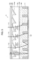
- FIG. 3 is a schematic cross-sectional view of a reflection-type liquid crystal display device according to the present invention.
- FIG. 4 is a schematic cross-sectional view of a reflection-type liquid crystal display device according to the present invention.
- FIG. 5 is a schematic cross-sectional view of a reflection-type liquid crystal display device according to the present invention.
- FIG. 6 is a schematic cross-sectional view of a transmission-type liquid crystal display device according to the present invention.
- FIG. 7 is a schematic cross-sectional view of a transmission-type liquid crystal display device according to the present invention.
- FIG. 8 is a schematic cross-sectional view of a transmission-type liquid crystal display device according to the present invention.
- FIG. 9 is a partial pan view of the display device shown in FIG. 1 .
- the lower substrate may be transparent, each light reflection portion may be a light reflection film laminated on the lower substrate and each light absorption portion may be a light absorption wall perpendicularly embedded into the lower substrate.
- the light absorption wall may be made of a black resin.
- Each light reflection portion may be a light interference film.
- Each protruding portion may define a prism having a triangular cross section. Adjacent two of the protruding portions may define a prism having an isosceles triangular cross section or a trapezoid cross section.
- the display device may include a diffused-vertical light transfer plate, the plate being laid on the upper substrate.
- nematic liquid crystals having refractive index anisotropy can be applied to the liquid crystal layer.
- Materials of the upper and lower substrates of the present invention include not only glass but plastic made of polyether sulfone, polyethylene terephthalate, polycarbonate, epoxy resin, acrylic resin and the like.
- the light reflection portions may be made of aluminum or silver of high refractivity and the light absorption portions may be made of chrome or nickel of low refractivity, and both may be formed into films by sputtering, evaporation or plating. One of them may be formed on another film, or both films may be formed on the same plane. They a may be re provided only to necessary regions through the steps of applying a photosensitive resist, light exposure, development, etching and removal of the resist.
- the light absorption portions can be made of a resist of a black resin.
- the diffused-vertical light transfer plate is, for example, a fiber plate or a microlens made of transparent materials such as glass (non-alkali glass, quartz, etc.), plastic, resin and crystal.
- a fiber plate 194HMF Mitsubishi Rayon Co. Ltd.
- a planar microlens PML or EML Nippon Sheet Glass Co., Ltd.
- the light interference film of the present invention may be made by laminating a plurality of layers each having a light wavelength order thickness. Reflection lights from the upper and the lower surfaces of the layered structure are interfered with each other so that colored reflection lights are observed (Bragg reflection is utilized).
- the light interference film may be formed by “interfering light exposure” in which lights each having a wavelength corresponding to that required by a photo-curing resin are cast from two directions with respect to the substrate.
- Materials thereof include a hologram recording film HRF 700X manufactured by Dupont containing a binder polymer, an acrylate monomer and a polymerization initiator.
- Materials of the light absorption wall of the present invention include a carbon black, a mixture of a carbon black and a resin such as an acrylic resin, a black resist or the like.
- FIGS. 1 and 9 are a schematic cross-sectional view and a partial plan view of a reflection-type liquid crystal display device according to the present invention.
- a reflection-type liquid crystal display device 1 includes a transparent upper substrate 103 having serrated protruding portions thereon and a transparent flat lower substrate 106 .
- the upper substrate 103 has transparent upper electrodes 104 a arranged on the protruding portions and the lower substrate 106 has transparent lower electrodes 104 b crossing the upper electrodes 104 a so that crossing parts of electrodes 104 a and 104 b define pixels P (FIG. 9 ).
- Each protruding portion of the upper substrate 103 has a surface downwardly inclined to define a prism.
- the lower substrate 106 has light reflection portions 107 and light absorption portions 108 on its lower surface.
- a liquid crystal layer 105 is sandwiched between the upper substrate 103 and the lower substrate 106 .
- liquid crystal molecules in the liquid crystal layer 105 are changed between a state in which the liquid crystal molecules are aligned perpendicular to the lower substrate 106 and a state in which the liquid crystal molecules are aligned parallel to the lower substrate 106 .
- the liquid crystal molecules are aligned parallel to the lower substrate 106 , the light is deflected through the upper and lower substrates having the refractive index ng and the liquid crystal layer having the refractive index (ne+no)/2 as indicated by an optical path 110 . Then, the light goes to the light absorption portion 108 so that the light is absorbed and not irradiated to the outside.
- the refractive index of the liquid crystal is continuously controlled by the electric field so that a half tone display can be realized by adjusting an incident light amount ratio between the light reflection portions and the light absorption portions.
- this liquid crystal display device 1 When this liquid crystal display device 1 is used as a reflection-type projector element or the like, since the incident angle of light to the display device 1 is preliminarily set constant, it is sufficient for the liquid crystal display device to control angles of the incident light and the irradiated light by using the above-mentioned constitution.
- this liquid crystal display device when this liquid crystal display device is used as a direct-viewing reflection-type liquid crystal display device, it is preferable to arrange a diffused-vertical light transfer plate 102 on an upper surface of the upper substrate 103 . Further, it is preferable to arrange a light diffusion plate 101 on the diffused-vertical light transfer plate 102 to enhance visual angle characteristics.
- the light diffusion plate 101 is made of a transparent material such as glass, polyester, polycarbonate, polyolefin, polyether sulfone, polyethylene terephthalate, polyacrylate, epoxy resin or the like, and has a surface with irregularities in micron to submicron order.
- the orientation of the liquid crystal may be in a random state. In this case, however, a defect occurs and this defect gives rise to a problem that the light is scattered. Accordingly, in such a case, a small amount of chiral agent may preferably be added to the liquid crystal so as to make the liquid crystal have a helical structure. Further, by coating liquid crystal orientation films on the upper and lower substrates 103 , 106 and then applying rubbing or irradiation of light to the liquid crystal orientation films, it may be possible to give a uniaxial property to the liquid crystal molecules when they are arranged parallel to the lower substrate 106 .
- each light absorption portion 108 on which the light is incident in the dark state can be shared by two pixels. Accordingly, theoretically, the aperture ratio can be increased up to 67%.
- each light absorption portion 111 is configured to a wall standing perpendicularly in the lower substrate 106 as shown in FIG. 3.
- a higher aperture ratio can be obtained using such a constitution.
- the incident light take three optical paths before it is absorbed by the wall 111 . That is, the incident light going along an optical path 112 is once reflected by the reflection portion 107 , and then is absorbed by a side surface of the wall 111 .
- the incident light going along an optical path 113 is irradiated through the liquid crystal layer 105 and is directly absorbed by the side surface of the wall 111 .
- the incident light going along an optical path 114 is irradiated through the liquid crystal layer 105 and is directly absorbed by an upper surface of the wall 111 . Due to such a constitution, an inclination angle of the prisms can be made small so that the thickness of the liquid crystal layer 105 can be made thinner, and so that the uniform orientation of the liquid crystal can be further enhanced.
- the number of the walls 111 can be reduced to one half of that of the constitution shown in FIG. 3 .
- a white and black display having higher brightness and a higher contrast ratio can be obtained.
- a color filter may be arranged behind or in front of the liquid crystal layer.
- FIG. 6 is a schematic cross-sectional view of the transmission-type liquid crystal display device according to the present invention.
- the constitution of the display device 6 is substantially the same as that of the reflection-type liquid crystal display device 1 shown in FIG. 1 .
- targets to be irradiated with the light are changed between light transmission portions 117 and light absorption portion 118 by applying an electric field to the liquid crystal layer 105 .
- the refractive index of the liquid crystal layer 105 can be continuously controlled by adjusting the electric field and hence, a half tone display can be realized by adjusting the incident light amount ratio between the light transmission portions 117 and the light absorption portions 118 .
- the display device 6 When the display device 6 is used as a transmission-type projector element or the like, since the incident angle of light to the display device 6 is preliminarily set constant, it is sufficient for the display device 6 to control angles of the incident light and the irradiated light by using the above-mentioned constitution.
- this liquid crystal display device when this liquid crystal display device is used as a direct-viewing transmission-type liquid crystal display device, it is preferable to arrange a diffused-vertical light transfer plate 116 on an upper surface of the upper substrate 103 . Further, it is effective to arrange a directional film which conforms with the purpose at the light irradiating side (viewer side) to enhance the visual angle characteristics.
- the light absorption portions adopt vertical walls 111 to the substrate to enhance the aperture ratio.
- FIG. 5 An embodiment related to the reflection-type liquid crystal display device is explained using the schematic cross-sectional view of FIG. 5 .
- the pixel pitch P 1 is 100 ⁇ m and the width W 1 of the aperture portions is 80 ⁇ m (with an aperture ratio of 80%).
- V-shaped protrusions i.e.
- Such a structure of the upper-substrate 103 can be produced by cutting a glass substrate, and also the structure can be obtained by molding an acrylic resin using a metallic mold.
- the thickness T 1 of the liquid crystal layer is set to 18 ⁇ m.
- the transparent electrodes 104 a , 104 b are made of ITO (Indium Tin Oxide). With respect to the transparent electrodes 104 a , 104 b , only on the surface the transparent electrodes 104 b of the lower substrate 106 , a horizontal orientation film is coated and subjected to a rubbing treatment. Although a slight defect of disclination line may be observed when the electric field is not applied, an approximately uniform orientation state is obtained. Further, since the cholestric helical pitch is several ⁇ m to several tens of ⁇ m, coloring due to selective reflection is not observed.
- ITO Indium Tin Oxide
- the liquid crystal used here may be a material having a negative dielectric anisotropy.
- a vertical orientation film is used as an orientation film, since at least one of the upper and lower substrates 103 , 106 adopts inclined surfaces, there is no irregularities of the orientation at the time of applying the electric field and hence, it is unnecessary to provide an orientation treatment such as rubbing or the like.
- black resins having a width W 2 of 20 ⁇ m of the upper substrate 103 , black resins (light absorption walls) having a width W 2 of 20 ⁇ m and a height H 2 of 340 ⁇ m are embedded in the lower substrate 106 to define the wall 111 at a pitch P 1 of 100 ⁇ m.
- This structure of the lower substrate 106 is obtained by digging a glass substrate to form grooves having a width of 20 ⁇ m and a depth of 340 ⁇ m by sand blasting and then by injecting a ultraviolet ray curable black resin in the grooves and thereafter by performing a ultraviolet ray irradiation to cure the black resin using a patterned mask.
- the digging of the glass substrate may be performed by an abrasion method using an excimer laser, a dry etching method and an ion milling method.
- transparent silicon resin films having a thickness corresponding to the size and pitch of the pixels P and thin films (for example, aluminum films) having both surfaces coated in black and a thickness corresponding to that of the wall are alternately laminated, then they are subjected to a heat pressing by a lamination processing to be changed to a panel, then the panel are sliced in the direction perpendicular to the laminating direction so as to obtain the lower substrate 106 having light absorption walls 111 which penetrate in the panel cross-sectional direction.
- an optical fiber plate is arranged on an upper surface of the substrate as the diffused-vertical light transfer plate 102 and the light diffusion plate 101 is arranged on the optical fiber plate.
- the light incident on the lower substrate 106 from the liquid crystal layer 105 is irradiated at an inclination angle of approximately 1.6° to closer one of the black walls 111 .
- substantially the whole incident light is absorbed by the black walls 111 by way of the deflected optical paths shown in FIG. 5 and hence, the dark state is obtained.
- the liquid crystal molecules are oriented perpendicular to the lower substrate 106 and the incident light is reflected toward the viewer side so that the bright state having the high brightness is obtained.
- a second embodiment which relates to the reflection-type liquid crystal display device is explained in conjunction with the schematic cross-sectional view shown in FIG. 4 .
- each prism is formed such that a right-angled triangular shaped protruding portion having a width of 80 ⁇ m at the aperture portion (a short side of a trapezoid defined when two pixels are considered to be coupled) is protruded in the liquid crystal layer 105 from the upper substrate 103 .
- the prism has a height H 1 of 40 ⁇ m and an inclination angle ⁇ of 26.5°.
- the thickness T 1 of the liquid crystal layer 105 is set to 50 ⁇ m.
- the light absorption wall 111 having a width W 1 of 20 ⁇ m and a height H 2 of 535 ⁇ m is embedded at a pitch P 2 of 200 ⁇ m in the lower substrate 106 .
- the liquid crystal molecules Due to such a constitution, in the state that the liquid crystal is orientated parallel to the lower substrate 106 , the light is completely incident on the light absorption walls 111 and the dark state which prevents the light from being irradiated to the viewer is obtained. Further, when a sufficient electric field is applied, the liquid crystal molecules are oriented in the direction perpendicular to the lower substrate 106 and the incident light is reflected to the viewer side so that the bright state having the high brightness is obtained.
- each prism is formed such that a V-shaped protruding portion having a width W 1 of 80 ⁇ m at the aperture portion is protruded in the liquid crystal layer 105 from the upper substrate 103 .
- the prism has a height H 1 of 15.4 ⁇ m and a inclination angle ⁇ of 21°.
- the thickness T 1 of the liquid crystal layer 105 is set to 20 ⁇ m.
- the light absorption wall 111 having a width W 2 of 20 ⁇ m and a height H 2 of 560 ⁇ m is embedded at a pitch P 1 of 100 ⁇ m in the lower substrate 106 .
- the liquid crystal molecules Due to such a constitution, in the state that the liquid crystal is orientated parallel to the lower substrate 106 , the light is completely incident on the light absorption walls 11 and the dark state which prevents the light from being irradiated to the viewer side is obtained. Further, when a sufficient electric field is applied, the liquid crystal molecules are oriented in the direction perpendicular to the substrate 106 , the incident light reaches the light transmission portion so that a bright state having high brightness is obtained.
- a second embodiment which relates to the transmission-type liquid crystal display device of the present invention is explained in conjunction with the schematic cross-sectional view shown in FIG. 7 .
- each prism portion is formed such that a right-angled triangular shaped protruding portion having a width H 1 of 80 ⁇ m at the aperture portion (a short side of a trapezoid defined when two pixels are considered to be coupled) is protruded in the liquid crystal layer 105 from the upper substrate 103 .
- the prism has a height H 1 of 63 ⁇ m and an inclination angle ⁇ of 38°.
- the thickness T 1 of the liquid crystal layer 105 is set to 70 ⁇ m.
- the light absorption wall 111 having a width W 2 of 20 ⁇ m and a height H 2 of 830 ⁇ m is embedded at a pitch P 2 of 200 ⁇ m in the lower substrate 106 .
- the liquid crystal molecules Due to such a constitution, in the state that the liquid crystal is orientated parallel to the lower substrate 106 , the light is completely incident on the light absorption walls 111 and the dark state which prevents the light from being irradiated to the viewer side is obtained. Further, when the sufficient electric field is applied, the liquid crystal molecules are oriented in the direction perpendicular to the lower substrate 106 , the incident light reaches the light transmission portion so that the bright state having a high brightness is obtained.
- the constitution without a polarizer or with a single polarizer can realize high brightness and contrast in which by applying an electric field to the liquid crystal layer, the optical path of the irradiated light after passing the liquid crystal layer is changed between the light reflection portions (or the light transmission portions) and the light absorption portions.
- the higher brightness can be realized.
- the liquid crystal display device of the invention is applicable to the reflection-type and the transmission-type direct-viewing liquid crystal displays, the projection-type liquid crystal projectors, the optical information processing devices and the like.
Applications Claiming Priority (3)
| Application Number | Priority Date | Filing Date | Title |
|---|---|---|---|
| JP35527499A JP3524831B2 (ja) | 1999-12-15 | 1999-12-15 | 反射型および透過型液晶表示装置 |
| JP11-355274 | 1999-12-15 | ||
| JPHEI11-355274 | 1999-12-15 |
Publications (2)
| Publication Number | Publication Date |
|---|---|
| US20010004279A1 US20010004279A1 (en) | 2001-06-21 |
| US6657700B2 true US6657700B2 (en) | 2003-12-02 |
Family
ID=18442980
Family Applications (1)
| Application Number | Title | Priority Date | Filing Date |
|---|---|---|---|
| US09/736,202 Expired - Lifetime US6657700B2 (en) | 1999-12-15 | 2000-12-15 | Reflection-type and transmission-type liquid crystal display devices |
Country Status (2)
| Country | Link |
|---|---|
| US (1) | US6657700B2 (ja) |
| JP (1) | JP3524831B2 (ja) |
Cited By (20)
| Publication number | Priority date | Publication date | Assignee | Title |
|---|---|---|---|---|
| US20020101552A1 (en) * | 2001-02-01 | 2002-08-01 | Jong-Hoon Yi | Transflective liquid crystal display device having a color filter and method for fabricating thereof |
| US20030076472A1 (en) * | 2001-09-28 | 2003-04-24 | Hoya Corporation | Opposite substrate for liquid crystal display panel, and medthod of fabricating the same |
| US20040196411A1 (en) * | 2003-04-03 | 2004-10-07 | Nokia Corporation | Direct view display based on light diffraction from a deformable layer |
| US20050018307A1 (en) * | 2003-07-16 | 2005-01-27 | Seiko Epson Corporation | Spatial light modulator and projector |
| US20050140872A1 (en) * | 2003-12-30 | 2005-06-30 | Lg Philips Lcd Co., Ltd. | Transflective type liquid crystal display device and method for manufactruing the same |
| US20070200975A1 (en) * | 2006-02-14 | 2007-08-30 | Seiko Epson Corporation | Electro-optic device, method for manufacturing electro-optic device, projector, and electronic apparatus |
| US20090257108A1 (en) * | 2008-04-15 | 2009-10-15 | Qualcomm Mems Technologies, Inc. | Light with bi-directional propagation |
| US20100309103A1 (en) * | 2004-09-27 | 2010-12-09 | Qualcomm Mems Technologies, Inc. | Methods and devices for lighting displays |
| US7933475B2 (en) | 2006-02-17 | 2011-04-26 | Qualcomm Mems Technologies, Inc. | Method and apparatus for providing back-lighting in a display device |
| US7986451B2 (en) * | 2004-09-27 | 2011-07-26 | Qualcomm Mems Technologies, Inc. | Optical films for directing light towards active areas of displays |
| US8040588B2 (en) | 2004-09-27 | 2011-10-18 | Qualcomm Mems Technologies, Inc. | System and method of illuminating interferometric modulators using backlighting |
| US8045252B2 (en) | 2004-02-03 | 2011-10-25 | Qualcomm Mems Technologies, Inc. | Spatial light modulator with integrated optical compensation structure |
| US8172417B2 (en) | 2009-03-06 | 2012-05-08 | Qualcomm Mems Technologies, Inc. | Shaped frontlight reflector for use with display |
| US8344377B2 (en) | 2004-09-27 | 2013-01-01 | Qualcomm Mems Technologies, Inc. | Display element having filter material diffused in a substrate of the display element |
| US8798425B2 (en) | 2007-12-07 | 2014-08-05 | Qualcomm Mems Technologies, Inc. | Decoupled holographic film and diffuser |
| US8848294B2 (en) | 2010-05-20 | 2014-09-30 | Qualcomm Mems Technologies, Inc. | Method and structure capable of changing color saturation |
| US8872085B2 (en) | 2006-10-06 | 2014-10-28 | Qualcomm Mems Technologies, Inc. | Display device having front illuminator with turning features |
| US8979349B2 (en) | 2009-05-29 | 2015-03-17 | Qualcomm Mems Technologies, Inc. | Illumination devices and methods of fabrication thereof |
| US9019183B2 (en) | 2006-10-06 | 2015-04-28 | Qualcomm Mems Technologies, Inc. | Optical loss structure integrated in an illumination apparatus |
| US9025235B2 (en) | 2002-12-25 | 2015-05-05 | Qualcomm Mems Technologies, Inc. | Optical interference type of color display having optical diffusion layer between substrate and electrode |
Families Citing this family (21)
| Publication number | Priority date | Publication date | Assignee | Title |
|---|---|---|---|---|
| US6867888B2 (en) * | 1996-07-12 | 2005-03-15 | Science Applications International Corporation | Switchable polymer-dispersed liquid crystal optical elements |
| IL136248A (en) * | 2000-05-21 | 2004-08-31 | Elop Electrooptics Ind Ltd | System and method for changing light transmission through a substrate |
| JP4022096B2 (ja) * | 2002-05-02 | 2007-12-12 | 株式会社リコー | 光偏向素子及び画像表示装置 |
| JP4400027B2 (ja) * | 2002-07-11 | 2010-01-20 | セイコーエプソン株式会社 | 半透過・反射型電気光学装置、およびそれを用いた電子機器 |
| AU2002313512A1 (en) * | 2002-08-21 | 2004-03-11 | Nokia Corporation | Switchable lens display |
| US6950173B1 (en) | 2003-04-08 | 2005-09-27 | Science Applications International Corporation | Optimizing performance parameters for switchable polymer dispersed liquid crystal optical elements |
| JP2005055620A (ja) * | 2003-08-01 | 2005-03-03 | Canon Inc | 反射型表示素子 |
| US7059719B2 (en) * | 2003-09-02 | 2006-06-13 | University Of Pittsburagh - Of The Commonwealth System Of Higher Education | Contact lenses colored with crystalline colloidal array technology |
| TWI351549B (en) * | 2004-09-03 | 2011-11-01 | Hon Hai Prec Ind Co Ltd | Backlight module capable of emitting light from tw |
| KR100709985B1 (ko) * | 2005-01-04 | 2007-04-23 | 삼성코닝 주식회사 | 디스플레이 장치용 필터 및 이를 포함한 디스플레이 장치 |
| US7605538B2 (en) * | 2005-06-10 | 2009-10-20 | Lg Electronics Inc. | Plasma display panel |
| KR100709221B1 (ko) * | 2005-08-18 | 2007-04-18 | 삼성에스디아이 주식회사 | 가요성 표시 장치 |
| KR101301561B1 (ko) * | 2005-11-29 | 2013-09-04 | 크리에이터 테크놀로지 비.브이. | 말릴 수 있는 디스플레이를 위한 칼러 필터 |
| KR20130121545A (ko) * | 2012-04-27 | 2013-11-06 | 삼성디스플레이 주식회사 | 표시 장치 및 그 제조 방법 |
| KR20150043391A (ko) * | 2012-08-13 | 2015-04-22 | 바이엘 머티리얼사이언스 아게 | 아웃-커플링 부재를 갖는 도광판 |
| KR102057970B1 (ko) * | 2013-08-01 | 2019-12-23 | 삼성디스플레이 주식회사 | 표시 장치 및 그 제조 방법 |
| JP2018054639A (ja) * | 2015-02-13 | 2018-04-05 | パナソニックIpマネジメント株式会社 | 光学デバイス |
| KR20180034007A (ko) * | 2016-09-27 | 2018-04-04 | 삼성전자주식회사 | 디스플레이 장치 |
| WO2018105312A1 (ja) * | 2016-12-06 | 2018-06-14 | Jnc株式会社 | 液晶複合体および液晶調光素子 |
| CN106990596A (zh) * | 2017-05-12 | 2017-07-28 | 武汉华星光电技术有限公司 | 彩膜基板和液晶显示器 |
| CN109976022B (zh) * | 2019-04-30 | 2022-04-19 | 京东方科技集团股份有限公司 | 一种像素结构及其制备方法、显示面板 |
Citations (19)
| Publication number | Priority date | Publication date | Assignee | Title |
|---|---|---|---|---|
| WO1983001016A1 (en) | 1981-09-16 | 1983-03-31 | R & D Partnership Manchester | Encapsulated liquid crystal and method |
| US4389096A (en) * | 1977-12-27 | 1983-06-21 | Matsushita Electric Industrial Co., Ltd. | Image display apparatus of liquid crystal valve projection type |
| US4729640A (en) * | 1984-10-03 | 1988-03-08 | Canon Kabushiki Kaisha | Liquid crystal light modulation device |
| US5220444A (en) | 1990-07-17 | 1993-06-15 | Sharp Kabushiki Kaisha | Reflective-type liquid crystal display device with etched oxide layer between substrate and metal film and method for producing same |
| JPH06317702A (ja) | 1993-05-07 | 1994-11-15 | Fujitsu Ltd | 表示補助用片面反射板および液晶表示装置 |
| JPH0792507A (ja) | 1993-07-28 | 1995-04-07 | Nippon Telegr & Teleph Corp <Ntt> | 液晶マイクロプリズムアレイ及びそれを用いた空間光ビーム接続器と光スイッチ |
| JPH0887006A (ja) | 1994-09-19 | 1996-04-02 | Toshiba Corp | 液晶表示装置 |
| JPH0897006A (ja) | 1994-09-29 | 1996-04-12 | Taiyo Yuden Co Ltd | チップ状セラミック電子部品及びその製造方法 |
| JPH08114797A (ja) | 1994-10-14 | 1996-05-07 | Seiko Epson Corp | 反射型液晶表示装置およびその製造方法 |
| US5559617A (en) | 1993-07-30 | 1996-09-24 | Sharp Kabushiki Kaisha | Liquid crystal display device with overlapping compensators with portions having different retardation values |
| JPH09152579A (ja) | 1995-09-26 | 1997-06-10 | Denso Corp | 屈折型液晶素子 |
| US5684551A (en) | 1992-06-26 | 1997-11-04 | Sharp Kabushiki Kaisha | Reflective type liquid crystal display device with phase compensator and reflector with undulating surface |
| US5691791A (en) | 1993-07-30 | 1997-11-25 | Sharp Kabushiki Kaisha | Reflective liquid crystal display device and reflector |
| JPH1062778A (ja) | 1996-08-20 | 1998-03-06 | Matsushita Electric Ind Co Ltd | 反射型液晶表示装置 |
| JP2724596B2 (ja) | 1987-10-20 | 1998-03-09 | 大日本インキ化学工業株式会社 | 液晶デバイス及びその製造方法 |
| JPH10253954A (ja) * | 1997-03-14 | 1998-09-25 | Matsushita Electric Ind Co Ltd | 反射型液晶表示装置 |
| US6108064A (en) | 1997-11-06 | 2000-08-22 | Sharp Kabushiki Kaisha | Reflective-type liquid crystal display device including a single polarizer plate |
| US6323970B1 (en) * | 1999-09-29 | 2001-11-27 | Digilents, Inc. | Method of producing switchable holograms |
| US6331878B1 (en) * | 1994-07-20 | 2001-12-18 | Matsushita Electric Industrial Co., Ltd. | Reflection light absorbing plate and display panel for use in a display apparatus |
-
1999
- 1999-12-15 JP JP35527499A patent/JP3524831B2/ja not_active Expired - Fee Related
-
2000
- 2000-12-15 US US09/736,202 patent/US6657700B2/en not_active Expired - Lifetime
Patent Citations (21)
| Publication number | Priority date | Publication date | Assignee | Title |
|---|---|---|---|---|
| US4389096A (en) * | 1977-12-27 | 1983-06-21 | Matsushita Electric Industrial Co., Ltd. | Image display apparatus of liquid crystal valve projection type |
| JPS58501631A (ja) | 1981-09-16 | 1983-09-29 | マンチェスタ・ア−ル・アンド・ディ・パ−トナ−シップ | 液晶構成体と液晶光学装置 |
| WO1983001016A1 (en) | 1981-09-16 | 1983-03-31 | R & D Partnership Manchester | Encapsulated liquid crystal and method |
| US4729640A (en) * | 1984-10-03 | 1988-03-08 | Canon Kabushiki Kaisha | Liquid crystal light modulation device |
| JP2724596B2 (ja) | 1987-10-20 | 1998-03-09 | 大日本インキ化学工業株式会社 | 液晶デバイス及びその製造方法 |
| US5220444A (en) | 1990-07-17 | 1993-06-15 | Sharp Kabushiki Kaisha | Reflective-type liquid crystal display device with etched oxide layer between substrate and metal film and method for producing same |
| US5684551A (en) | 1992-06-26 | 1997-11-04 | Sharp Kabushiki Kaisha | Reflective type liquid crystal display device with phase compensator and reflector with undulating surface |
| US5847789A (en) | 1992-06-26 | 1998-12-08 | Sharp Kabushiki Kaisha | Reflective type liquid crystal display device |
| JPH06317702A (ja) | 1993-05-07 | 1994-11-15 | Fujitsu Ltd | 表示補助用片面反射板および液晶表示装置 |
| JPH0792507A (ja) | 1993-07-28 | 1995-04-07 | Nippon Telegr & Teleph Corp <Ntt> | 液晶マイクロプリズムアレイ及びそれを用いた空間光ビーム接続器と光スイッチ |
| US5559617A (en) | 1993-07-30 | 1996-09-24 | Sharp Kabushiki Kaisha | Liquid crystal display device with overlapping compensators with portions having different retardation values |
| US5691791A (en) | 1993-07-30 | 1997-11-25 | Sharp Kabushiki Kaisha | Reflective liquid crystal display device and reflector |
| US6331878B1 (en) * | 1994-07-20 | 2001-12-18 | Matsushita Electric Industrial Co., Ltd. | Reflection light absorbing plate and display panel for use in a display apparatus |
| JPH0887006A (ja) | 1994-09-19 | 1996-04-02 | Toshiba Corp | 液晶表示装置 |
| JPH0897006A (ja) | 1994-09-29 | 1996-04-12 | Taiyo Yuden Co Ltd | チップ状セラミック電子部品及びその製造方法 |
| JPH08114797A (ja) | 1994-10-14 | 1996-05-07 | Seiko Epson Corp | 反射型液晶表示装置およびその製造方法 |
| JPH09152579A (ja) | 1995-09-26 | 1997-06-10 | Denso Corp | 屈折型液晶素子 |
| JPH1062778A (ja) | 1996-08-20 | 1998-03-06 | Matsushita Electric Ind Co Ltd | 反射型液晶表示装置 |
| JPH10253954A (ja) * | 1997-03-14 | 1998-09-25 | Matsushita Electric Ind Co Ltd | 反射型液晶表示装置 |
| US6108064A (en) | 1997-11-06 | 2000-08-22 | Sharp Kabushiki Kaisha | Reflective-type liquid crystal display device including a single polarizer plate |
| US6323970B1 (en) * | 1999-09-29 | 2001-11-27 | Digilents, Inc. | Method of producing switchable holograms |
Cited By (39)
| Publication number | Priority date | Publication date | Assignee | Title |
|---|---|---|---|---|
| US8253893B2 (en) | 2001-02-01 | 2012-08-28 | Lg Display Co., Ltd. | Transflective liquid crystal display device having a color filter and method for fabricating thereof |
| US6809791B2 (en) * | 2001-02-01 | 2004-10-26 | Lg.Philips Lcd Co., Ltd. | Transflective liquid crystal display device having a color filter and method for fabricating thereof |
| US20050046769A1 (en) * | 2001-02-01 | 2005-03-03 | Lg. Philips Lcd Co., Ltd. | Transflective liquid crystal display device having a color filter and method for fabricating thereof |
| US20080036950A1 (en) * | 2001-02-01 | 2008-02-14 | Jong-Huon Yi | Transflective liquid crystal display device having a color filter and method for fabricating thereof |
| US20020101552A1 (en) * | 2001-02-01 | 2002-08-01 | Jong-Hoon Yi | Transflective liquid crystal display device having a color filter and method for fabricating thereof |
| US20100149466A1 (en) * | 2001-02-01 | 2010-06-17 | Jong-Hoon Yi | Transflective liquid crystal display device having a color filter and method for fabricating thereof |
| US7697092B2 (en) | 2001-02-01 | 2010-04-13 | Lg Display Co., Ltd. | Transflective liquid crystal display device having a color filter and method for fabricating thereof |
| US7265808B2 (en) | 2001-02-01 | 2007-09-04 | Lg.Philips Lcd Co., Ltd | Transflective liquid crystal display device having a color filter and method for fabricating thereof |
| US20030076472A1 (en) * | 2001-09-28 | 2003-04-24 | Hoya Corporation | Opposite substrate for liquid crystal display panel, and medthod of fabricating the same |
| US6917402B2 (en) * | 2001-09-28 | 2005-07-12 | Hoya Corporation | Opposite substrate for liquid crystal display panel with particular microlenses and layered light shields, and method of fabricating the same |
| US9025235B2 (en) | 2002-12-25 | 2015-05-05 | Qualcomm Mems Technologies, Inc. | Optical interference type of color display having optical diffusion layer between substrate and electrode |
| US20040196411A1 (en) * | 2003-04-03 | 2004-10-07 | Nokia Corporation | Direct view display based on light diffraction from a deformable layer |
| US7050126B2 (en) * | 2003-04-03 | 2006-05-23 | Nokia Corporation | Direct view display based on light diffraction from a deformable layer |
| US20060203349A1 (en) * | 2003-07-16 | 2006-09-14 | Seiko Epson Corporation | Spatial light modulator and projector |
| US20050018307A1 (en) * | 2003-07-16 | 2005-01-27 | Seiko Epson Corporation | Spatial light modulator and projector |
| US7113341B2 (en) * | 2003-07-16 | 2006-09-26 | Seiko Epson Corporation | Spatial light modulator and projector |
| US7327519B2 (en) | 2003-07-16 | 2008-02-05 | Seiko Epson Corporation | Spatial light modulator and projector |
| US7365814B2 (en) * | 2003-12-30 | 2008-04-29 | Lg. Philips Lcd Co., Ltd | Transflective type liquid crystal display device |
| US20050140872A1 (en) * | 2003-12-30 | 2005-06-30 | Lg Philips Lcd Co., Ltd. | Transflective type liquid crystal display device and method for manufactruing the same |
| US8045252B2 (en) | 2004-02-03 | 2011-10-25 | Qualcomm Mems Technologies, Inc. | Spatial light modulator with integrated optical compensation structure |
| US9019590B2 (en) | 2004-02-03 | 2015-04-28 | Qualcomm Mems Technologies, Inc. | Spatial light modulator with integrated optical compensation structure |
| US8111445B2 (en) | 2004-02-03 | 2012-02-07 | Qualcomm Mems Technologies, Inc. | Spatial light modulator with integrated optical compensation structure |
| US7986451B2 (en) * | 2004-09-27 | 2011-07-26 | Qualcomm Mems Technologies, Inc. | Optical films for directing light towards active areas of displays |
| US8013831B2 (en) | 2004-09-27 | 2011-09-06 | Qualcomm Mems Technologies, Inc. | Methods and devices for lighting displays |
| US8040588B2 (en) | 2004-09-27 | 2011-10-18 | Qualcomm Mems Technologies, Inc. | System and method of illuminating interferometric modulators using backlighting |
| US20100309103A1 (en) * | 2004-09-27 | 2010-12-09 | Qualcomm Mems Technologies, Inc. | Methods and devices for lighting displays |
| US8344377B2 (en) | 2004-09-27 | 2013-01-01 | Qualcomm Mems Technologies, Inc. | Display element having filter material diffused in a substrate of the display element |
| US20070200975A1 (en) * | 2006-02-14 | 2007-08-30 | Seiko Epson Corporation | Electro-optic device, method for manufacturing electro-optic device, projector, and electronic apparatus |
| US7693389B2 (en) * | 2006-02-14 | 2010-04-06 | Seiko Epson Corporation | Electro-optic device, method for manufacturing electro-optic device, projector, and electronic apparatus |
| US7933475B2 (en) | 2006-02-17 | 2011-04-26 | Qualcomm Mems Technologies, Inc. | Method and apparatus for providing back-lighting in a display device |
| US8872085B2 (en) | 2006-10-06 | 2014-10-28 | Qualcomm Mems Technologies, Inc. | Display device having front illuminator with turning features |
| US9019183B2 (en) | 2006-10-06 | 2015-04-28 | Qualcomm Mems Technologies, Inc. | Optical loss structure integrated in an illumination apparatus |
| US8798425B2 (en) | 2007-12-07 | 2014-08-05 | Qualcomm Mems Technologies, Inc. | Decoupled holographic film and diffuser |
| US8049951B2 (en) | 2008-04-15 | 2011-11-01 | Qualcomm Mems Technologies, Inc. | Light with bi-directional propagation |
| US20090257108A1 (en) * | 2008-04-15 | 2009-10-15 | Qualcomm Mems Technologies, Inc. | Light with bi-directional propagation |
| US8172417B2 (en) | 2009-03-06 | 2012-05-08 | Qualcomm Mems Technologies, Inc. | Shaped frontlight reflector for use with display |
| US8979349B2 (en) | 2009-05-29 | 2015-03-17 | Qualcomm Mems Technologies, Inc. | Illumination devices and methods of fabrication thereof |
| US9121979B2 (en) | 2009-05-29 | 2015-09-01 | Qualcomm Mems Technologies, Inc. | Illumination devices and methods of fabrication thereof |
| US8848294B2 (en) | 2010-05-20 | 2014-09-30 | Qualcomm Mems Technologies, Inc. | Method and structure capable of changing color saturation |
Also Published As
| Publication number | Publication date |
|---|---|
| JP3524831B2 (ja) | 2004-05-10 |
| US20010004279A1 (en) | 2001-06-21 |
| JP2001174801A (ja) | 2001-06-29 |
Similar Documents
| Publication | Publication Date | Title |
|---|---|---|
| US6657700B2 (en) | Reflection-type and transmission-type liquid crystal display devices | |
| JP3351945B2 (ja) | 反射型液晶表示装置 | |
| US5877829A (en) | Liquid crystal display apparatus having adjustable viewing angle characteristics | |
| JP3852342B2 (ja) | 反射板、反射板の製造方法、液晶装置、電子機器 | |
| KR100272875B1 (ko) | 확산도광판,백라이트소스및이를사용한액정표시장치 | |
| KR100474057B1 (ko) | 액정표시소자 | |
| US20050264730A1 (en) | Liquid crystal display and method of manufacturing the same | |
| KR20020002248A (ko) | 액정표시소자 및 그 제조방법 | |
| KR20020077220A (ko) | 액정 표시 장치 | |
| KR100695698B1 (ko) | 디스플레이 디바이스, 보상 필름 및 액정 디스플레이 | |
| JP3072513B2 (ja) | 高分子分散型液晶表示パネル | |
| JP2006293393A (ja) | 反射板、反射板の製造方法、液晶装置、電子機器 | |
| US6072553A (en) | Reflection-type liquid crystal display with layer comprising liquid crystal compound and liquid crystal polymer being twist-aligned at same angle | |
| JP3557313B2 (ja) | 液晶表示スクリーン | |
| KR101356272B1 (ko) | 고분자 분산형 액정 표시장치 및 그 제조 방법 | |
| KR100663074B1 (ko) | 위상차층을 포함하는 반사투과형 액정표시장치 | |
| US6606138B2 (en) | Liquid crystal layer including a dichroic dye | |
| US20010040659A1 (en) | Reflection liquid crystal display device | |
| JPH11160687A (ja) | 表示装置及び光拡散層の製造方法 | |
| JP2001281662A (ja) | 液晶表示装置 | |
| WO2019208260A1 (ja) | 液晶表示装置 | |
| JP4076780B2 (ja) | 液晶表示装置 | |
| JP2000029021A (ja) | 反射型液晶表示装置 | |
| JPH11249128A (ja) | 反射型液晶装置及び電子機器 | |
| JPH07152029A (ja) | 表示素子 |
Legal Events
| Date | Code | Title | Description |
|---|---|---|---|
| AS | Assignment |
Owner name: SHARP KABUSHIKI KAISHA, JAPAN Free format text: ASSIGNMENT OF ASSIGNORS INTEREST;ASSIGNORS:SAKO, TEIYU;MITSUI, SEIICHI;REEL/FRAME:011382/0381 Effective date: 20001127 |
|
| STCF | Information on status: patent grant |
Free format text: PATENTED CASE |
|
| FEPP | Fee payment procedure |
Free format text: PAYOR NUMBER ASSIGNED (ORIGINAL EVENT CODE: ASPN); ENTITY STATUS OF PATENT OWNER: LARGE ENTITY |
|
| FPAY | Fee payment |
Year of fee payment: 4 |
|
| FPAY | Fee payment |
Year of fee payment: 8 |
|
| FPAY | Fee payment |
Year of fee payment: 12 |