US6504198B2 - Horizontal type ferroelectric memory and manufacturing method of the same - Google Patents
Horizontal type ferroelectric memory and manufacturing method of the same Download PDFInfo
- Publication number
- US6504198B2 US6504198B2 US09/816,478 US81647801A US6504198B2 US 6504198 B2 US6504198 B2 US 6504198B2 US 81647801 A US81647801 A US 81647801A US 6504198 B2 US6504198 B2 US 6504198B2
- Authority
- US
- United States
- Prior art keywords
- film
- ferroelectric memory
- ferroelectric
- capacitor
- memory according
- Prior art date
- Legal status (The legal status is an assumption and is not a legal conclusion. Google has not performed a legal analysis and makes no representation as to the accuracy of the status listed.)
- Expired - Fee Related
Links
- 238000004519 manufacturing process Methods 0.000 title abstract description 41
- 239000003990 capacitor Substances 0.000 claims abstract description 110
- 230000004888 barrier function Effects 0.000 claims abstract description 51
- 238000009792 diffusion process Methods 0.000 claims abstract description 38
- 239000000758 substrate Substances 0.000 claims abstract description 20
- 239000004065 semiconductor Substances 0.000 claims abstract description 18
- 239000000463 material Substances 0.000 claims description 22
- 239000010410 layer Substances 0.000 claims description 21
- 229910052697 platinum Inorganic materials 0.000 claims description 15
- 239000011229 interlayer Substances 0.000 claims description 12
- 239000000126 substance Substances 0.000 claims description 11
- 229910021332 silicide Inorganic materials 0.000 claims description 10
- FVBUAEGBCNSCDD-UHFFFAOYSA-N silicide(4-) Chemical compound [Si-4] FVBUAEGBCNSCDD-UHFFFAOYSA-N 0.000 claims description 10
- 150000004767 nitrides Chemical class 0.000 claims description 8
- HTXDPTMKBJXEOW-UHFFFAOYSA-N iridium(IV) oxide Inorganic materials O=[Ir]=O HTXDPTMKBJXEOW-UHFFFAOYSA-N 0.000 claims description 7
- 229910052581 Si3N4 Inorganic materials 0.000 claims description 6
- 229910052741 iridium Inorganic materials 0.000 claims description 6
- HQVNEWCFYHHQES-UHFFFAOYSA-N silicon nitride Chemical compound N12[Si]34N5[Si]62N3[Si]51N64 HQVNEWCFYHHQES-UHFFFAOYSA-N 0.000 claims description 6
- 229910052782 aluminium Inorganic materials 0.000 claims description 2
- 229910052802 copper Inorganic materials 0.000 claims description 2
- 229910052758 niobium Inorganic materials 0.000 claims description 2
- 229910052719 titanium Inorganic materials 0.000 claims description 2
- XUIMIQQOPSSXEZ-UHFFFAOYSA-N Silicon Chemical compound [Si] XUIMIQQOPSSXEZ-UHFFFAOYSA-N 0.000 claims 12
- 229910052710 silicon Inorganic materials 0.000 claims 12
- 239000010703 silicon Substances 0.000 claims 12
- WOCIAKWEIIZHES-UHFFFAOYSA-N ruthenium(iv) oxide Chemical compound O=[Ru]=O WOCIAKWEIIZHES-UHFFFAOYSA-N 0.000 claims 10
- 239000002184 metal Substances 0.000 claims 2
- 229910052751 metal Inorganic materials 0.000 claims 2
- 238000000137 annealing Methods 0.000 abstract description 16
- 230000001590 oxidative effect Effects 0.000 abstract description 11
- 238000000034 method Methods 0.000 description 36
- BASFCYQUMIYNBI-UHFFFAOYSA-N platinum Substances [Pt] BASFCYQUMIYNBI-UHFFFAOYSA-N 0.000 description 20
- 238000005530 etching Methods 0.000 description 16
- 238000010438 heat treatment Methods 0.000 description 8
- WFKWXMTUELFFGS-UHFFFAOYSA-N tungsten Chemical compound [W] WFKWXMTUELFFGS-UHFFFAOYSA-N 0.000 description 7
- 229910052721 tungsten Inorganic materials 0.000 description 7
- 239000010937 tungsten Substances 0.000 description 7
- 238000000151 deposition Methods 0.000 description 6
- 239000000470 constituent Substances 0.000 description 5
- 230000003647 oxidation Effects 0.000 description 5
- 238000007254 oxidation reaction Methods 0.000 description 5
- QVGXLLKOCUKJST-UHFFFAOYSA-N atomic oxygen Chemical compound [O] QVGXLLKOCUKJST-UHFFFAOYSA-N 0.000 description 4
- 230000008901 benefit Effects 0.000 description 4
- 230000015572 biosynthetic process Effects 0.000 description 4
- 238000002955 isolation Methods 0.000 description 4
- 239000001301 oxygen Substances 0.000 description 4
- 229910052760 oxygen Inorganic materials 0.000 description 4
- 239000004020 conductor Substances 0.000 description 3
- 230000008021 deposition Effects 0.000 description 3
- 239000007772 electrode material Substances 0.000 description 3
- 239000012535 impurity Substances 0.000 description 3
- 238000001459 lithography Methods 0.000 description 3
- 238000002161 passivation Methods 0.000 description 3
- 229910021420 polycrystalline silicon Inorganic materials 0.000 description 3
- IJGRMHOSHXDMSA-UHFFFAOYSA-N Atomic nitrogen Chemical compound N#N IJGRMHOSHXDMSA-UHFFFAOYSA-N 0.000 description 2
- 229910052799 carbon Inorganic materials 0.000 description 2
- 239000002131 composite material Substances 0.000 description 2
- 239000010949 copper Substances 0.000 description 2
- 230000001747 exhibiting effect Effects 0.000 description 2
- 239000011810 insulating material Substances 0.000 description 2
- 238000009413 insulation Methods 0.000 description 2
- 238000012986 modification Methods 0.000 description 2
- 230000004048 modification Effects 0.000 description 2
- 239000010955 niobium Substances 0.000 description 2
- 238000011084 recovery Methods 0.000 description 2
- 238000004544 sputter deposition Methods 0.000 description 2
- 239000010936 titanium Substances 0.000 description 2
- RYGMFSIKBFXOCR-UHFFFAOYSA-N Copper Chemical compound [Cu] RYGMFSIKBFXOCR-UHFFFAOYSA-N 0.000 description 1
- UFHFLCQGNIYNRP-UHFFFAOYSA-N Hydrogen Chemical compound [H][H] UFHFLCQGNIYNRP-UHFFFAOYSA-N 0.000 description 1
- RTAQQCXQSZGOHL-UHFFFAOYSA-N Titanium Chemical compound [Ti] RTAQQCXQSZGOHL-UHFFFAOYSA-N 0.000 description 1
- XAGFODPZIPBFFR-UHFFFAOYSA-N aluminium Chemical compound [Al] XAGFODPZIPBFFR-UHFFFAOYSA-N 0.000 description 1
- 238000006243 chemical reaction Methods 0.000 description 1
- 238000000576 coating method Methods 0.000 description 1
- 238000010276 construction Methods 0.000 description 1
- 238000005520 cutting process Methods 0.000 description 1
- 238000011161 development Methods 0.000 description 1
- 230000018109 developmental process Effects 0.000 description 1
- 230000010354 integration Effects 0.000 description 1
- 229910000457 iridium oxide Inorganic materials 0.000 description 1
- 239000005001 laminate film Substances 0.000 description 1
- 230000007774 longterm Effects 0.000 description 1
- GUCVJGMIXFAOAE-UHFFFAOYSA-N niobium atom Chemical compound [Nb] GUCVJGMIXFAOAE-UHFFFAOYSA-N 0.000 description 1
- 229910052757 nitrogen Inorganic materials 0.000 description 1
- UFQXGXDIJMBKTC-UHFFFAOYSA-N oxostrontium Chemical compound [Sr]=O UFQXGXDIJMBKTC-UHFFFAOYSA-N 0.000 description 1
- 238000004528 spin coating Methods 0.000 description 1
Images


Classifications
-
- H—ELECTRICITY
- H10—SEMICONDUCTOR DEVICES; ELECTRIC SOLID-STATE DEVICES NOT OTHERWISE PROVIDED FOR
- H10B—ELECTRONIC MEMORY DEVICES
- H10B53/00—Ferroelectric RAM [FeRAM] devices comprising ferroelectric memory capacitors
-
- H—ELECTRICITY
- H10—SEMICONDUCTOR DEVICES; ELECTRIC SOLID-STATE DEVICES NOT OTHERWISE PROVIDED FOR
- H10B—ELECTRONIC MEMORY DEVICES
- H10B53/00—Ferroelectric RAM [FeRAM] devices comprising ferroelectric memory capacitors
- H10B53/30—Ferroelectric RAM [FeRAM] devices comprising ferroelectric memory capacitors characterised by the memory core region
-
- H—ELECTRICITY
- H10—SEMICONDUCTOR DEVICES; ELECTRIC SOLID-STATE DEVICES NOT OTHERWISE PROVIDED FOR
- H10D—INORGANIC ELECTRIC SEMICONDUCTOR DEVICES
- H10D1/00—Resistors, capacitors or inductors
- H10D1/60—Capacitors
- H10D1/68—Capacitors having no potential barriers
- H10D1/682—Capacitors having no potential barriers having dielectrics comprising perovskite structures
-
- H—ELECTRICITY
- H10—SEMICONDUCTOR DEVICES; ELECTRIC SOLID-STATE DEVICES NOT OTHERWISE PROVIDED FOR
- H10D—INORGANIC ELECTRIC SEMICONDUCTOR DEVICES
- H10D1/00—Resistors, capacitors or inductors
- H10D1/60—Capacitors
- H10D1/68—Capacitors having no potential barriers
- H10D1/692—Electrodes
-
- H—ELECTRICITY
- H10—SEMICONDUCTOR DEVICES; ELECTRIC SOLID-STATE DEVICES NOT OTHERWISE PROVIDED FOR
- H10D—INORGANIC ELECTRIC SEMICONDUCTOR DEVICES
- H10D1/00—Resistors, capacitors or inductors
- H10D1/60—Capacitors
- H10D1/68—Capacitors having no potential barriers
- H10D1/692—Electrodes
- H10D1/696—Electrodes comprising multiple layers, e.g. comprising a barrier layer and a metal layer
Definitions
- This invention relates to a ferroelectric memory, and in particular, to a ferroelectric memory device which includes series connected memory cells each having a transistor (T) having a source terminal and a drain terminal and a ferroelectric capacitor (C) connected between the source and drain terminals, and which is hereafter named as a “series connected TC unit type ferroelectric RAM”.
- the ferroelectric memory Since the ferroelectric memory is capable of rewriting data stored therein in spite of the nonvolatile characteristics thereof, it is increasingly widely employed for various end-uses. However, for the purpose of further expanding the end-use thereof, it is still indispensable to minimize the structure thereof in addition to the increase of the memory capacity thereof. As for the miniaturization of the cell size of the ferroelectric memory, there have been proposed various structures such as a COP structure and the series connected TC unit type ferroelectric RAM architecture (refer to D. Takashima et al., ISSCC, February, 1999).
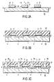
- FIG. 19A for example, in the case of the ferroelectric RAM of the conventional structure where neither the COP structure nor the series connected TC unit type ferroelectric RAM architecture is adopted, not only a contact region 103 to be connected to an upper electrode 101 or a lower electrode 102 of the capacitor, but also a connecting wiring 105 to be connected to a diffusion layer 104 are necessary. Moreover, a predetermined space is required between a contact hole of the contact region 103 and the connecting wiring 105 , and at the same time, a large number of connecting wirings 105 and hence a large number of spaces for the connecting wirings 105 are required to be provided, so that the area required to be allocated to the layout of each cell would become large inevitably. For example, when the minimum dimension to be employed in designing the ferroelectric RAM is defined as F, the cell size of FIG. 19A would become 8F 2 .
- FIG. 19 B One of the methods which are capable of minimizing the area required for the layout of each cell is the aforementioned series connected TC unit type ferroelectric RAM architecture, the structure of which is illustrated in FIG. 19 B.
- This cell is formed to have a size 6F 2 wherein the upper electrode 111 of the capacitor is commonly used by a couple of neighboring cells, and two lower electrodes 112 of a couple of neighboring cells are provided to the common upper electrode 111 .
- Each of these electrodes 111 and 112 is connected via a contact 113 with a diffusion layer 114 . Further, this diffusion layer 114 is also commonly used by a couple of neighboring transistors Tr.
- FIG. 19C a series connected TC unit type ferroelectric RAM architecture having a structure as shown in FIG. 19C has been proposed.
- This ferroelectric RAM architecture having such a structure can be represented by an equivalent circuit as shown in FIG. 20 .
- diffusion regions 124 to be employed respectively as a source and a drain with a gate electrode G of one memory cell transistor Tr being interposed therebetween are connected via contact plugs 123 with the upper electrode 121 and lower electrode 122 of a capacitor Cf, respectively.
- Each of these diffusion regions 124 is commonly used as the source and drain of transistors of the neighboring cells, thereby constituting an architecture connected with each other in the form of a chain.
- the COP structure is applied to both upper and lower electrodes 121 and 122 , thereby suggesting the possibility of obtaining, under ideal conditions, a most miniaturized cell size of 4F 2 as shown in FIG. 19 C.
- This structure shown in FIG. 19C accompanies with many difficulties before it can be actually realized.
- tungsten which is vulnerable to oxidation is employed for the fabrication of contact plug 123
- the upper limit of the process temperature is determined depending on the barrier properties of the barrier film. Therefore, it is very difficult at present to combine the structure of FIG. 19C with the employment of a barrier film of SBT whose film-forming temperature is 700° C. or more.
- both upper and lower electrodes are constituted by the COP structure, i.e. a structure where the electrodes are taken up from the beneath or underside of the ferroelectric capacitor Cf. Therefore, both upper and lower electrodes 121 and 122 necessitate the provision of a conductive barrier film.
- an object of this invention is to provide a ferroelectric memory which enables to realize the miniaturization of the cell, which can be manufactured by a simple manufacturing process, and which is stable in characteristics.
- Another object of this invention is to provide a method of manufacturing such a ferroelectric memory as described above.
- This invention provides a ferroelectric memory wherein a horizontal type ferroelectric capacitor is disposed immediately above a memory cell transistor, in which a pair of capacitor electrodes having a ferroelectric layer sandwiched therebetween are arranged horizontally in a direction along with a surface of a semiconductor substrate.
- this invention provides a ferroelectric memory which is capable of realizing an extremely miniaturized cell size without necessitating a conductive barrier film which has been deemed as being indispensable in the prior art.
- This invention also provides a method of manufacturing a ferroelectric memory having these desired features.
- a ferroelectric capacitor is horizontally disposed along with the surface of the semiconductor substrate, so that the pair of electrodes, arranged in the horizontal direction to face to each other, of the ferroelectric capacitor can be simultaneously formed in a manufacturing step, thereby making it possible to reduce the number of manufacturing steps and at the same time, to homogenize the properties of the electrodes.
- the lower and upper electrodes of the ferroelectric capacitor are stacked vertically in a direction normal to the surface of the semiconductor substrate, the lower and upper electrodes should be formed in different steps.
- an insulating barrier film is employed as a barrier film to be formed on a contact plug.
- a restoring annealing is performed, which is followed by a step of forming a wiring layer connected with neighboring cells and also with contact plugs formed on a diffusion region.
- ferroelectric memory according to one aspect of this invention is featured in that it comprises;
- ferroelectric capacitor horizontally disposed over the MOS transistor in a channel length direction of the MOS transistor
- metallic wirings respectively formed on and connected with contact plugs which are connected with the source/drain regions, the metallic wirings respectively having a sidewall which is contacted with the electrodes of the ferroelectric capacitor.
- the present invention also provides a method of manufacturing a ferroelectric memory, which comprises;
- contact plugs in contact regions of the insulating film, the contacting regions corresponding with source/drain and gate of the MOS transistors;
- a pair of electrodes of the ferroelectric capacitor can be simultaneously formed, thereby making it possible to reduce the number of manufacturing steps and also to expand the facing area of the ferroelectric capacitor not only in the horizontal direction but also in the vertical direction of the semiconductor substrate, and hence the chip size can be miniaturized inversely proportion to the magnitude of this expansion.
- an insulating barrier film is formed between a memory cell transistor and a ferroelectric capacitor according to one embodiment of this invention, the process margin or tolerance can be increased, and at the same time, it becomes possible to carry out a sufficient heat treatment for restoring any damage to the ferroelectric capacitor which would be inevitably caused during the manufacture of a ferroelectric memory, thus making it possible to manufacture a ferroelectric memory having excellent properties.
- FIG. 1A shows a top plan view of a ferroelectric memory illustrating one embodiment of this invention
- FIGS. 1B and 1C show respectively a cross-sectional view of the ferroelectric memory shown in FIG. 1A;
- FIGS. 2A to 2 C show respectively a cross-sectional view for illustrating the manufacturing method of the ferroelectric memory shown in FIGS. 1A to 1 C;
- FIGS. 3A to 3 C show respectively a cross-sectional view for illustrating the manufacturing method of the ferroelectric memory shown in FIGS. 1A to 1 C;
- FIGS. 4A to 4 C show respectively a cross-sectional view for illustrating the manufacturing method of the ferroelectric memory shown in FIGS. 1A to 1 C;
- FIGS. 5A and 5B show respectively a cross-sectional view for illustrating the manufacturing method of the ferroelectric memory shown in FIGS. 1A to 1 C;
- FIG. 6A shows a top plan view of a ferroelectric memory illustrating a second embodiment of this invention
- FIGS. 6B and 6C show respectively a cross-sectional view of the ferroelectric memory shown in FIG. 6A;
- FIGS. 7A to 7 C show respectively a cross-sectional view for illustrating the manufacturing method of the ferroelectric memory shown in FIGS. 6A to 6 C;
- FIG. 8A shows a top plan view of a ferroelectric memory illustrating a third embodiment of this invention.
- FIGS. 8B and 8C show respectively a cross-sectional view of the ferroelectric memory shown in FIG. 8A;
- FIGS. 9A to 9 C show respectively a cross-sectional view for illustrating the manufacturing method of the ferroelectric memory shown in FIGS. 8A to 8 C;
- FIGS. 10A to 10 C show respectively a cross-sectional view for illustrating the manufacturing method of the ferroelectric memory shown in FIGS. 8A to 8 C;
- FIGS. 11A to 11 C show respectively a cross-sectional view for illustrating the manufacturing method of the ferroelectric memory shown in FIGS. 8A to 8 C;
- FIG. 12A shows a top plan view of a ferroelectric memory illustrating a fourth embodiment of this invention
- FIGS. 12B and 12C show respectively a cross-sectional view of the ferroelectric memory shown in FIG. 12A;
- FIGS. 13A to 13 C show respectively a cross-sectional view for illustrating the manufacturing method of the ferroelectric memory shown in FIGS. 12A to 12 C;
- FIGS. 14A to 14 C show respectively a cross-sectional view for illustrating the manufacturing method of the ferroelectric memory shown in FIGS. 12A to 12 C;
- FIG. 15A shows a top plan view of a ferroelectric memory illustrating a fifth embodiment of this invention.
- FIGS. 15B and 15C show respectively a cross-sectional view of the ferroelectric memory shown in FIG. 15A;
- FIGS. 16A to 16 C show respectively a cross-sectional view for illustrating the manufacturing method of the ferroelectric memory shown in FIGS. 6A to 6 C or in FIGS. 12A to 12 C;
- FIG. 17 shows a cross-sectional view for illustrating the manufacturing method of the ferroelectric memory shown in FIGS. 6A to 6 C or in FIGS. 12A to 12 C;
- FIG. 18 shows a top plan view of a ferroelectric memory illustrating a sixth embodiment of this invention.
- FIGS. 19A to 19 C show respectively a cross-sectional view for illustrating various examples of ferroelectric memory according to the prior art.
- FIG. 20 illustrates the structure of the circuit of a series connected TC unit type ferroelectric RAM according to the prior art.
- FIGS. 1A to 1 C show the structure of a series connected TC unit type ferroelectric RAM representing a first embodiment of this invention. Specifically, FIG. 1A shows a plan view; FIG. 1B is a cross-sectional view taken along the line A-B of FIG. 1A; and FIG. 1C is a cross-sectional view taken along the line C-D of FIG. 1 A.
- a plurality of buried element isolation regions 2 are formed in a stripe pattern on the surface of a semiconductor substrate 30 , and a plurality of element regions 1 are defined between these element isolation regions 2 .
- a diffusion layer 4 is formed in a self-alignment manner relative to the gate electrode 3 of each transistor Tr.
- the gate electrode 3 is formed on the surface of a gate insulating film 21 constituting a first insulating film, thereby constructing a plurality of MOS transistors Tr of one conductivity type.
- the MOS transistors Tr are covered by a second insulating film 22 which has a surface smoothed by means of a CMP method, for example.
- a contact plug 8 is buried in the second insulating film 22 and contacted with the diffusion region or layer 4 .
- another contact plugs are buried as gate contacts 8 G for the gate electrode 3 at a region over the element isolation regions 2 .
- These contact plugs can be formed using polycrystalline silicon doped with a high concentration of impurities or using tungsten (W).
- a ferroelectric capacitor Cf comprising a successive array of a ferroelectric capacitor electrode 9 a, a ferroelectric film 10 constituting a third insulating film, and another ferroelectric capacitor electrode 9 b is formed immediately over each of the MOS transistors Tr with the second insulating film 22 being interposed therebetween.
- the ferroelectric capacitor Cf is horizontally disposed extending in the gate length direction of the gate of the transistor Tr.
- the ferroelectric capacitor electrodes 9 a and 9 b and the ferroelectric film 10 are arranged in a lateral direction along with a surface of the semiconductor substrate 30 .
- a fourth insulating film 11 is formed on the top of the ferroelectric capacitor Cf.
- a metallic wiring 14 is disposed on the top of the contact plug 8 which is contacted with the diffusion layer 4 of the transistor Tr.
- the both sides of the metallic wiring 14 are electrically connected with the right and left electrodes 9 a and 9 b of a pair of neighboring ferroelectric capacitors Cf neighboring the metallic wiring 14 .
- an insulating film 13 is formed on the tops of the ferroelectric capacitor Cf and of the metallic wiring 14 .
- a bit line BL is laterally formed along the element region 1 .
- a passivation film is formed on the top of the bit line BL, thereby accomplishing a ferroelectric memory.
- the distance between a pair of contact plugs 8 in the direction along the element region 1 is 2F as shown in FIG. 1A, and hence, the dimension in the direction crossing the element region 1 is also 2F. Therefore, the area of a single memory cell would become 4F 2 , thereby achieving an ultimate miniaturization.
- the horizontal ferroelectric capacitor Cf is formed between a pair of neighboring metallic wirings 14 .
- the intervals between a pair of neighboring metallic wirings 14 is 1.5F for instance, as shown in FIG. 1B, so that a pair of capacitor electrodes 9 a and 9 b, and the ferroelectric film 10 are formed within this interval.
- the dimension of this ferroelectric film 10 in thickness-wise direction of the substrate 30 is 2F or more, this dimension can be optionally determined depending on the capacity designed of the ferroelectric capacitor Cf.
- both of the capacitor electrodes 9 a and 9 b of the ferroelectric capacitor Cf can be concurrently worked in one wiring layer in contrast to the prior art wherein capacitor electrodes of a capacitor should have been separately worked in the thickness direction of the semiconductor substrate. Therefore, it is possible according to this embodiment to reduce the number of manufacturing steps and also to inhibit the non-uniformity of the characteristics of these capacitor electrodes 9 a and 9 b.
- FIGS. 1A to IC the manufacturing process of the ferroelectric memory having a structure as shown in FIGS. 1A to IC will be explained with reference to FIGS. 2A to 2 C, FIGS. 3A to 3 C, FIGS. 4A to 4 C, and FIGS. 5A and 5B.
- FIGS. 2A to 2 C the manufacturing process of the ferroelectric memory having a structure as shown in FIGS. 1A to IC will be explained with reference to FIGS. 2A to 2 C, FIGS. 3A to 3 C, FIGS. 4A to 4 C, and FIGS. 5A and 5B.
- the following explanations are made with reference to the cross-sectional view taken along the line A-B of FIG. 1A, or the cross-sectional view to be obtained by cutting the element region 1 in longitudinal direction thereof.
- FIG. 2A shows a state wherein a gate 3 is formed via a gate oxide film 21 on the surface of the element region 1 , after the element region 1 has been formed between a pair of element isolation regions 2 which have been formed on the surface of n-type semiconductor substrate 30 as shown in FIGS. 1A and 1C.
- the distance between a pair of neighboring gates 3 in this case is 1.5F for instance, and the gate length of the gate 3 is set to F.
- the gate width it is formed slightly narrower than the width of the element region 1 as shown in FIG. 1 A.
- a p-type diffusion layers 4 are formed in a self-alignment manner with the gate 3 being employed as a mask, after which an interlayer insulating film 22 is deposited thereon, the surface of the interlayer insulating film 22 thus deposited being subsequently flattened by means of a CMP method.
- a resist is coated on the surface of the interlayer insulating film 22 and then subjected to an exposure treatment which is followed by a developing treatment, thereby forming a resist mask. Then, by making use of this resist mask, a contact hole 8 a extending to the diffusion layer 4 is formed at an intermediate portion of the neighboring gates 3 . Further, tungsten (W) as a material for the contact plug is deposited inside the contact hole 8 a. The tungsten layer thus formed and the interlayer insulating film 22 are then shaped into a desired configuration by means of a CMP method to thereby form a contact plug 8 . By the way, it is possible to employ, as a material for the contact plug, a doped polycrystalline silicon other than tungsten.
- an insulating film 14 i is deposited all over the surface of the product of FIG. 2 C.
- the insulating film 14 i is selectively etched away so as to leave the insulating film 14 i partially only on the top portion of the contact plug 8 .
- the width of the insulating film 14 i which has been left as shown in FIG. 3B is formed larger than each contact plug 8 with a view to take into consideration any misalignment of the mask to be employed on the occasion of etching. Ideally however, it is preferable to form the left insulating film 14 i at the same width as that of the contact plug 8 .
- an electrode film made of prutinum (Pt), for instance, is entirely deposited by means of a sputtering method, which is followed by a heat treatment and then by a flattening step by making use of a CMP method, thereby forming an electrode film 9 between each pair of the left insulating films 14 i.
- the electrode film may be deposited after the formation of a stopper film on the top portion of the left insulating films 14 i so as to prevent the left insulating films 14 i from being badly affected by the material to be employed for the electrode film 9 .
- a cut region 10 a for forming the ferroelectric film 10 shown in FIG. 1A is formed at a central portion of the electrode film 9 by means of etching.
- a resist mask it is important to form the opening of the resist mask corresponding to this ferroelectric film-forming region 10 a in such a manner that the opening extends over the region of the electrodes 9 a and 9 b.
- the ferroelectric capacitor electrodes 9 a and 9 b can be reliably insulated by the ferroelectric film 10 to be subsequently deposited between the electrodes 9 a and 9 b.
- the ferroelectric material is deposited all over the surface including the ferroelectric film-forming region 10 a by means of a spin-coating method which enables to obtain a homogenous film followed by a CMP method to leave the ferroelectric material in the forming region 10 a to form a ferroelectric film 10 .
- an insulating film 11 is entirely deposited. Thereafter, the surface of the insulating film 11 is flattened by means of the CMP method, thereby obtaining a ferroelectric capacitor Cf.
- the left insulating films 14 i that has been formed in advance is etched away together with corresponding portions of the insulating film 11 to form an opening 14 a to thereby allow the surface of the contact plug 8 to expose from the bottom of the opening 14 a and the side surfaces of the capacitor electrodes 9 a and 9 b to expose to the opening 14 a.
- the resultant structure is subjected to an oxygen annealing at a temperature of 600° C. to 700° C. so as to sufficiently restore or recover any damage to the ferroelectric film 10 that may be brought about up to this step. If both of the insulating films 11 and 14 i are formed of the same insulating material, this etching can be accomplished using only one step.
- a conductive material is entirely deposited, and the surface thereof is flattened by making use of a CMP method so as to make it flush with the surface of the insulating film 11 until metallic wirings 14 are left in the openings 14 a. It is possible in this case to further apply a heat treatment for effecting the reflow of the surface. In this way, the metallic wiring 14 can be formed only at the opening portions 14 a, and at the same time, the connection thereof with both electrodes 9 a and 9 b of the ferroelectric capacitor Cf as well as the connection thereof with the contact plugs 8 can be concurrently achieved.
- an insulating film 13 is entirely deposited, and the surface thereof is flattened by making use of a CMP method, after which a bit line BL is formed laterally on the resultant surface.
- an ordinary passivation film is entirely formed on the resultant surface, thereby finishing the manufacturing process of the ferroelectric memory. By undergoing these steps, it is possible to obtain a miniaturized series connected TC unit type ferroelectric RAM having a horizontal ferroelectric capacitor Cf.
- a high-temperature annealing for restoring a damage to the ferroelectric film 10 is applied under the condition where the contact plug 8 is being exposed as shown in FIG. 4 C.
- the surface of the contact plug 8 exposed in this manner is vulnerable to oxidation, so that there is a possibility that a contact failure may be caused to occur between the contact plug 8 and the metallic wiring 14 to be subsequently formed thereon.
- This second embodiment differs from the aforementioned first embodiment in the respect that as shown in FIGS. 6C and 6C, a laminate film consisting of a nitride film 6 and an oxide film 7 is interposed as an oxidative diffusion barrier film between an interlayer insulating film 22 and a ferroelectric capacitor Cf. Due to the existence of these oxidative diffusion barrier films 6 and 7 , it becomes possible to completely inhibit the oxidation of the contact plug 8 as well as the diffusion of impurities into the transistor region 4 during the step of forming the ferroelectric capacitor Cf.
- the thickness of the nitride film 6 and the oxide film 7 is set respectively to 150 nm, it is possible to secure a sufficient barrier property even in a heat treatment in a furnace of 700° C.
- an oxynitride film containing a sufficient degree of nitrogen in place of these oxidative diffusion barrier films 6 and 7 .
- FIGS. 6A to 6 C other constituents are all the same as those of the embodiment illustrated in FIGS. 1A to 1 C, so that these same constituents will be represented by the same reference numbers, thereby omitting a further explanation thereof.
- FIGS. 6A to 6 C will be explained with reference to FIGS. 7A to 7 C wherein only the manufacturing steps which differ from those of the first embodiment shown in FIGS. 1A to 1 C will be explained to thereby avoid the duplication and complication of explanation.
- an insulating film 14 i is formed on the surface of this oxide film 7 in the same manner as shown in FIG. 3 A. Thereafter, the same manufacturing process as illustrated as that of the first embodiment until the step of FIG. 4C is finished is repeated. In the same manner as explained in FIG. 4C, the etching is temporarily suspended under the condition where the insulating films 11 and 14 i are etched away.
- FIG. 7 B This condition is illustrated in FIG. 7 B. Namely, when the oxide film 7 is exposed after the removal of the insulating films 11 and 14 i by means of etching, the etching is suspended, wherein the surface of the contact plug 8 is covered by the films 6 and 7 . Thereafter, an oxygen annealing is performed at a temperature of about 600° C. to 700° C. to thereby sufficiently restore a damage to the ferroelectric film 10 that has been brought about by the working performed up to this moment.
- these oxidative diffusion barrier films 6 and 7 are then removed as shown in FIG. 7C, thereby allowing the contact plug 8 to expose. Thereafter, in the same manner as shown in FIGS. 5A and 5B, a metallic wiring 14 is formed, and a bit line BL is formed via an insulating film 13 .
- the annealing for restoring or recovering the ferroelectric capacitor Cf can be performed in an oxygen atmosphere at a sufficiently high temperature, thereby making it form an electrode film 9 in each space between the insulating films 14 i.
- a conductive material may be deposited after the formation of a stopper film on the top portion of the insulating films 14 i so as to prevent the insulating films 14 i from being badly affected by the material to be employed for the electrode material 9 .
- an opening region 10 a for forming the ferroelectric film 10 is formed at a central portion of the electrode film 9 by means of etching.
- a resist mask it is important to form an opening for this ferroelectric film-forming opening region 10 a in such a manner that the opening defined by the resist mask extends over the edges of the capacitor electrodes 9 a and 9 b.
- the ferroelectric capacitor electrodes 9 a and 9 b can be reliably insulated by the ferroelectric film 10 to be subsequently deposited.
- a ferroelectric material for the ferroelectric film 10 is deposited all over the surface including the ferroelectric film-forming region 11 a and a CMP method is performed until the surfaces of the capacitor electrodes 9 a and 9 b are exposed, and then an insulating film 11 is entirely possible to obtain a ferroelectric memory having excellent properties.
- FIGS. 8A to 8 C illustrate a third embodiment of this invention. This embodiment differs from the second embodiment shown in FIGS. 6A to 6 C in that the metallic wiring 14 to be contacted with the contact plug 8 is tapered in such a manner that an upper portion thereof is wider and a lower portion thereof contacted with the contact plug 8 is almost identical in cross-sectional area with that of the contact plug 8 .
- FIG. 9A is identical with the step shown in FIG. 7 A.
- the step shown in FIG. 9B corresponds to the step shown in FIG. 7B except that the barrier films 6 and 7 are formed therein, but differs from the step of FIG. 7B in the respect that according to FIG. 9B, an insulating film mask 14 i having almost the same width as that of the contact plug 8 is formed therein.
- an electrode film such as a plutinum film is deposited all over the surface including the insulating film mask 14 i.
- the resultant electrode film is then heat-treated and flattened by means of a CMP method to thereby deposited.
- the surface of the insulating film 11 is flattened by means of the CMP method, thereby obtaining a ferroelectric capacitor Cf having the ferroelectric film 10 which is sandwiched between a pair of electrodes 9 a and 9 b.
- the insulating films 14 i and the side walls of the capacitor electrodes 9 a and 9 b that have been formed in advance are partially etched away together with the insulating film 11 to form an opening 14 a having a tapered configuration or a cone-shaped configuration, thereby allowing the surfaces of the nitride film 7 as well as the capacitor electrodes 9 a and 9 b to expose from the bottom and side wall of the opening 14 a.
- the resultant structure is subjected to an oxygen annealing at a temperature of 600° C. to 700° C. so as to sufficiently restore any damage to the ferroelectric film 10 that may be brought about up to this step. If both of the insulating films 11 and 14 i are formed of the same insulating material, this etching can be accomplished using only one step.
- the oxidative diffusion barrier film structure including the nitride film 7 and the oxide film 6 is etched away to thereby allow the surface of the contact plug 8 to expose.
- a conductive material for the metallic wiring 14 is entirely deposited, and the surface thereof is flattened by making use of a CMP method so as to make the resultant metallic wiring flush with the surface of the insulating film 11 . It is possible in this case to further apply a heat treatment for effecting the reflow of the surface.
- the metallic wiring 14 can be left only at the opening portions 14 a, and at the same time, the connection thereof with both electrodes 9 a and 9 b of the ferroelectric capacitor Cf as well as the connection thereof with the contact plugs 8 can be concurrently achieved.
- an insulating film 13 is entirely deposited, and the surface thereof is flattened by making use of a CMP method, after which a bit line BL is formed on the resultant surface.
- an ordinary passivation film is entirely formed on the resultant surface, thereby finishing the manufacturing process of the ferroelectric memory.
- a top portion of each of the prutinum electrodes 9 a and 9 b of the ferroelectric capacitor Cf disposed on the sidewall of the opening 14 a may be erased away on the occasion of etching the barrier films 6 and 7 .
- the damage to the ferroelectric capacitor Cf which may be caused on this occasion can be minimized by suspending the etching immediately before the barrier films 6 and 7 , and then, by the subsequent high-temperature annealing.
- the ferroelectric film 10 is constructed in such a manner that side portions of the ferroelectric film 10 facing the element isolating regions 2 is formed not in a flush state relative to the corresponding portions of the right and left electrodes 9 a and 9 b, but is positively extended over the right and left electrodes 9 a and 9 b in the direction of the element isolating regions 2 , thereby forming an off-set structure.
- these right and left electrodes 9 a and 9 b can be prevented from suffering from short-circuit, thereby making it possible to improve the manufacturing yield.
- FIGS. 13A to 13 C illustrates one example where the electrodes 9 a and 9 b of the ferroelectric capacitor Cf is crystallized on the plane of the nitride film 7 .
- FIGS. 13A to 13 C correspond to the steps shown in FIGS. 7A to 7 C or to the steps shown in FIGS. 9A to 9 C, but differ from these latter steps in the respect that contact barrier films 6 and 7 are formed at first in place of the insulating film 14 i, and then, a capacitor electrode film 9 is formed by means of a sputtering method or a coating method as shown in FIG. 13 B.
- the capacitor electrode film 9 which is located in the region for forming the ferroelectric film 10 is etched away to form an opening 10 a.
- the ferroelectric film 10 is filled only in the opening 10 a, and then, an insulating film 11 is deposited thereon. Then, as shown in FIG. 14B, the capacitor electrode film 9 and the insulating film 11 , both disposed over the contact plug 8 , are etched away. In this case also, the etching is temporarily suspended at the portions of contact barrier films 6 and 7 .
- the annealing for restoring any damage induced by the working is performed for about one hour at a temperature of 700° C.
- These barrier films 6 and 7 are then entirely back-etched to thereby allow the contact plug 8 to expose, and then, a metallic wiring 14 is filled and buried therein to obtain a structure as shown in FIG. 14 C.
- the material for this metallic wiring 14 it is preferable to employ a film containing aluminum (Al) or copper (Cu) as a main component and combined with a liner material including titanium (Ti) or niobium (Nb).
- the procedures to be performed thereafter are the same as those of the embodiment shown in FIGS. 8A to 8 C.
- the structure of the embodiment shown in FIGS. 15A to 15 C is almost the same as the embodiment shown in FIGS. 6A to 6 C, but differs from that of the embodiment shown in FIGS. 6A to 6 C in the respect that conductive oxide films 15 a and 15 b are formed on the sides of the ferroelectric film 10 as shown in FIGS. 15A and 15B.
- the conductive oxide films it is possible to employ iridium oxide (IrO 2 ), rutenium oxide (RuO 2 ) or strontium oxide (SrO).
- electrodes 9 are formed at first, and an opening is formed at a central portion of each electrode 9 to leave a pair of electrodes 9 a and 9 b of the ferroelectric capacitor Cf. Thereafter, a conductive oxide film is deposited all over the surface including the aforementioned opening formed between the electrodes 9 a and 9 b. Then, an opening is formed at a central portion between the electrodes 9 a and 9 b of each capacitor element by means of a CMP method or an RIE method in such a manner that the sidewall film portions 15 a and 15 b formed of the conductive oxide films are left on both sidewalls of the opening. Then, a ferroelectric material for the ferroelectric film 10 is filled and buried in the opening to form the ferroelectric film 10 . Other constituents are the same as those of the embodiment illustrated in FIGS. 6A to 6 C.
- a conductive oxide films 15 a and 15 b are disposed on the sidewall of the ferroelectric film 10 between the respective capacitor electrodes 9 a and 9 b, the fatigue characteristics of the ferroelectric capacitor Cf, i.e. the allowable number of data rewriting can be greatly improved, thereby making it possible to provide a ferroelectric RAM which is free from changes in data memory characteristics in a long-term use and is excellent in reliability.
- FIGS. 16A to 16 C and FIG. 17 illustrate a manufacturing process according to another embodiment of this invention, wherein the step shown in FIG. 16A is the same as that of FIG. 13 A. Thereafter, as shown in FIG. 16B, an insulation film is formed and then, etched so as to selectively leave a dummy film 10 d at the regions for forming the ferroelectric film 10 . Subsequently, the deposition of platinum electrodes 9 and the CMP treatment are performed so as to accomplish the working of the platinum electrodes.
- the dummy film 10 d is replaced by the ferroelectric film 10 .
- the dummy film 10 d is etched away to form an opening between the neighboring electrodes 9 , into which the ferroelectric film 10 is filled and then, the resultant surface is flattened as required by the CMP method, for example.
- This step corresponds to the step shown in FIG. 14 A.
- the subsequent steps to be followed are the same as those shown in FIGS. 14B and 14C.
- the sidewall of the opening 10 a is caused to become tapered in order to secure a sufficient area at the bottom of the opening 10 a, thereby inevitably increasing the area at the edge portion of the opening 10 a.
- the dummy film 10 d which can be easily worked is employed, it becomes possible to form an opening having a normally vertical sidewall. Namely, since the opening 10 a is free from a tapered sidewall and hence free from a pattern conversion difference, it is possible to obtain a further miniaturized cell.
- the step of FIG. 17 may be followed, as shown in FIG. 18, by a step in which a composite barrier film 16 having the same structure as that of barrier films 6 and 7 is formed prior to the deposition of this insulating film 11 , thereby making it possible to minimize the thinning of film of the electrode 9 in the etching step of the barrier films 6 and 7 which corresponds to the step of FIG. 14B where the etching is performed down to reach the contact plug 8 .
- the damage caused on the occasion of depositing the ferroelectric film 10 can be recovered in the so-called recovery/annealing step, and additionally, the resistivity to damage in the subsequent annealing step in a hydrogen gas atmosphere can be improved, thereby extremely improving the capacitor characteristics of the ferroelectric memory.
- LDD type structure As a structure for the diffusion layer 4 of the memory cell transistor.
- a silicide layer may be formed on the surface of the diffusion layer 4 acting as a source or a drain or on the gate 3 . If a silicide is to be employed, it is especially desirable to employ the diffusion barrier films 6 and 7 in view of the problems of heat resistance and oxidation resistance. Further, if the contact plug 8 is to be formed by depositing a polycrystalline silicon, it is necessary to take into consideration the concentration of impurities so as to make it possible to obtain a sufficiently low contact resistance.
- a ferroelectric capacitor is horizontally disposed instead of disposing it vertical as in the conventional structure, a pair of electrodes, facing to each other and corresponding to the upper and lower electrodes, of a ferroelectric capacitor which have been conventionally formed separately in the prior art can be simultaneously formed in a first or second wiring layer, for example, thereby making it possible to reduce the number of manufacturing steps.
- a COT (Capacitor Over Transistor) structure is adopted in this invention instead of the COP structure, it is now possible to miniaturize the size of cell to an ultimate size of 4F 2 , thereby making it possible to obtain a ferroelectric capacitor exhibiting excellent properties and to further miniaturize the ferroelectric capacitor.
- an insulating oxidative diffusion barrier film such as an silicon nitride (SiN) film (a laminate structure of oxide film/nitride film) up to the step of forming a contact hole for exposing the contact plug
- SiN silicon nitride
- this invention can be applied to the SBT which is indispensable for obtaining a film of high temperature resistance and exhibiting excellent properties.
- the manufacturing process according to this invention it is possible to make uniform the structure of films including that of memory cell and those of other components located other than the memory cell in making contact with the contact plug, thereby simplifying the process. Further, a pair of facing electrodes of the ferroelectric capacitor can be simultaneously formed, and hence, even if platinum is employed as an electrode material, the time to etch the platinum can be shortened, thereby making it possible to minimize any damage to the ferroelectric capacitor, which may be induced during the working of the ferroelectric capacitor.
- the capacitor electrodes 9 a, 9 b may be formed at least of a single substance film of a material selected from a group consisting of Pt, Ir, IrO 2 , Ru, RuO 2 , and SrO 2 ; and of a multi-layered film comprising two or more materials of the single substrate film.
Landscapes
- Semiconductor Memories (AREA)
Applications Claiming Priority (2)
| Application Number | Priority Date | Filing Date | Title |
|---|---|---|---|
| JP2000087402A JP3828332B2 (ja) | 2000-03-27 | 2000-03-27 | 強誘電体メモリ |
| JP2000-087402 | 2000-03-27 |
Publications (2)
| Publication Number | Publication Date |
|---|---|
| US20010048624A1 US20010048624A1 (en) | 2001-12-06 |
| US6504198B2 true US6504198B2 (en) | 2003-01-07 |
Family
ID=18603416
Family Applications (1)
| Application Number | Title | Priority Date | Filing Date |
|---|---|---|---|
| US09/816,478 Expired - Fee Related US6504198B2 (en) | 2000-03-27 | 2001-03-26 | Horizontal type ferroelectric memory and manufacturing method of the same |
Country Status (2)
| Country | Link |
|---|---|
| US (1) | US6504198B2 (enExample) |
| JP (1) | JP3828332B2 (enExample) |
Cited By (5)
| Publication number | Priority date | Publication date | Assignee | Title |
|---|---|---|---|---|
| US20030129796A1 (en) * | 2001-06-29 | 2003-07-10 | Rainer Bruchhaus | Method for fabricating a semiconductor memory device |
| US20030228726A1 (en) * | 2002-06-06 | 2003-12-11 | Hasan Nejad | Magnetoresistive memory device assemblies |
| US20050248975A1 (en) * | 2004-05-07 | 2005-11-10 | Kabushiki Kaisha Toshiba | Semiconductor storage device and its manufacturing method |
| US20060284224A1 (en) * | 2005-06-20 | 2006-12-21 | Susumu Shuto | Ferroelectric memory device and method of manufacturing the same |
| US20080079046A1 (en) * | 2006-09-28 | 2008-04-03 | Kabushiki Kaisha Toshiba | Semiconductor apparatus and method for manufacturing the same |
Families Citing this family (9)
| Publication number | Priority date | Publication date | Assignee | Title |
|---|---|---|---|---|
| US6795329B2 (en) * | 2002-06-20 | 2004-09-21 | Infineon Technologies Aktiengesellschaft | Memory integrated circuit |
| US20040163233A1 (en) * | 2003-02-26 | 2004-08-26 | Stefan Gernhardt | Methods of forming electrical connections within ferroelectric devices |
| US7473596B2 (en) * | 2003-12-19 | 2009-01-06 | Micron Technology, Inc. | Methods of forming memory cells |
| JP2006269764A (ja) * | 2005-03-24 | 2006-10-05 | Toshiba Corp | 強誘電体記憶装置および製造方法 |
| US7320934B2 (en) | 2005-06-20 | 2008-01-22 | Infineon Technologies Ag | Method of forming a contact in a flash memory device |
| US8803245B2 (en) * | 2008-06-30 | 2014-08-12 | Mcafee, Inc. | Method of forming stacked trench contacts and structures formed thereby |
| JP2010080628A (ja) * | 2008-09-25 | 2010-04-08 | Toshiba Corp | 半導体記憶装置及びその製造方法 |
| US10217794B2 (en) | 2017-05-24 | 2019-02-26 | Globalfoundries Singapore Pte. Ltd. | Integrated circuits with vertical capacitors and methods for producing the same |
| JP7173909B2 (ja) * | 2019-03-20 | 2022-11-16 | キオクシア株式会社 | 半導体記憶装置 |
Citations (5)
| Publication number | Priority date | Publication date | Assignee | Title |
|---|---|---|---|---|
| US5576928A (en) * | 1994-08-01 | 1996-11-19 | Texas Instruments Incorporated | High-dielectric-constant material electrodes comprising thin platinum layers |
| US5903492A (en) | 1996-06-10 | 1999-05-11 | Kabushiki Kaisha Toshiba | Semiconductor memory device and various systems mounting them |
| US6033919A (en) * | 1996-10-25 | 2000-03-07 | Texas Instruments Incorporated | Method of forming sidewall capacitance structure |
| US6094370A (en) | 1996-06-10 | 2000-07-25 | Kabushiki Kaisha Toshiba | Semiconductor memory device and various systems mounting them |
| US6124164A (en) * | 1998-09-17 | 2000-09-26 | Micron Technology, Inc. | Method of making integrated capacitor incorporating high K dielectric |
-
2000
- 2000-03-27 JP JP2000087402A patent/JP3828332B2/ja not_active Expired - Fee Related
-
2001
- 2001-03-26 US US09/816,478 patent/US6504198B2/en not_active Expired - Fee Related
Patent Citations (5)
| Publication number | Priority date | Publication date | Assignee | Title |
|---|---|---|---|---|
| US5576928A (en) * | 1994-08-01 | 1996-11-19 | Texas Instruments Incorporated | High-dielectric-constant material electrodes comprising thin platinum layers |
| US5903492A (en) | 1996-06-10 | 1999-05-11 | Kabushiki Kaisha Toshiba | Semiconductor memory device and various systems mounting them |
| US6094370A (en) | 1996-06-10 | 2000-07-25 | Kabushiki Kaisha Toshiba | Semiconductor memory device and various systems mounting them |
| US6033919A (en) * | 1996-10-25 | 2000-03-07 | Texas Instruments Incorporated | Method of forming sidewall capacitance structure |
| US6124164A (en) * | 1998-09-17 | 2000-09-26 | Micron Technology, Inc. | Method of making integrated capacitor incorporating high K dielectric |
Cited By (14)
| Publication number | Priority date | Publication date | Assignee | Title |
|---|---|---|---|---|
| US6858492B2 (en) * | 2001-06-29 | 2005-02-22 | Infineon Technologies Ag | Method for fabricating a semiconductor memory device |
| US20030129796A1 (en) * | 2001-06-29 | 2003-07-10 | Rainer Bruchhaus | Method for fabricating a semiconductor memory device |
| US20060076635A1 (en) * | 2002-06-06 | 2006-04-13 | Hasan Nejad | Magnetoresistive memory device assemblies, and methods of forming magnetoresistive memory device assemblies |
| US6781174B2 (en) * | 2002-06-06 | 2004-08-24 | Micron Technology, Inc. | Magnetoresistive memory device assemblies |
| US20050040453A1 (en) * | 2002-06-06 | 2005-02-24 | Hasan Nejad | Magnetoresistive memory device assemblies |
| US20030228726A1 (en) * | 2002-06-06 | 2003-12-11 | Hasan Nejad | Magnetoresistive memory device assemblies |
| US7038286B2 (en) | 2002-06-06 | 2006-05-02 | Micron Technology, Inc. | Magnetoresistive memory device assemblies |
| US7279762B2 (en) | 2002-06-06 | 2007-10-09 | Micron Technology, Inc. | Magnetoresistive memory device assemblies, and methods of forming magnetoresistive memory device assemblies |
| US20050248975A1 (en) * | 2004-05-07 | 2005-11-10 | Kabushiki Kaisha Toshiba | Semiconductor storage device and its manufacturing method |
| US20060284224A1 (en) * | 2005-06-20 | 2006-12-21 | Susumu Shuto | Ferroelectric memory device and method of manufacturing the same |
| US7535745B2 (en) * | 2005-06-20 | 2009-05-19 | Kabushiki Kaisha Toshiba | Ferroelectric memory device and method of manufacturing the same |
| US20080079046A1 (en) * | 2006-09-28 | 2008-04-03 | Kabushiki Kaisha Toshiba | Semiconductor apparatus and method for manufacturing the same |
| US7821047B2 (en) * | 2006-09-28 | 2010-10-26 | Kabushiki Kaisha Toshiba | Semiconductor apparatus and method for manufacturing the same |
| US20110031544A1 (en) * | 2006-09-28 | 2011-02-10 | Kabushiki Kaisha Toshiba | Semiconductor apparatus and method for manufacturing the same |
Also Published As
| Publication number | Publication date |
|---|---|
| JP3828332B2 (ja) | 2006-10-04 |
| JP2001274351A (ja) | 2001-10-05 |
| US20010048624A1 (en) | 2001-12-06 |
Similar Documents
| Publication | Publication Date | Title |
|---|---|---|
| JP3181406B2 (ja) | 半導体記憶装置 | |
| US6815752B2 (en) | Semiconductor memory device for increasing access speed thereof | |
| US6521929B2 (en) | Semiconductor device having ferroelectric memory cells and method of manufacturing the same | |
| US6642564B2 (en) | Semiconductor memory and method for fabricating the same | |
| US6504198B2 (en) | Horizontal type ferroelectric memory and manufacturing method of the same | |
| US8344473B2 (en) | Method for manufacturing non-volatile semiconductor memory device, and non-volatile semiconductor memory device | |
| US6677630B1 (en) | Semiconductor device having ferroelectric film and manufacturing method thereof | |
| JP2002270788A (ja) | 半導体装置及びその製造方法 | |
| US20120056300A1 (en) | Semiconductor device and fabricating method of the same | |
| US20060175645A1 (en) | Semiconductor device and its manufacturing method | |
| US6294805B1 (en) | Ferroelectric memory devices including capacitors located outside the active area and made with diffusion barrier layers | |
| US7928494B2 (en) | Semiconductor device | |
| US20020096771A1 (en) | Semiconductor memory device and method of fabricating the same | |
| US6858442B2 (en) | Ferroelectric memory integrated circuit with improved reliability | |
| US6967368B2 (en) | Ferro-electric memory device and method of manufacturing the same | |
| JPH07283328A (ja) | 半導体dramセルのキャパシタ製造方法及び半導体dramセル | |
| US6855565B2 (en) | Semiconductor device having ferroelectric film and manufacturing method thereof | |
| KR20010098749A (ko) | 강유전체커패시터를 구비한 반도체장치의 제조방법 | |
| US7253463B2 (en) | Semiconductor memory device and method of manufacturing the same | |
| US7763920B2 (en) | Semiconductor memory having ferroelectric capacitor | |
| JPH04242938A (ja) | 半導体装置およびその製造方法 | |
| JPH1131792A (ja) | 半導体記憶素子およびその製造方法 | |
| CN100380668C (zh) | 具有铁电膜的半导体器件及其制造方法 | |
| US20080296646A1 (en) | Semiconductor memory device and method for fabricating the same | |
| JP2002289797A (ja) | 強誘電体メモリ及びその製造方法 |
Legal Events
| Date | Code | Title | Description |
|---|---|---|---|
| AS | Assignment |
Owner name: KABUSHIKI KAISHA TOSHIBA, JAPAN Free format text: ASSIGNMENT OF ASSIGNORS INTEREST;ASSIGNOR:MORIMOTO, TOYOTA;REEL/FRAME:012016/0716 Effective date: 20010627 |
|
| FPAY | Fee payment |
Year of fee payment: 4 |
|
| FPAY | Fee payment |
Year of fee payment: 8 |
|
| REMI | Maintenance fee reminder mailed | ||
| LAPS | Lapse for failure to pay maintenance fees | ||
| STCH | Information on status: patent discontinuation |
Free format text: PATENT EXPIRED DUE TO NONPAYMENT OF MAINTENANCE FEES UNDER 37 CFR 1.362 |
|
| FP | Lapsed due to failure to pay maintenance fee |
Effective date: 20150107 |