US6456541B2 - Booster circuit for raising voltage by sequentially transferring charges from input terminals of booster units to output terminals thereof in response to clock signals having different phases - Google Patents
Booster circuit for raising voltage by sequentially transferring charges from input terminals of booster units to output terminals thereof in response to clock signals having different phases Download PDFInfo
- Publication number
- US6456541B2 US6456541B2 US09/812,573 US81257301A US6456541B2 US 6456541 B2 US6456541 B2 US 6456541B2 US 81257301 A US81257301 A US 81257301A US 6456541 B2 US6456541 B2 US 6456541B2
- Authority
- US
- United States
- Prior art keywords
- gate
- booster
- mos transistor
- circuit
- output
- Prior art date
- Legal status (The legal status is an assumption and is not a legal conclusion. Google has not performed a legal analysis and makes no representation as to the accuracy of the status listed.)
- Expired - Lifetime
Links
Images


Classifications
-
- G—PHYSICS
- G11—INFORMATION STORAGE
- G11C—STATIC STORES
- G11C16/00—Erasable programmable read-only memories
- G11C16/02—Erasable programmable read-only memories electrically programmable
- G11C16/06—Auxiliary circuits, e.g. for writing into memory
- G11C16/30—Power supply circuits
-
- G—PHYSICS
- G11—INFORMATION STORAGE
- G11C—STATIC STORES
- G11C16/00—Erasable programmable read-only memories
- G11C16/02—Erasable programmable read-only memories electrically programmable
- G11C16/06—Auxiliary circuits, e.g. for writing into memory
- G11C16/08—Address circuits; Decoders; Word-line control circuits
-
- G—PHYSICS
- G11—INFORMATION STORAGE
- G11C—STATIC STORES
- G11C5/00—Details of stores covered by group G11C11/00
- G11C5/14—Power supply arrangements, e.g. power down, chip selection or deselection, layout of wirings or power grids, or multiple supply levels
- G11C5/145—Applications of charge pumps; Boosted voltage circuits; Clamp circuits therefor
Definitions
- This invention relates to a booster circuit having a plurality of booster units (booster cells) whose output terminals are respectively connected to input terminals of the next-stage booster units, for raising voltage by sequentially transferring charges from the input terminals of the booster units to the output terminals thereof in response to clock signals of different phases and more particularly to the technique for resetting the gate nodes of transistors of the booster units in which charges are left behind.
- booster units boost cells
- FIG. 1 is a circuit diagram showing an example of the construction of a conventional booster circuit.
- the booster circuit is described in IEEE Journal of Solid-State Circuits. Vol. 27, No. 11, November 1992, pp. 1540 to 1546, A. Umezawa et al. “A 5-V-Only Operation 0.6- ⁇ m Flash EEPROM with Row Decoder Scheme in Triple Well Structure”.
- the booster circuit is constructed by booster units (booster cells) 11 a, 11 b, booster unit 12 and output circuit section 13 .
- booster units 11 a, 11 b, 12 is constructed by two MOS transistors (MOSFETs) and two capacitors and the output terminals thereof are cascade-connected to the input terminals of the next-stage booster units.
- MOSFETs MOS transistors
- the booster unit 11 a includes N-channel MOS transistors QN 1 , QN 2 and capacitors C 1 , C 2 .
- One-side ends of the current paths of the MOS transistors QN 1 , QN 2 are connected to a power supply terminal 14 to which a power supply voltage VCC is applied.
- the other end of the current path of the MOS transistor QN 2 is connected to the gate of the MOS transistor QN 1 and the gate thereof is connected to the other end-of the current path of the MOS transistor QN 1 .
- One electrode of the capacitor C 1 is connected to the other end of the current path of the MOS transistor QN 1 and the other electrode of the capacitor C 1 is supplied with a clock signal phi 1 .
- one electrode of the capacitor C 2 is connected to the gate of the MOS transistor QN 1 and the other electrode of the capacitor C 2 is supplied with a clock signal phi 3 .
- the booster unit 11 b includes N-channel MOS transistors QN 3 , QN 4 and capacitors C 3 , C 4 .
- One-side ends of the current paths of the MOS transistors QN 3 , QN 4 are connected to the other end of the current path of the MOS transistor QN 1 .
- the other end of the current path of the MOS transistor QN 4 is connected to the gate of the MOS transistor QN 3 and the gate thereof is connected to the other end of the current path of the MOS transistor QN 3 .
- One electrode of the capacitor C 3 is connected to the other end of the current path of the MOS transistor QN 3 and the other electrode of the capacitor C 3 is supplied with a clock signal phi 2 .
- one electrode of the capacitor C 4 is connected to the gate of the MOS transistor QN 3 and the other electrode of the capacitor C 4 is supplied with a clock signal phi 4 .
- the booster unit 12 includes N-channel MOS transistors QN 5 , QN 6 and capacitors C 5 , C 6 .
- One-side ends of the current paths of the MOS transistors QN 5 , QN 6 are connected to the other end of the current path of the MOS transistor QN 3 .
- the other end of the current path of the MOS transistor QN 6 is connected to the gate of the MOS transistor QN 5 and the gate thereof is connected to the other end of the current path of the MOS transistor QN 5 .
- One electrode of the capacitor C 5 is connected to the other end of the current path of the MOS transistor QN 5 and the other electrode of the capacitor C 5 is supplied with the clock signal phi 1 .
- one electrode of the capacitor C 6 is connected to the gate of the MOS transistor QN 5 and the other electrode of the capacitor C 6 is supplied with a clock signal phi 3 .
- the output circuit section 13 is constructed by an N-channel MOS transistor QN 7 .
- One end of the current path of the MOS transistor QN 7 is connected to the other end of the current path of the MOS transistor QN 3 and the gate thereof is connected to the gate of the MOS transistor QN 5 .
- a positive voltage VPP obtained by raising or boosting the power supply voltage VCC is output from the other end of the current path of the MOS transistor QN 7 .
- the power supply voltage VCC is sequentially raised by the booster circuits 11 a, 11 b for each cycle of the clock signals and supplied to one end of the current path of the MOS transistor QN 7 . Further, the boosted or raised voltage is supplied to and further raised by the booster unit 12 to produce voltage VG which is in turn supplied to the gate of the MOS transistor QN 7 .
- the gate of the transfer MOS transistor QN 7 of the final stage is overdriven by the booster unit 12 so as to prevent a lowering in the output voltage VPP by the threshold voltage of the MOS transistor QN 7 .
- the transfer MOS transistors QN 1 , QN 3 , QN 7 maintain the ON state at the time of re-boosting operation and the boosting operation cannot be effected.
- FIG. 3 the construction in which resetting N-channel MOS transistors QN 8 to QN 13 are respectively connected between the connection nodes of the gates of the MOS transistors QN 1 to QN 6 and the capacitors C 1 to C 6 and a ground node (GND) is proposed.
- a reset signal RST is supplied to the gates of the MOS transistors QN 8 to QN 13 .
- the gate voltage VG of the transfer MOS transistor QN 7 of the final stage is raised for each cycle of the clock signals phi 1 to phi 4 as shown in the timing chart of FIG. 4 and the output voltage VPP is raised to a desired voltage.
- the reset signal RST is set to the high level at the time of termination of the boosting operation to turn ON the MOS transistors QN 8 to QN 13 and ground and discharge the connection nodes of the gates of the MOS transistors QN 1 to QN 6 and the capacitors C 1 to C 6 , then the transfer MOS transistors QN 1 , QN 3 , QN 7 can be forcedly turned OFF, thereby making it possible to prevent occurrence of an erroneous operation in the re-boosting operation.
- the construction in which a resetting N-channel MOS transistor QN 21 is connected between the output node of the power supply voltage VPP and the ground node GND in the booster circuit shown in FIG. 3 is also known in the art. After termination of the boosting operation, the output node is grounded and reset by supplying the reset signal RST to the gate of the MOS transistor QN 21 .
- each node can be relatively easily reset by using the N-channel MOS transistor having a source grounded and a gate supplied with the reset signal having an amplitude between the ground potential and the power supply voltage VCC.
- a booster circuit for generating a negative voltage as shown in FIG. 6 is also disclosed.
- the circuit includes P-channel MOS transistors QP 1 to QP 7 instead of the N-channel MOS transistors QN 1 to QN 7 shown in FIG. 1 .
- the input terminal of the first-stage booster unit 11 a that is, one end of the current path of each of the MOS transistors QP 1 , QP 2 is connected to the ground node GND instead of the power supply terminal 14 .
- a booster circuit for generating a negative boosted voltage as shown in FIG. 7 and including P-channel MOS transistors QP 1 to QP 13 instead of the N-channel MOS transistors QN 1 to QN 13 shown in FIG. 3 can be provided.
- the booster circuit for generating a negative boosted voltage as shown in FIG. 7 it is necessary to supply a reset signal RST′ with an amplitude between the ground potential and a preset negative boosted potential to the gates of the resetting P-channel MOS transistors QP 8 to QP 13 .
- the normal resetting signal RST is a signal whose amplitude lies between the ground potential and the power supply potential, the reset signal cannot be simply supplied to the gates of the P-channel MOS transistors QP 8 to QP 13 .
- the rest signal RST′ it is of course possible to provide a separate negative voltage generating circuit, but there occurs a problem that the circuit scale is made large and the control operation becomes complicated.
- an object of this invention is to provide a booster circuit capable of suppressing an increase in the circuit scale and simplifying the control operation even if it is so constructed as to reset the gate nodes of transistors in which charges are left behind.
- Another object of this invention is to provide a semiconductor memory device having a booster circuit capable of suppressing an increase in the circuit scale and simplifying the control operation even if it is so constructed as to reset the gate nodes of transistors in which charges are left behind.
- a booster circuit comprising a booster unit including an input terminal to which a power supply potential or ground potential is applied, an output terminal for outputting a positive or negative boosted potential, first and second clock input terminals to which first and second clock signals of different phases are input, and a reset signal input terminal to which a reset signal is input, the booster unit transferring charges from the input terminal to the output terminal in response to the first and second clock signals and turning ON resetting transistors in response to the reset signal after termination of the charge transfer to reset the gate nodes of transistors in which charges are left behind; wherein the potential of the reset signal for turning ON the resetting transistor is created based on the positive or negative boosted potential output from the output terminal.
- a booster circuit comprising a plurality of booster units which includes a first-stage booster unit having an input terminal applied with a power supply potential or ground potential and whose output terminals are respectively connected to the input terminals of the next stage booster units; and an output circuit section controlled by an output potential of the final-stage booster unit, for transferring an output potential of one of the booster units which lies in the preceding stage of the final-stage booster unit; wherein each of the booster units includes first and second clock input terminals to which first and second clock signals of different phases are input and a reset signal input terminal to which a reset signal is input, transfers charges from the input terminal to the output terminal in response to the first and second clock signals and turns ON resetting transistors in response to the reset signal after termination of the charge transfer to reset the gate nodes of transistors in which charges are left behind and the potential of the reset signal for turning ON the resetting transistor is created based on the positive or negative boosted potential output from the output circuit section.
- a booster circuit comprising a plurality of booster units including a first-stage booster unit having an input terminal applied with a power supply potential or ground potential and whose output terminals are respectively connected to the input terminals of the next stage booster units; an output circuit section controlled by an output potential of the final-stage booster unit, for transferring an output potential of one of the booster units which lies in the preceding stage of the final-stage booster unit; a reset pulse generator for using a positive or negative boosted potential output from the output circuit section as one of power supply potentials to create a reset signal having an amplitude between the positive or negative boosted potential and a ground potential and supplying the reset signal to each of the booster units to reset the gate nodes of transistors of the booster units in which charges are left behind; and a discharge circuit for discharging the node of the reset pulse generator to which the positive or negative boosted potential is applied after resetting the gate nodes of the transistors in which charges are left behind.
- a semiconductor memory device comprising a booster circuit for raising voltage by sequentially transferring charges in response to clock signals having different phases; and a circuit operated based on an output voltage of the booster circuit; wherein the booster circuit includes a plurality of booster units including a first-stage booster unit having an input terminal applied with a power supply potential or ground potential and whose output terminals are respectively connected to the input terminals of the next stage booster units, an output circuit section controlled by an output potential of the final-stage booster unit, for transferring an output potential of one of the booster units which lies in the preceding stage of the final-stage booster unit, a reset pulse generator for using a positive or negative boosted potential output from the output circuit section as one of power supply potentials to create a reset signal having an amplitude between the positive or negative boosted potential and a ground potential and supplying the reset signal to each of the booster units to reset the gate nodes of transistors of the booster units in which charges are left behind, and a discharge circuit for discharging the node of
- the booster circuit since the output voltage of the booster section is used for creating the reset signal, the booster circuit can be constructed by use of a simple logic circuit, it becomes unnecessary to use a separate negative voltage generating circuit, and the gate nodes of the transistors of the booster unit in which charges are left behind can be reset by a relatively simple control operation. Therefore, a booster circuit capable of suppressing an increase in the circuit scale and making the control operation simple and a semiconductor memory device having the booster circuit can be provided.
- FIG. 1 is a circuit diagram showing an example of the construction of a conventional booster circuit
- FIG. 2 is a timing chart for illustrating the operation of the booster circuit shown in FIG. 1;
- FIG. 3 is a circuit diagram showing another example of the construction of the conventional booster circuit
- FIG. 4 is a timing chart for illustrating the operation of the booster circuit shown in FIG. 3;
- FIG. 5 is a circuit diagram showing still another example of the construction of the conventional booster circuit
- FIG. 6 is a circuit diagram showing an example of the construction of a conventional booster circuit for generating a negative voltage
- FIG. 7 is a circuit diagram showing another example of the construction of the conventional booster circuit for generating a negative voltage
- FIG. 8 is a block diagram showing the schematic construction of a flash memory system, for illustrating a booster circuit according to a first embodiment of this invention and a semiconductor memory device having the booster circuit;
- FIG. 9 is a cross sectional view of a memory cell in a memory cell array shown in FIG. 8;
- FIG. 10 is a characteristic diagram showing the relation between the control gate voltage and drain current of a memory cell transistor shown in FIG. 9;
- FIG. 11 is a circuit diagram showing an extracted portion of the memory cell array of FIG. 8 having the memory cell transistors shown in FIG. 9 arranged in an array form;
- FIG. 12 is a block diagram specifically showing an extracted portion of the memory cell array and row decoders of the flash memory system shown in FIG. 8;
- FIG. 13 is a circuit diagram showing one of the row decoders of FIG. 12 as a representative in detail
- FIG. 14A is a circuit diagram showing an example of the construction of a VCG 1 pre-decoder circuit for supplying a pre-decode signal to the row decoder in the circuit shown in FIG. 13;
- FIG. 14B is a circuit diagram showing an example of the construction of a GAm pre-decoder circuit for supplying a pre-decode signal to the row decoder in the circuit shown in FIG. 13;
- FIG. 14C is a circuit diagram showing an example of the construction of a GBn pre-decoder circuit for supplying a pre-decode signal to the row decoder in the circuit shown in FIG. 13;
- FIG. 15 is a circuit diagram showing a four-phase type negative voltage generating booster circuit, for illustrating the booster circuit according to the first embodiment of this invention in detail;
- FIG. 16A is a circuit diagram showing an example of the concrete construction of the circuit shown in FIG. 15 and an example of the construction of a high level shifter;
- FIG. 16B is a circuit diagram showing an example of the concrete construction of the circuit shown in FIG. 15 and an example of the construction of a low level shifter;
- FIG. 17A is a circuit diagram showing an example of the concrete construction of the circuit shown in FIG. 15 and an example of the construction of an inverter circuit;
- FIG. 17B is a circuit diagram showing an example of the concrete construction of the circuit shown in FIG. 15 and another example of the construction of the inverter circuit;
- FIG. 18 is a circuit diagram for illustrating an example of the construction of a booster section in the circuit shown in FIG. 15;
- FIG. 19 is a timing chart for illustrating the operations of the booster circuits shown in FIGS. 15 to 18 ;
- FIG. 20 is a circuit diagram showing a four-phase type positive voltage generating booster circuit, for illustrating a booster circuit according to a second embodiment of this invention.
- FIG. 21 is a circuit diagram for illustrating an example of the construction of a booster section in the circuit shown in FIG. 20;
- FIG. 22 is a timing chart for illustrating the operations of the circuits shown in FIGS. 20 and 21;
- FIG. 23 is a circuit diagram showing another example of the construction of the booster section of the first embodiment shown in FIG. 15, for illustrating a booster circuit according to a third embodiment of this invention.
- a booster circuit according to a first embodiment of this invention and a semiconductor memory device having the booster circuit are explained by taking a flash memory system as an example.
- FIG. 8 is a block diagram showing the schematic construction of the flash memory system.
- the flash memory system includes a memory cell array 101 , row decoder 102 , column decoder 103 , column gates 104 , sense amplifier 105 , program circuit 106 , positive charge pump 107 , negative charge pump 108 , regulator 109 , I/O buffer 110 , controller 111 , command register 112 , address buffer 113 and the like.
- the address buffer 113 is supplied with an address Add of a memory cell subjected to the readout, program or erase process.
- the I/O buffer 110 outputs memory cell data Dout sensed and amplified by the sense amplifier 105 at the readout time and is supplied with program data Din at the program time to apply a program voltage from the program circuit 106 to the drain of the memory cell.
- the command register 112 holds a command which is input for controlling the program or erase process.
- the controller 111 generates various control signals based on the command held in the command register 112 and supplies the control signals to the sense amplifier 105 , program circuit 106 , positive charge pump 107 and regulator 109 to control the whole operation of the memory system.
- the row decoder 102 selects one of word lines provided in the memory cell array 101 and the column decoder 103 selects one of the column gates 104 to connect one of bit lines provided in the memory cell array 101 to the sense amplifier 105 or program circuit 106 .
- the positive charge pump 107 generates a positive voltage for the readout, program or erase process.
- An output voltage of the negative charge pump 108 is supplied to the row decoder 102 at the erase time to bias the word line selected for the erase process to a negative voltage.
- the regulator 109 generates a controlled voltage Vreg and supplies the voltage to the selected word line via the row decoder 102 .
- FIG. 9 is a cross sectional view of a memory cell in the memory cell array 101 shown in FIG. 8 .
- the memory cell (memory cell transistor) is constructed by a MOSFET having a so-called stacked gate structure in which a floating gate FG and control gate CG are stacked with an insulating film disposed therebetween. That is, in this example, an n-type well region 201 is formed on a p-type semiconductor substrate 200 and a p-type well region 202 is formed on the n-type well region 201 .
- an n + -type impurity diffused region 203 acting as the drain region of the MOSFET, an n + -type impurity diffused region 204 acting as the source region and an p + -type impurity diffused region 205 are formed.
- a gate insulating film 206 , floating gate FG, insulating film 207 and control gate CG are stacked.
- an n + -type impurity diffused region 208 is formed and the impurity diffused region 208 is connected to the impurity diffused regions 204 and 205 .
- a p + -type impurity diffused region 209 is formed on the main surface of the substrate 200 and connected to the ground node.
- the threshold voltage as viewed from the control gate CG varies according to the number of electrons stored in the floating gate FG and data “0” or “1” is stored according to a variation in the threshold voltage.
- FIG. 10 shows the relation between the control gate voltage and the drain current of the memory cell transistor shown in FIG. 9 .
- a state in which the number of electrons stored in the floating gate FG is relatively large (that is, the threshold voltage Vt of the memory cell transistor is high) is defined as “0” data and a state in which the number of electrons is small is defined as “1” data.
- the bias condition for data readout, erase and program is shown in the following table 1.
- the erase operation is simultaneously effected for a plurality of memory cells commonly having the source and p-type well region 202 . Electrons flow from the floating gate FG to the substrate by an F-N tunnel phenomenon by setting the drain into an electrically floating state, setting the source voltage Vs to 10 V and setting the control gate voltage Vg to ⁇ 7 V and memory cells to be subjected to the erase operation are all set to have data “1”.
- the program operation is effected for each bit line.
- no injection of electrons occurs and the threshold voltage Vt is not changed.
- the program verify operation or erase verify operation is effected.
- the program verify operation is to read out “0” by setting the control gate voltage Vg to a higher voltage Vpv in comparison with the voltage set at the readout time. Then, the program operations and program verify operations are repeatedly and alternately effected and when all of the cells to be programmed are set to have “0”, the program operation is terminated.
- the erase verify operation for reading out “1” by applying a lower voltage Vev in comparison with the voltage set at the readout time to the control gate CG so as to attain a sufficiently large cell current Icell.
- FIG. 11 shows an extracted portion of the memory cell array having the above memory cell transistors arranged in an array form.
- the control gates of the memory cell transistors MC on the same row are connected to a corresponding one of word lines WL 0 to WLn.
- the drains of the memory cell transistors on the same column are connected to a corresponding one of bit lines BL 0 to BLm and the sources of the memory cell transistors are commonly connected to a ground node Vss (source line).
- FIG. 12 is a block diagram specifically showing an extracted portion of the memory cell array 101 and row decoder 102 of the flash memory system shown in FIG. 8 .
- the construction of cell array block MCA commonly using one source line and a row decoder array associated therewith is shown.
- the cell array block MCA of FIG. 12 has i ⁇ j memory cells, i bit lines BL 0 to BL(i ⁇ 1), j word lines WL 0 to WL(j ⁇ 1) and one source line SL.
- the sub-cell array blocks MCAB 0 to MCAB 7 commonly use the 1024 bit lines BL 0 to BL(i ⁇ 1) and one source line SL.
- a row decoder array RDA includes eight row decoder blocks RDB 0 to RDB 7 respectively provided for the eight sub-cell array blocks MCAB 0 to MCAB 7 .
- Each of the row decoder blocks RDB 0 to RDB 7 includes eight row decoders RD and the whole portion of the row decoder array has 64 row decoders RD in total.
- FIG. 13 shows one of the row decoders RD of FIG. 12 as a representative in detail.
- the row decoder Rd includes a NAND gate NA 18 supplied with the pre-decode signals GAm, GBn, a level shifter LS supplied with an output of the NAND gate NA 18 , and eight word line drivers WLD 0 to WLD 7 each supplied with outputs of the level shifter LS.
- a next-stage PMOS input type CMOS differential circuit is connected between the VSW node and a VBB node (VBB is a negative voltage of ⁇ 7.5 V).
- the word line drivers WLD 0 to WLD 7 are connected between the respective word line driver voltage sources (VCGl) and the ground node.
- VBB is supplied as the word line driver voltage source signal VCGl as will be described later and the output potential of each row decoder RD of the selected row decoder block selected by the pre-decode signals GAm, GBn is set to VBB.
- the output potential of each row decoder of the non-selected row decoder block which is not selected is set to 0 V.
- FIG. 14A shows an example of the construction of a VCGl pre-decoder circuit for creating a pre-decode signal VCGl in the circuit shown in FIG. 13 .
- the VCGl pre-decoder circuit includes a NAND gate NA 19 , level shifter LS and CMOS inverter (driver) IV 23 .
- Signals RA 0 to RA 2 , ⁇ overscore (RA 0 ) ⁇ to ⁇ overscore (RA 2 ) ⁇ which are part of complementary internal row address signals RA 0 to RA 8 , ⁇ overscore (RA 0 ) ⁇ to ⁇ overscore (RA 8 ) ⁇ and an erase mode signal ⁇ overscore (ERA) ⁇ are supplied to the NAND gate NA 19 .
- An output of the NAND gate NA 19 is input to the level shifter LS.
- An output of the level shifter LS is input to the CMOS inverter (driver) IV 23 .
- the level shifter LS has substantially the same construction as the level shifter LS shown in FIG. 13 and the CMOS inverter IV 23 is connected between the VSW node and the VBB node.
- the VCGl pre-decoder circuit decodes the signals RA 0 to ⁇ overscore (RA 2 ) ⁇ , ⁇ overscore (RA 0 ) ⁇ to ⁇ overscore (RA 2 ) ⁇ and outputs a pre-decode signal VCGl when the erase mode signal ⁇ overscore (ERA) ⁇ is set in the non-activated state (“H” level) (at the readout/program time).
- the erase mode signal ⁇ overscore (ERA) ⁇ is set in the activated state (“L” level)
- it outputs VBB as the pre-decode signal VCGl.
- FIG. 14B shows an example of the construction of a GAm pre-decoder circuit for creating a pre-decode signal GAm in the circuit shown in FIG. 13 .
- the GAm pre-decoder circuit includes NAND gates NA 20 , NA 21 .
- Complementary internal row address signals RA 3 to RA 5 , ⁇ overscore (RA 3 ) ⁇ to ⁇ overscore (RA 5 ) ⁇ are input to the NAND gate NA 20 .
- An output of the NAND gate NA 20 and erase mode signal ⁇ overscore (ERA) ⁇ are input to the NAND gate NA 21 .
- the GAm pre-decoder circuit decodes the signals RA 3 to RA 5 , ⁇ overscore (RA 3 ) ⁇ to ⁇ overscore (RA 5 ) ⁇ and outputs a pre-decode signal GAm when the erase mode signal ⁇ overscore (ERA) ⁇ is set in the non-activated state (“H” level) (at the readout/program time). On the other hand, if the erase mode signal ⁇ overscore (ERA) ⁇ is set in the activated state (“L” level), it outputs an “H” level as the pre-decode signal GAm.
- FIG. 14C shows an example of the construction of a GBn pre-decoder circuit for creating a pre-decode signal GBn in the circuit shown in FIG. 13 .
- the GBn pre-decoder circuit includes a NAND gate NA 22 and inverter IV 24 .
- Complementary internal row address signals RA 6 to RA 8 , ⁇ overscore (RA 6 ) ⁇ to ⁇ overscore (RA 8 ) ⁇ are input to the NAND gate NA 22 and an output of the NAND gate NA 22 is input to the inverter IV 24 .
- the GBn pre-decoder circuit decodes the signals RA 6 to RA 8 , ⁇ overscore (RA 6 ) ⁇ to ⁇ overscore (RA 8 ) ⁇ and outputs a pre-decode signal GBn.
- a 3-bit binary signal generated from a binary counter provided inside the chip is supplied as the signals RA 6 to RA 8 , ⁇ overscore (RA 6 ) ⁇ to ⁇ overscore (RA 8 ) ⁇ as will be described later. Therefore, the pre-decode signal GBn functions as a row decoder block selection signal for alternatively selecting one of the eight row decoder blocks RDB 0 to RDB 7 .
- FIG. 15 illustrates the booster circuit according to the first embodiment of this invention in detail and shows a four-phase type negative voltage generating booster circuit for creating a negative voltage VBB which corresponds to the negative charge pump 108 of the flash memory system shown in FIG. 8 .
- the circuit is a so-called voltage lowering circuit, but it is explained as a negative voltage generating booster circuit in the following description.
- the four-phase type negative voltage generating booster circuit includes a reset signal generating section 21 , booster section 22 and transistor section 23 .
- the transistor section 23 is provided between the booster section 22 and another circuit, the ON/OFF state thereof is controlled by a switching signal SWN and it supplies or interrupts supply of a negative voltage VBB output from the booster section 22 to the other circuit acting as a load, for example, the row decoder RD.
- the reset signal generating section 21 includes a reset pulse generator 24 , discharge circuit 25 and capacitor 26 .
- the reset pulse generator 24 includes a high-level shifter 27 , low-level shifter 28 , inverter circuits 29 to 31 , N-channel MOS transistors QN 50 , QN 51 and P-channel MOS transistor QP 50 .
- the output terminals of the high-level shifter 27 , low-level shifter 28 and inverter circuits 29 to 31 are respectively connected to the input terminals of the next-stage circuits, that is, they are cascade-connected.
- the high-level shifter 27 is operated on voltage between the positive voltage VSW and the ground node GND and the low-level shifter 28 and inverter circuits 29 to 31 are operated on voltage between the positive voltage VSW and the negative voltage VBB output from the booster section 22 .
- the positive voltage VSW is 3 V, for example, but may be set at the power supply voltage VCC or another voltage created based on the power supply voltage VCC.
- the reset signal RST is supplied to the input terminal IN of the high-level shifter 27 and signals output from the output terminals OUT, OUTB of the high-level shifter 27 are supplied to the input terminals IN, INB of the low-level shifter 28 .
- a signal output from the output terminal OUT of the low-level shifter 28 is supplied to the input terminal of the inverter circuit 29 , and an output signal of the inverter circuit 29 is supplied to the input terminal of the inverter circuit 30 .
- An output signal of the inverter circuit 30 is supplied to the input terminal of the inverter circuit 31 and the gates of the MOS transistors QP 50 , QN 51 .
- An output signal of the inverter circuit 31 is supplied to the gate of the MOS transistor QN 50 .
- One-side ends of the current paths of the MOS transistors QN 50 , QP 50 are connected to the ground node GND and the other ends thereof are commonly connected to one end of the current path of the MOS transistor QN 51 .
- the other end of the current path of the MOS transistor QN 51 is connected to a power supply line 32 .
- the power supply line 32 is supplied with the negative voltage VBB generated from the booster section 22 .
- An internal reset signal RSTHB is generated from the connection node of the current paths of the MOS transistors QN 50 , QN 51 , QP 50 and supplied to the booster section 22 .
- the internal reset signal RSTHB is set at 0 V when the reset signal RST is set at the low level and it is set at the VBB level when the reset signal is set at the high level.
- the discharge circuit 25 includes a high-level shifter 33 , low-level shifter 34 , inverter circuits 35 , 36 and N-channel MOS transistor QN 52 .
- the high-level shifter 33 , low-level shifter 34 and inverter circuits 35 , 36 are cascade-connected.
- the high-level shifter 33 is operated on voltage between the positive voltage VSW and the ground node GND and the low-level shifter 34 and inverter circuits 35 , 36 are operated on voltage between the positive voltage VSW and the negative voltage VBB output from the booster section 22 .
- a discharge signal GNDEN is supplied to the input terminal IN of the high-level shifter 33 and signals output from the output terminals OUT, OUTB of the high-level shifter 33 are supplied to the input terminals IN, INB of the low-level shifter 34 .
- a signal output from the output terminal OUT of the low-level shifter 34 is supplied to the input terminal of the inverter circuit 35 , and an output signal of the inverter circuit 35 is supplied to the input terminal of the inverter circuit 36 .
- An output signal of the inverter circuit 36 is supplied to the gate of the MOS transistor QN 52 .
- One end of the current path of the MOS transistor QN 52 is connected to the power supply line 32 and the other end thereof is connected to the ground node GND.
- the capacitor 26 is connected between the power supply line 32 and the ground node GND.
- the capacitor 26 is a parasitic capacitor or a capacitor having a capacitance larger than or approximately equal to the whole capacitance associated with the gates of the P-channel MOS transistors in the booster section 22 to which the internal reset signal RSTHB is input.
- a gate capacitor can be used and an electrostatic capacitor between two polysilicon layers, between two metal layers or between a polysilicon layer and a metal layer can be used.
- a large parasitic capacitance such as a PN junction capacitance in a portion in which the power supply line 32 is wired or an overlap capacitance between the gate electrode of the MOS transistor and the source region may be associated with the power supply line 32 to which the negative voltage VBB is supplied in some cases. In such a case, the externally attached capacitor 26 becomes unnecessary.
- the reason why a capacitance larger than or approximately equal to the whole capacitance associated with the gates of the P-channel MOS transistors to which the internal reset signal RSTHB is input becomes necessary is that the ON-resistance of the P-channel MOS transistor can be suppressed to a sufficiently small value even when the negative voltage VBB on one electrode side of the capacitor 26 is divided by the gate capacitance at the reset time.
- FIG. 16A is a circuit diagram showing an example of the construction of the high-level shifters 27 , 33 in the circuit shown in FIG. 15 .
- the high-level shifter includes P-channel MOS transistors QP 60 , QP 61 , N-channel MOS transistors QN 60 , QN 61 and inverter 40 .
- the positive voltage VSW is applied to the back-gates and one-side ends of the current paths of the MOS transistors QP 60 , QP 61 .
- the current paths of the MOS transistors QN 60 and QN 61 are respectively connected between the other ends of the current paths of the MOS transistors QP 60 , QP 61 and the ground node GND.
- the gate of the MOS transistor QP 60 is connected to a connection node (output terminal OUT) of the current paths of the MOS transistors QP 61 and QN 61 .
- the gate of the MOS transistor QP 61 is connected to a connection node (output terminal OUTB) of the current paths of the MOS transistors QP 60 and QN 60 .
- the gate of the MOS transistor QN 60 is connected to the input terminal IN.
- the input terminal of the inverter 40 is connected to the input terminal IN and the output terminal of the inverter 40 is connected to the gate of the MOS transistor QN 61 .
- the high level of the reset signal RST or discharge signal GNDEN supplied to the input terminal IN is level-shifted to the positive voltage VSW and is output from the output terminal OUT or OUTB in a complementary fashion.
- FIG. 16B is a circuit diagram showing an example of the construction of the low-level shifters 28 , 34 in the circuit shown in FIG. 15 .
- the low-level shifter includes P-channel MOS transistors QP 62 , QP 63 and N-channel MOS transistors QN 62 , QN 63 .
- the positive voltage VSW is applied to the back-gates and one-side ends of the current paths of the MOS transistors QP 62 , QP 63 .
- the current paths of the MOS transistors QN 62 and QN 63 are respectively connected between the other ends of the current paths of the MOS transistors QP 62 , QP 63 and the power supply line 32 to which the negative voltage VBB is applied.
- the input terminal IN is connected to the gate of the MOS transistor QP 62 and the input terminal INB is connected to the gate of the MOS transistor QP 63 .
- the output terminals OUT, OUTB of the high-level shifter 27 or 33 are connected to the input terminals IN, INB.
- the gate of the MOS transistor QN 62 is connected to a connection node (output terminal OUT) of the current paths of the MOS transistors QP 63 and QN 63 .
- the gate of the MOS transistor QN 63 is connected to a connection node (output terminal OUTB) of the current paths of the MOS transistors QP 62 and QN 62 .
- the low level of each of the output signals of the high-level shifter supplied to the input terminals IN, INB is level-shifted to the negative voltage VBB and output from the output terminal OUT or OUTB in a complementary fashion. Therefore, the reset signal RST or discharge signal GNDEN which has passed through the high-level shifter and low-level shifter becomes a signal having an amplitude between the positive voltage VSW and the negative voltage VBB.
- the low-level shifter shown in FIG. 16B has the output terminals OUT, OUTB, but in the case of the circuit construction shown in FIG. 15, only the output terminal OUT is used.
- FIG. 17A is a circuit diagram showing an example of the construction of the inverter circuits 29 to 31 , 35 , 36 in the circuit shown in FIG. 15 .
- the inverter circuit has a CMOS inverter construction operated on the positive voltage VSW and negative voltage VBB used as the power supply voltages. That is, the gates of a P-channel MOS transistor QP 70 and N-channel MOS transistor QN 70 are connected to an input terminal IN.
- the positive voltage VSW is applied to one end of the current path and the back-gate of the P-channel MOS transistor QP 70 .
- the negative voltage VBB is applied to one end of the current path of the N-channel MOS transistor QN 70 .
- the other ends of the current paths of the MOS transistors QP 70 , QN 70 are commonly connected to an output terminal OUT.
- a signal supplied to the input terminal IN is inverted and the inverted signal is output from the output terminal OUT with the high level of the inverted signal set to the positive voltage VSW and the low level thereof set to the negative voltage VBB.
- FIG. 17B is a circuit diagram showing another example of the construction of the inverter circuits 29 to 31 , 35 , 36 in the circuit shown in FIG. 15 .
- the inverter circuit has a P-channel MOS transistor QP 71 and N-channel MOS transistors QN 71 , QN 72 .
- the current paths of the MOS transistors QP 71 , QN 71 , QN 72 are serially connected.
- the positive voltage VSW is applied to one end of the current path and the back-gate of the P-channel MOS transistor QP 71 .
- the negative voltage VBB is applied to one end of the current path of the N-channel MOS transistor QN 72 .
- the gates of the MOS transistors QP 71 , QN 72 are connected to a first input terminal IN 1 and the gate of the MOS transistor QN 71 is connected to a second input terminal IN 2 .
- a connection node of the current paths of the MOS transistors QP 71 , QN 71 is connected to an output terminal OUT.
- the inverter circuit with the above construction is used with the first and second input terminals IN 1 , IN 2 short-circuited.
- the circuit is similar to the circuit shown in FIG. 17A in that a signal supplied to the short-circuited input terminals IN 1 , IN 2 is inverted and the inverted signal is output from the output terminal OUT with the high level of the inverted signal set to the positive voltage VSW and the low level thereof set to the negative voltage VBB.
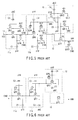
- FIG. 18 is a circuit diagram for illustrating an example of the construction of the booster section 22 in the circuit shown in FIG. 15 .
- the booster section 22 includes booster units (booster cells) 51 a, 51 b, booster unit 52 and output circuit section 53 .
- booster units 51 a, 51 b, 52 includes four MOS transistors (MOSFETs) and two capacitors and the output terminals of the booster units are respectively connected to the input terminals of the next-stage booster units.
- MOSFETs MOS transistors
- the booster unit 51 a includes P-channel MOS transistors QP 31 , QP 32 , QP 41 , QP 42 and capacitors C 31 , C 32 .
- One-side ends of the current paths of the MOS transistors QP 31 , QP 32 are connected to the ground node GND.
- the other end of the current path of the MOS transistor QP 32 is connected to the gate of the MOS transistor QP 31 and the gate thereof is connected to the other end of the current path of the MOS transistor QP 31 .
- One electrode of the capacitor C 31 is connected to the other end of the current path of the MOS transistor QP 31 and the other electrode of the capacitor C 31 is supplied with a clock signal phi 1 .
- One electrode of the capacitor C 32 is connected to the gate of the MOS transistor QP 31 and the other electrode of the capacitor C 32 is supplied with a clock signal phi 3 .
- the current path of the MOS transistor QP 41 is connected between the gate of the MOS transistor QP 32 and the ground node GND and the gate of the MOS transistor QP 41 is supplied with an internal reset signal RSTHB output from the reset signal generating section 21 .
- the current path of the MOS transistor QP 42 is connected between the gate of the MOS transistor QP 31 and the ground node GND and the gate of the MOS transistor QP 42 is supplied with the internal reset signal RSTHB.
- the booster unit 51 b includes P-channel MOS transistors QP 33 , QP 34 , QP 43 , QP 44 and capacitors C 33 , C 34 .
- One-side ends of the current paths of the MOS transistors QP 33 , QP 34 are connected to the other end of the current path of the MOS transistor QP 31 .
- the other end of the current path of the MOS transistor QP 34 is connected to the gate of the MOS transistor QP 33 and the gate thereof is connected to the other end of the current path of the MOS transistor QP 33 .
- One electrode of the capacitor C 33 is connected to the other end of the current path of the MOS transistor QP 33 and the other electrode of the capacitor C 33 is supplied with a clock signal phi 2 .
- One electrode of the capacitor C 34 is connected to the gate of the MOS transistor QP 33 and the other electrode of the capacitor C 34 is supplied with a clock signal phi 4 .
- the current path of the MOS transistor QP 43 is connected between the gate of the MOS transistor QP 34 and the ground node GND and the gate of the MOS transistor QP 43 is supplied with the internal reset signal RSTHB.
- the current path of the MOS transistor QP 44 is connected between the gate of the MOS transistor QP 33 and the ground node GND and the gate of the MOS transistor QP 44 is supplied with the internal reset signal RSTHB.
- the booster unit 52 includes P-channel MOS transistors QP 35 , QP 36 , QP 45 , QP 46 and capacitors C 35 , C 36 .
- One-side ends of the current paths of the MOS transistors QP 35 , QP 36 are connected to the other end of the current path of the MOS transistor QP 33 .
- the other end of the current path of the MOS transistor QP 36 is connected to the gate of the MOS transistor QP 35 and the gate thereof is connected to the other end of the current path of the MOS transistor QP 35 .
- One electrode of the capacitor C 35 is connected to the other end of the current path of the MOS transistor QP 35 and the other electrode of the capacitor C 35 is supplied with the clock signal phi 1 .
- One electrode of the capacitor C 36 is connected to the gate of the MOS transistor QP 35 and the other electrode of the capacitor C 36 is supplied with the clock signal phi 3 .
- the current path of the MOS transistor QP 45 is connected between the gate of the MOS transistor QP 35 and the ground node GND and the gate of the MOS transistor QP 45 is supplied with the internal reset signal RSTHB.
- the current path of the MOS transistor QP 46 is connected between the gate of the MOS transistor QP 36 and the ground node GND and the gate of the MOS transistor QP 46 is supplied with the internal reset signal RSTHB.
- the output circuit section 53 includes a P-channel MOS transistor QP 37 .
- One end of the current path of the MOS transistor QP 37 is connected to the other end of the current path of the MOS transistor QP 33 and the gate of the MOS transistor QP 37 is connected to the gate of the MOS transistor QP 35 .
- the boosted negative voltage VBB is output from the other end of the current path of the MOS transistor QP 37 .
- the circuit construction of the booster section 22 is basically the same as that of the circuit shown in FIG. 7, but in this circuit, an output signal of the reset signal generating section 21 is used as the internal reset signal RSTHB supplied to the gates of the resetting MOS transistors QP 41 to QP 46 .
- the reset signal generating section 21 generates the internal reset signal RSTHB by using the negative voltage VBB output from the booster section 22 .
- FIG. 19 is a timing chart for illustrating the operation of the booster circuit shown in FIGS. 15 to 18 .
- the gate voltage VG of the MOS transistor QP 37 and the output voltage VBB are gradually lowered for each cycle of the clock signals. If the output voltage VBB is lowered to a desired boosted level Vneg and a reset signal RST is input, then an internal reset signal RSTHB is created from the reset signal RST to drive the resetting MOS transistors QP 41 to QP 46 so as to set the gate potentials of the MOS transistors QP 31 to QP 37 to the ground potential (0 V).
- a switching signal SWN is set to the negative boosted level Vneg to interrupt the transistor section 23 .
- the output voltage VBB keeps the negative boosted level Vneg.
- the output voltage VBB of the booster section 22 is used to generate the reset signal, it becomes easy to generate a reset signal having an amplitude between the ground potential and a preset negative boosted potential only by use of the electrostatic capacitance and some logic circuits. Therefore, it becomes unnecessary to use a separate negative voltage generating circuit and an increase in the circuit scale can be suppressed and the control operation can be simplified.
- the booster circuit used in the flash memory system is explained as an example, but this invention is not limited to a semiconductor memory device and can be generally applied to a semiconductor integrated circuit device.
- FIGS. 20 to 22 are diagrams for illustrating a booster circuit according to a second embodiment of this invention and show an example in which this invention is applied to a four-phase type positive voltage generating booster circuit.
- the gate nodes of the internal transistors are reset to the VCC level by applying the output voltage VPP of the booster circuit to the gates of the resetting MOS transistors.
- the four-phase type positive voltage generating booster circuit shown in FIG. 20 includes a reset signal generating section 41 , booster section 42 and transistor section 43 .
- the transistor section 43 is connected between the output terminal of the booster section 42 and another circuit and ON/OFF-controlled by a switching signal SWP to supply or interrupt supply of the positive voltage VPP output from the booster section 42 to the other circuit used as a load.
- the reset signal generating section 41 includes a reset pulse generator 44 , discharge circuit 45 and capacitor 46 .
- the reset pulse generator 44 includes a high-level shifter 47 and inverter circuits 48 , 49 .
- the output terminals of the high-level shifter 47 and inverter circuits 48 , 49 are respectively connected to the input terminals of the next-stage circuits and they are operated on voltage between the positive boosted voltage VPP output from the booster circuit 42 and the ground node GND.
- the reset signal RST is supplied to the input terminal IN of the high-level shifter 47 , a signal output from the output terminal OUT of the high-level shifter 47 is supplied to the input terminal of the inverter circuit 48 , and a signal output from the inverter circuit 48 is supplied to the input terminal of the inverter circuit 49 .
- An output signal of the inverter circuit 49 is output as the internal reset signal RSTH.
- the internal reset signal RSTH is set at 0 V when the reset signal RST is set at the low level and it is set at the VPP level when the reset signal is set at the high level.
- the discharge circuit 45 includes a high-level shifter 50 , inverter circuits 51 , 52 and N-channel MOS transistor QN 80 .
- the output terminals of the high-level shifter 50 , inverter circuits 51 , 52 are respectively connected to the output terminals of the next-stage circuits and they are operated on voltage between the positive boosted voltage VPP output from the booster circuit 42 and the ground node GND.
- the discharge signal GNDEN is supplied to the input terminal IN of the high-level shifter 50 , a signal output from the output terminal OUT of the high-level shifter 50 is supplied to the input terminal of the inverter circuit 51 , and a signal output from the inverter circuit 51 is supplied to the input terminal of the inverter circuit 52 .
- An output signal of the inverter circuit 52 is supplied to the gate of the MOS transistor QN 80 .
- One end of the current path of the MOS transistor QN 80 is connected to a power supply line 53 to which the output voltage VPP of the booster section 42 is supplied and the other end thereof is connected to the power supply VCC.
- the capacitor 46 is connected between the power supply line 53 and the power supply VCC. Like the first embodiment, the capacitor 46 is a parasitic capacitor or a capacitor having a capacitance larger than or approximately equal to the whole gate capacitance associated with the gates of the N-channel MOS transistors in the booster section 42 to which the internal reset signal RSTH is input. As the capacitor 46 , a gate capacitor can be used or an electrostatic capacitor between two polysilicon layers, between two metal layers or between a polysilicon layer and a metal layer can be used.
- a large parasitic capacitance such as a PN junction capacitance in a portion in which the power supply line 53 is wired or an overlap capacitance between the gate electrode of the MOS transistor and the source region may be associated with the power supply line 53 to which the boosted voltage VPP is supplied in some cases. In such a case, the externally attached capacitor 46 becomes unnecessary.
- the reason why a capacitance larger than or approximately equal to the whole gate capacitance associated with the gates of the N-channel MOS transistors to which the internal reset signal RSTH is input is necessary is that the ON-resistance of the N-channel MOS transistor can be suppressed to a sufficiently small value even when the voltage VPP on one electrode side of the capacitor 46 is divided by the gate capacitance at the reset time.
- FIG. 21 is a circuit diagram for illustrating an example of the construction of the booster section 42 in the circuit shown in FIG. 20 .
- the circuit includes N-channel MOS transistors QN 31 to QN 37 , QN 41 to QN 46 instead of the P-channel MOS transistors QP 31 to QP 37 , QP 41 to QP 46 in the circuit shown in FIG. 18 .
- the internal reset signal RSTH output from the reset signal generating section 41 is supplied to the gates of the MOS transistors QN 41 to QN 46 . Further, one-side ends of the current paths of the resetting MOS transistors QN 41 to QN 46 are connected to the power supply VCC instead of the ground node.
- the gate nodes of the internal transistors are reset to the VCC level by applying the output voltage VPP of the booster section 42 to the gates of the resetting MOS transistors QN 41 to QN 46 . Therefore, since the gate node of the internal transistor is started to be boosted from the VCC level, an amount of charges required for the boosting operation can be reduced by VCC in comparison with a case wherein the gate node of the internal transistor is reset to 0 V.
- FIG. 23 illustrates a booster circuit according to a third embodiment of this invention and concretely shows another example of the construction of the booster section 22 of the first embodiment shown in FIG. 15 . That is, the capacitors C 31 to C 36 in the circuit shown in FIG. 18 are respectively constructed by two series-connected capacitors C 31 - 1 , C 31 - 2 to C 36 - 1 , C 36 - 2 and resetting MOS transistors QP 100 to QP 105 are respectively connected between connection nodes of the capacitors C 31 - 1 , C 31 - 2 to C 36 - 1 , C 36 - 2 and the ground node GND.
- the third embodiment is made by taking the following point into consideration. That is, an internal voltage of the booster circuit becomes higher than an output voltage thereof. Therefore, there occurs a possibility that the maximum input voltage may exceed the breakdown voltage of an insulating film of the capacitor when the thickness of the insulating film is small.
- a capacitor having an insulating film whose breakdown voltage is sufficiently high but in this case, it cannot be formed in the same process as that for forming a capacitor having a thin insulating film as in a semiconductor memory device, for example, and the manufacturing process becomes complicated. Therefore, in this embodiment, the capacitors C 31 - 1 , C 31 - 2 to C 36 - 1 , C 36 - 1 with thin insulating films which are serially connected are used.
- MOS capacitors are used as the capacitors C 31 - 1 , C 31 - 2 to C 36 - 1 , C 36 - 1 , a PN junction is formed in each connection node of the two capacitors. It is necessary to reset the connection node without fail, but it cannot be reset if a reset signal having an amplitude of the power supply voltage VCC is used as in the prior art.
- the connection nodes of the capacitors C 31 - 1 , C 31 - 2 to C 36 - 1 , C 36 - 1 can be reset without fail by using a reset signal RSTHB having an amplitude between a boosted negative voltage VBB and a ground potential.
- each of the capacitors C 31 - 1 to C 36 - 1 in the circuit of FIG. 21 by use of two series-connected capacitors and connect a resetting MOS transistor between the connection node of the capacitors and the power supply VCC.
- the gate node of the internal transistor can be relatively easily reset.
- a booster circuit which has a construction for resetting the gate node of the transistor having charges left behind therein and can suppress an increase in the circuit scale and in which the control operation can be simplified.
Landscapes
- Engineering & Computer Science (AREA)
- Power Engineering (AREA)
- Dc-Dc Converters (AREA)
- Read Only Memory (AREA)
- Logic Circuits (AREA)
- Manipulation Of Pulses (AREA)
Priority Applications (1)
| Application Number | Priority Date | Filing Date | Title |
|---|---|---|---|
| US10/212,062 US6614699B2 (en) | 2000-03-22 | 2002-08-06 | Booster circuit for raising voltage by sequentially transferring charges from input terminals of booster units to output terminals thereof in response to clock signals having different phases |
Applications Claiming Priority (2)
| Application Number | Priority Date | Filing Date | Title |
|---|---|---|---|
| JP2000080410A JP3872927B2 (ja) | 2000-03-22 | 2000-03-22 | 昇圧回路 |
| JP2000-080410 | 2000-03-22 |
Related Child Applications (1)
| Application Number | Title | Priority Date | Filing Date |
|---|---|---|---|
| US10/212,062 Division US6614699B2 (en) | 2000-03-22 | 2002-08-06 | Booster circuit for raising voltage by sequentially transferring charges from input terminals of booster units to output terminals thereof in response to clock signals having different phases |
Publications (2)
| Publication Number | Publication Date |
|---|---|
| US20010033515A1 US20010033515A1 (en) | 2001-10-25 |
| US6456541B2 true US6456541B2 (en) | 2002-09-24 |
Family
ID=18597515
Family Applications (2)
| Application Number | Title | Priority Date | Filing Date |
|---|---|---|---|
| US09/812,573 Expired - Lifetime US6456541B2 (en) | 2000-03-22 | 2001-03-21 | Booster circuit for raising voltage by sequentially transferring charges from input terminals of booster units to output terminals thereof in response to clock signals having different phases |
| US10/212,062 Expired - Lifetime US6614699B2 (en) | 2000-03-22 | 2002-08-06 | Booster circuit for raising voltage by sequentially transferring charges from input terminals of booster units to output terminals thereof in response to clock signals having different phases |
Family Applications After (1)
| Application Number | Title | Priority Date | Filing Date |
|---|---|---|---|
| US10/212,062 Expired - Lifetime US6614699B2 (en) | 2000-03-22 | 2002-08-06 | Booster circuit for raising voltage by sequentially transferring charges from input terminals of booster units to output terminals thereof in response to clock signals having different phases |
Country Status (2)
| Country | Link |
|---|---|
| US (2) | US6456541B2 (enExample) |
| JP (1) | JP3872927B2 (enExample) |
Cited By (11)
| Publication number | Priority date | Publication date | Assignee | Title |
|---|---|---|---|---|
| US6614699B2 (en) * | 2000-03-22 | 2003-09-02 | Kabushiki Kaisha Toshiba | Booster circuit for raising voltage by sequentially transferring charges from input terminals of booster units to output terminals thereof in response to clock signals having different phases |
| US20040240271A1 (en) * | 2000-05-25 | 2004-12-02 | Kabushiki Kaisha Toshiba | Boosted voltage generating circuit and semiconductor memory device having the same |
| US20050077950A1 (en) * | 2003-10-14 | 2005-04-14 | Robinson Curtis B. | Negative charge pump |
| US20060062169A1 (en) * | 2000-06-16 | 2006-03-23 | Mitsubishi Denki Kabushiki Kaisha | Dynamic bandwidth assignment system and dynamic bandwidth assignment method capable of reducing cell transmission delay |
| US20060067154A1 (en) * | 2004-09-24 | 2006-03-30 | Ferdinando Bedeschi | Biasing circuit for use in a non-volatile memory device |
| US7053945B1 (en) * | 2000-07-26 | 2006-05-30 | Micron Technolopgy, Inc. | Image sensor having boosted reset |
| US20060290414A1 (en) * | 2005-06-24 | 2006-12-28 | Samsung Electronics Co., Ltd. | Charge pump circuit and semiconductor memory device having the same |
| US20070146054A1 (en) * | 2005-12-22 | 2007-06-28 | Seiji Yamahira | Booster circuit |
| US20070241808A1 (en) * | 2006-04-12 | 2007-10-18 | Hynix Semiconductor Inc. | High voltage pumping device |
| US20080024199A1 (en) * | 2006-07-28 | 2008-01-31 | Hirokazu Miyazaki | Step-up booster circuit |
| US20100188137A1 (en) * | 2009-01-29 | 2010-07-29 | Makoto Mitani | Boosting circuit |
Families Citing this family (17)
| Publication number | Priority date | Publication date | Assignee | Title |
|---|---|---|---|---|
| CN1219352C (zh) | 2001-12-17 | 2005-09-14 | 松下电器产业株式会社 | 放大电路 |
| US6919236B2 (en) * | 2002-03-21 | 2005-07-19 | Advanced Micro Devices, Inc. | Biased, triple-well fully depleted SOI structure, and various methods of making and operating same |
| US6878981B2 (en) * | 2003-03-20 | 2005-04-12 | Tower Semiconductor Ltd. | Triple-well charge pump stage with no threshold voltage back-bias effect |
| CN100423421C (zh) * | 2003-05-13 | 2008-10-01 | 富士通株式会社 | 半导体集成电路装置 |
| US7323926B2 (en) * | 2004-12-21 | 2008-01-29 | Macronix International Co., Ltd. | Charge pump circuit |
| KR100732756B1 (ko) * | 2005-04-08 | 2007-06-27 | 주식회사 하이닉스반도체 | 전압 펌핑장치 |
| US7512015B1 (en) * | 2006-07-17 | 2009-03-31 | Lattice Semiconductor Corporation | Negative voltage blocking for embedded memories |
| US7619945B2 (en) * | 2006-08-18 | 2009-11-17 | Unity Semiconductor Corporation | Memory power management |
| US8232833B2 (en) | 2007-05-23 | 2012-07-31 | Silicon Storage Technology, Inc. | Charge pump systems and methods |
| US7592857B2 (en) * | 2007-12-21 | 2009-09-22 | G-Time Electronic Co., Ltd. | Charge pump circuit |
| JP5361346B2 (ja) * | 2008-11-21 | 2013-12-04 | 株式会社東芝 | 半導体集積回路 |
| JP5315087B2 (ja) * | 2009-02-20 | 2013-10-16 | セイコーインスツル株式会社 | 昇圧回路 |
| US9111601B2 (en) | 2012-06-08 | 2015-08-18 | Qualcomm Incorporated | Negative voltage generators |
| US9391597B2 (en) | 2013-11-12 | 2016-07-12 | Macronix International Co., Ltd. | Boost circuit |
| TWI559685B (zh) * | 2013-11-21 | 2016-11-21 | 旺宏電子股份有限公司 | 升壓電路及控制升壓信號之輸出之方法 |
| CN104682701B (zh) * | 2013-11-26 | 2017-04-26 | 旺宏电子股份有限公司 | 升压电路 |
| US11437097B2 (en) * | 2020-12-09 | 2022-09-06 | Micron Technology, Inc. | Voltage equalization for pillars of a memory array |
Citations (4)
| Publication number | Priority date | Publication date | Assignee | Title |
|---|---|---|---|---|
| JPH03129744A (ja) * | 1989-07-21 | 1991-06-03 | Nec Corp | 電荷転送装置 |
| US5856918A (en) * | 1995-11-08 | 1999-01-05 | Sony Corporation | Internal power supply circuit |
| US20010017566A1 (en) * | 2000-02-25 | 2001-08-30 | Nec Corporation | Charge pump type voltage conversion circuit having small ripple voltage components |
| US6333670B1 (en) * | 1999-06-09 | 2001-12-25 | Mitsubishi Denki Kabushiki Kaisha | Semiconductor device capable of stably generating internal voltage with low supply voltage |
Family Cites Families (5)
| Publication number | Priority date | Publication date | Assignee | Title |
|---|---|---|---|---|
| TW231343B (enExample) * | 1992-03-17 | 1994-10-01 | Hitachi Seisakusyo Kk | |
| JPH07130175A (ja) * | 1993-09-10 | 1995-05-19 | Toshiba Corp | 半導体記憶装置 |
| JP3497708B2 (ja) * | 1997-10-09 | 2004-02-16 | 株式会社東芝 | 半導体集積回路 |
| JP3872927B2 (ja) * | 2000-03-22 | 2007-01-24 | 株式会社東芝 | 昇圧回路 |
| JP5041631B2 (ja) * | 2001-06-15 | 2012-10-03 | ルネサスエレクトロニクス株式会社 | 半導体記憶装置 |
-
2000
- 2000-03-22 JP JP2000080410A patent/JP3872927B2/ja not_active Expired - Fee Related
-
2001
- 2001-03-21 US US09/812,573 patent/US6456541B2/en not_active Expired - Lifetime
-
2002
- 2002-08-06 US US10/212,062 patent/US6614699B2/en not_active Expired - Lifetime
Patent Citations (4)
| Publication number | Priority date | Publication date | Assignee | Title |
|---|---|---|---|---|
| JPH03129744A (ja) * | 1989-07-21 | 1991-06-03 | Nec Corp | 電荷転送装置 |
| US5856918A (en) * | 1995-11-08 | 1999-01-05 | Sony Corporation | Internal power supply circuit |
| US6333670B1 (en) * | 1999-06-09 | 2001-12-25 | Mitsubishi Denki Kabushiki Kaisha | Semiconductor device capable of stably generating internal voltage with low supply voltage |
| US20010017566A1 (en) * | 2000-02-25 | 2001-08-30 | Nec Corporation | Charge pump type voltage conversion circuit having small ripple voltage components |
Non-Patent Citations (3)
| Title |
|---|
| Jinbo, Toshikatsu, et al., "A 5-V-Only 16-Mb Flash Memory with Sector Erase Mode", IEEE Journal Of Solid-State Circuits, vol. 27, No. 11. Nov. 1992. |
| Umezawa, Akira, et al., "A 5-V Only Operation 0.6-mum Flash EEPROM with Row Decoder Scheme in Triple-Well Structure", IEEE Journal of Solid-State Circuits, vol. 27, No. 11. Nov. 1992. |
| Umezawa, Akira, et al., "A 5-V Only Operation 0.6-μm Flash EEPROM with Row Decoder Scheme in Triple-Well Structure", IEEE Journal of Solid-State Circuits, vol. 27, No. 11. Nov. 1992. |
Cited By (24)
| Publication number | Priority date | Publication date | Assignee | Title |
|---|---|---|---|---|
| US6614699B2 (en) * | 2000-03-22 | 2003-09-02 | Kabushiki Kaisha Toshiba | Booster circuit for raising voltage by sequentially transferring charges from input terminals of booster units to output terminals thereof in response to clock signals having different phases |
| US7180796B2 (en) | 2000-05-25 | 2007-02-20 | Kabushiki Kaisha Toshiba | Boosted voltage generating circuit and semiconductor memory device having the same |
| US20040240271A1 (en) * | 2000-05-25 | 2004-12-02 | Kabushiki Kaisha Toshiba | Boosted voltage generating circuit and semiconductor memory device having the same |
| US7203120B2 (en) | 2000-05-25 | 2007-04-10 | Kabushiki Kaisha Toshiba | Boosted voltage generating circuit and semiconductor memory device having the same |
| US6996024B2 (en) * | 2000-05-25 | 2006-02-07 | Kabushiki Kaisha Toshiba | Boosted voltage generating circuit and semiconductor memory device having the same |
| US20060055452A1 (en) * | 2000-05-25 | 2006-03-16 | Kabushiki Kaisha Toshiba | Boosted voltage generating circuit and semiconductor memory device having the same |
| US20060055453A1 (en) * | 2000-05-25 | 2006-03-16 | Kabushiki Kaisha Toshiba | Boosted voltage generating circuit and semiconductor memory device having the same |
| US20060062169A1 (en) * | 2000-06-16 | 2006-03-23 | Mitsubishi Denki Kabushiki Kaisha | Dynamic bandwidth assignment system and dynamic bandwidth assignment method capable of reducing cell transmission delay |
| US20060192872A1 (en) * | 2000-07-26 | 2006-08-31 | Song Xue | Image sensor having boosted reset |
| US7233353B2 (en) | 2000-07-26 | 2007-06-19 | Micron Technology, Inc. | Image sensor having boosted reset |
| US7053945B1 (en) * | 2000-07-26 | 2006-05-30 | Micron Technolopgy, Inc. | Image sensor having boosted reset |
| US20050077950A1 (en) * | 2003-10-14 | 2005-04-14 | Robinson Curtis B. | Negative charge pump |
| US7149132B2 (en) * | 2004-09-24 | 2006-12-12 | Ovonyx, Inc. | Biasing circuit for use in a non-volatile memory device |
| US20060067154A1 (en) * | 2004-09-24 | 2006-03-30 | Ferdinando Bedeschi | Biasing circuit for use in a non-volatile memory device |
| US20060290414A1 (en) * | 2005-06-24 | 2006-12-28 | Samsung Electronics Co., Ltd. | Charge pump circuit and semiconductor memory device having the same |
| US7511559B2 (en) * | 2005-12-22 | 2009-03-31 | Panasonic Corporation | Booster circuit |
| US20070146054A1 (en) * | 2005-12-22 | 2007-06-28 | Seiji Yamahira | Booster circuit |
| US20070241808A1 (en) * | 2006-04-12 | 2007-10-18 | Hynix Semiconductor Inc. | High voltage pumping device |
| US7498866B2 (en) * | 2006-04-12 | 2009-03-03 | Hynix Semiconductor Inc. | High voltage pumping device |
| US20080024199A1 (en) * | 2006-07-28 | 2008-01-31 | Hirokazu Miyazaki | Step-up booster circuit |
| US7560977B2 (en) * | 2006-07-28 | 2009-07-14 | Oki Semiconductor Co., Ltd. | Step-up booster circuit |
| US20100188137A1 (en) * | 2009-01-29 | 2010-07-29 | Makoto Mitani | Boosting circuit |
| US7961035B2 (en) * | 2009-01-29 | 2011-06-14 | Seiko Instruments Inc. | Boosting circuit |
| TWI472136B (zh) * | 2009-01-29 | 2015-02-01 | Seiko Instr Inc | 昇壓電路 |
Also Published As
| Publication number | Publication date |
|---|---|
| US20010033515A1 (en) | 2001-10-25 |
| US20020196673A1 (en) | 2002-12-26 |
| JP2001268893A (ja) | 2001-09-28 |
| JP3872927B2 (ja) | 2007-01-24 |
| US6614699B2 (en) | 2003-09-02 |
Similar Documents
| Publication | Publication Date | Title |
|---|---|---|
| US6456541B2 (en) | Booster circuit for raising voltage by sequentially transferring charges from input terminals of booster units to output terminals thereof in response to clock signals having different phases | |
| US5140182A (en) | Plural stage voltage booster circuit with efficient electric charge transfer between successive stages | |
| US4916334A (en) | High voltage booster circuit for use in EEPROMs | |
| US5394372A (en) | Semiconductor memory device having charge-pump system with improved oscillation means | |
| US7020024B2 (en) | Methods and devices for increasing voltages on non-selected wordlines during erasure of a flash memory | |
| US8811093B2 (en) | Non-volatile memory device and a method of operating same | |
| US7706194B2 (en) | Charge pump circuit, semiconductor memory device, and method for driving the same | |
| US5581107A (en) | Nonvolatile semiconductor memory that eases the dielectric strength requirements | |
| US11373707B2 (en) | Method and apparatus for configuring array columns and rows for accessing flash memory cells | |
| US20160217864A1 (en) | Non-volatile Split Gate Memory Device And A Method Of Operating Same | |
| US11120881B2 (en) | Charge pump for use in non-volatile flash memory devices | |
| US6477092B2 (en) | Level shifter of nonvolatile semiconductor memory | |
| US6614292B1 (en) | Boosting circuit of semiconductor memory device | |
| JP3192344B2 (ja) | 半導体記憶装置 | |
| US6608782B2 (en) | Booster circuit capable of achieving a stable pump operation for nonvolatile semiconductor memory device | |
| US8483004B2 (en) | Semiconductor device with transistor storing data by change in level of threshold voltage | |
| US6134147A (en) | Non-volatile semiconductor memory device | |
| JPH0271499A (ja) | 半導体記憶装置 | |
| US6738292B2 (en) | Nonvolatile semiconductor storage device | |
| JP3392438B2 (ja) | 不揮発性半導体記憶装置 | |
| US6744672B2 (en) | Non-volatile semiconductor memory device capable of high-speed data reading | |
| JPH11250682A (ja) | 半導体記憶装置及びそれを用いた半導体装置 | |
| KR20000033908A (ko) | 스테이틱 번-인 테스트 회로를 구비한 반도체 메모리 장치 |
Legal Events
| Date | Code | Title | Description |
|---|---|---|---|
| AS | Assignment |
Owner name: KABUSHIKI KAISHA TOSHIBA, JAPAN Free format text: ASSIGNMENT OF ASSIGNORS INTEREST;ASSIGNOR:TANZAWA, TORU;REEL/FRAME:011674/0539 Effective date: 20010313 |
|
| STCF | Information on status: patent grant |
Free format text: PATENTED CASE |
|
| FPAY | Fee payment |
Year of fee payment: 4 |
|
| FEPP | Fee payment procedure |
Free format text: PAYOR NUMBER ASSIGNED (ORIGINAL EVENT CODE: ASPN); ENTITY STATUS OF PATENT OWNER: LARGE ENTITY |
|
| FPAY | Fee payment |
Year of fee payment: 8 |
|
| FPAY | Fee payment |
Year of fee payment: 12 |
|
| AS | Assignment |
Owner name: TOSHIBA MEMORY CORPORATION, JAPAN Free format text: ASSIGNMENT OF ASSIGNORS INTEREST;ASSIGNOR:KABUSHIKI KAISHA TOSHIBA;REEL/FRAME:043709/0035 Effective date: 20170706 |