US6150224A - Method of manufacturing a semiconductor device with a bipolar transistor - Google Patents
Method of manufacturing a semiconductor device with a bipolar transistor Download PDFInfo
- Publication number
- US6150224A US6150224A US09/393,944 US39394499A US6150224A US 6150224 A US6150224 A US 6150224A US 39394499 A US39394499 A US 39394499A US 6150224 A US6150224 A US 6150224A
- Authority
- US
- United States
- Prior art keywords
- mask
- electrically insulating
- layer
- insulating region
- semiconductor body
- Prior art date
- Legal status (The legal status is an assumption and is not a legal conclusion. Google has not performed a legal analysis and makes no representation as to the accuracy of the status listed.)
- Expired - Lifetime
Links
Images
Classifications
-
- H—ELECTRICITY
- H10—SEMICONDUCTOR DEVICES; ELECTRIC SOLID-STATE DEVICES NOT OTHERWISE PROVIDED FOR
- H10D—INORGANIC ELECTRIC SEMICONDUCTOR DEVICES
- H10D10/00—Bipolar junction transistors [BJT]
- H10D10/01—Manufacture or treatment
- H10D10/051—Manufacture or treatment of vertical BJTs
- H10D10/054—Forming extrinsic base regions on silicon substrate after insulating device isolation in vertical BJTs having single crystalline emitter, collector or base regions
-
- H—ELECTRICITY
- H10—SEMICONDUCTOR DEVICES; ELECTRIC SOLID-STATE DEVICES NOT OTHERWISE PROVIDED FOR
- H10D—INORGANIC ELECTRIC SEMICONDUCTOR DEVICES
- H10D10/00—Bipolar junction transistors [BJT]
- H10D10/01—Manufacture or treatment
- H10D10/021—Manufacture or treatment of heterojunction BJTs [HBT]
Definitions
- the invention relates to a method of manufacturing a semiconductor device comprising a semiconductor body with a bipolar transistor including a base, an emitter and a collector, said base being formed by providing the semiconductor body with a doped semiconducting layer which locally borders on a monocrystalline part of the semiconductor body where it forms a first semiconductor region which is monocrystalline and constitutes the base of the transistor, and which semiconductive layer borders, outside said base, on a non-monocrystalline part of the semiconductor body where it forms a second semiconductor region which is not monocrystalline and which constitutes a connection region of the base, the non-monocrystalline part of the semiconductor body being obtained by covering the semiconductor body with a mask and replacing, on either side thereof, a part of the semiconductor body by an electrically insulating region, and by providing the electrically insulating region with a polycrystalline semiconducting layer before the provision of the semiconducting layer.
- Such a method is known from European patent application, filed by the current applicant (PHN 17.066) under application no. 98202894.6 on Aug. 31, 1998.
- a description is given of a method for the manufacture of a so-called differential bipolar transistor.
- Such a transistor is obtained by providing a semiconducting layer on a crystalline and a non-crystalline part of the semiconductor body, which forms at said locations, respectively, a crystalline semiconductor region, the base of the transistor, and a non-crystalline semiconductor region, a connecting region of the base.
- the crystalline part of the semiconductor body forms the collector, and in the semiconducting layer the emitter is formed at the location of the base.
- a drawback of the known method is that it is relatively laborious, partly because a photolithographic step followed by an etch step is necessary to form an aperture in the polycrystalline layer above the collector.
- a method in accordance with the invention is characterized in that the polycrystalline layer is selectively provided on the electrically insulating region, use being made of the mask to form the electrically insulating region.
- the method in accordance with the invention is much simpler than the known method. Additional photolithographic and etch steps are not necessary to (re-)expose the collector.
- the use of the mask employed for forming the electrically insulating region has an important additional advantage which is connected with the following surprising realization: by applying chemical-mechanical polishing during the selective application of the polycrystalline layer, said polycrystalline layer can be provided in the same manner as the electrically insulating region, thereby making its manufacture easy.
- the mask is, for example, a nitride mask which, as in the known method, can be used to form so-called LOCOS oxide which forms the electrically insulating region on either side of the collector.
- Re-exposing the mask can take place simultaneously with leveling off the structure by means of CMP. It can also be achieved by means of etching after the CMP treatment using an anisotropic etching technique, such as plasma etching.
- the electrically insulating region is formed by making grooves in the semiconductor body on either side of the mask, providing an electrically insulating layer in the grooves and on the mask, whereafter an electrically insulating layer is provided in the grooves and on the mask, and the resultant structure is leveled off by means of chemico-mechanical polishing, the mask remaining buried in the electrically insulating layer, whereafter the electrically insulating layer is removed to such an extent that the mask is re-exposed, whereafter a part of the resultant electrically insulating region is removed, the mask remaining intact.
- Such a method, in which chemico-mechanical polishing can also be used to form the electrically insulating region, keeps the method simple because both the electrically insulating region and the polycrystalline layer are formed in the same manner.
- the formation of the electrically insulating region in this manner results in a very flat structure, thereby substantially simplifying the subsequent selective provision in a similar manner of the polycrystalline semiconducting layer, since an electrically insulating region formed by so-called LOCOS oxide, results in a structure which is not very flat, thereby hampering the chemico-mechanical process to be carried out after the provision of the polycrystalline layer.
- This profile can be obtained by forming a recess in the structure using a wet-chemical etchant which is selective with respect to electrically insulating material.
- the mask can be exposed by means of the CMP step, but also by a separate (anisotropic) etch step after the structure has been leveled off by means of CMP, the mask still being buried in the insulating layer. If the anisotropic etch step is carried out using an etchant which etches the electrically insulating material in a selective manner with respect to the mask, then the additional advantage is obtained that no separate etch step is necessary to provide the structure, after exposure of the mask, with the profile necessary to apply the polycrystalline layer. Also in this case, a suitable technique for anisotropic (selective) etching is the plasma-etched technique. Finally, partly because of the absence of LOCOS oxide, the method of this variant can very suitably be used to manufacture transistors having very small dimensions.
- the mask used in this operation is preferably removed. This can be achieved in a simple manner by immersing the mask in an etchant which is selective with respect to the mask. As a result, the collector is re-exposed, and the semiconducting layer can be provided. Subsequently, the emitter can be formed so as to border on the base.
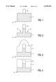
- FIGS. 1 through 10 are diagrammatic, cross-sectional views, at right angles to the thickness direction, of a semiconductor device with a bipolar transistor, at successive stages in the manufacture using a method in accordance with the invention.
- FIGS. 1 through 10 are diagrammatic, cross-sectional views, at right angles to the thickness direction, of a semiconductor device with a bipolar transistor, at successive stages in the manufacture using a method in accordance with the invention.
- FIG. 10 is a diagrammatic, cross-sectional view, at right angles to the thickness direction, of the finished device comprising a bipolar transistor.
- the semiconductor body 10 comprises (not shown in the drawing) a monocrystalline substrate of p + -type silicon covered with a 1 ⁇ m thick monocrystalline epitaxial layer 3 of n-type silicon with a doping concentration of 1 ⁇ 10 16 at/cm 3 which forms a collector 3 of the transistor.
- the epitaxial layer 3 accommodates a 0.3 ⁇ m recessed insulation region 8 which, in this case, includes silicon dioxide and surrounds the collector 3.
- a polycrystalline, p-type silicon layer 4 having a thickness of 50 nm and a doping concentration of, in this example, 1 ⁇ 10 20 at/cm 3 .
- an, in this case 150 nm thick, p-type semiconducting layer 1 which, in this case contains SiGe with 20 at. % germanium.
- the part 1A of the semiconducting layer 1 bordering on the collector 3 is monocrystalline and forms a base 1A of the transistor.
- the remaining part 1B of the semiconducting layer 1 is polycrystalline, borders on the polycrystalline layer 4 and forms a connecting region 1B of the base 1A of the transistor.
- the doping concentration is 1 ⁇ 10 19 at/cm 3
- the connecting region 1B the doping concentration is higher and amounts to 1 ⁇ 10 20 at/cm 3 .
- LPCVD Low Pressure Chemical Vapor Deposition
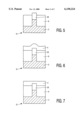
- the oxide layer 8 is subjected to a chemico-mechanical polishing so as to ensure that the resultant structure is flat and the surface of the (remaining part) of the mask 20 is re-exposed.
- a suitable slurry is, for example, ss12 by Cabbot.
- a part of the insulation oxide 8 is removed again by means of an etchant comprising hydrogen fluoride, in which process the mask 20 is not attached and projects 0.1 ⁇ m above the surface of the semiconductor body 10 after the etch process.
- the electrically insulating region 8 is subsequently selectively provided with a polycrystalline semiconducting layer 4, in which process use is made of the mask 20 which was used to form the electrically insulating region 8.
- the method in accordance with the invention is much simpler than the known method.
- additional photolithography and etching, as in the known method are not necessary to remove (again) the polycrystalline layer 1 above the collector 3.
- a chemico-mechanical polishing technique becomes very suitable to obtain the desired result.
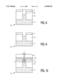
- the surface of the semiconductor body 10 is first provided with a several tens of micrometers thick polycrystalline semiconducting layer 4, in this case by means of LPCVD from a gas mixture containing silane and hydrogen. Subsequently, (see FIG. 7) the polycrystalline layer 4 is removed by means of chemico-mechanical polishing to such an extent the resultant structure is flat. At this stage, the mask 20 is still buried in the polycrystalline layer 4. In this process, use is made of the same slurry as in the above-described chemico-mechanical polishing step. It is alternatively possible, however, to use a different slurry which is more specially developed for etching polycrystalline silicon. Next, (see FIG. 6)
- the mask 20 is removed by means of etching, in this case by means of warm phosphoric acid, without the polycrystalline layer 4 and the collector 3 being attacked.
- the resultant structure is used to continue the manufacture of the transistor.
- the further content of the method used in this example can be summarized as follows (see FIG. 10): the application of the semiconducting layer 1, the provision above the base 1A of a further mask of silicon nitride, depositing an insulating layer 6 on said mask, followed by planarization of the structure by means of chemico-mechanical polishing, the removal of the further mask and providing polycrystalline silicon 7 in the resultant aperture, thus forming the emitter 2, which itself forms a connecting region for the emitter 2. Furthermore, the base 1A and the collector 3 are provided (via their connecting region) with connecting conductors.
- PPN 16.077 European patent application
- the geometry and dimensions of the various regions of the transistor may be chosen so as to be different.
- a device in accordance with the invention can also be a more complex device than a single bipolar transistor.
- the device may comprise a number of different active or passive components.
Landscapes
- Bipolar Transistors (AREA)
Applications Claiming Priority (2)
| Application Number | Priority Date | Filing Date | Title |
|---|---|---|---|
| EP98203054 | 1998-09-11 | ||
| EP98203054 | 1998-09-11 |
Publications (1)
| Publication Number | Publication Date |
|---|---|
| US6150224A true US6150224A (en) | 2000-11-21 |
Family
ID=8234106
Family Applications (1)
| Application Number | Title | Priority Date | Filing Date |
|---|---|---|---|
| US09/393,944 Expired - Lifetime US6150224A (en) | 1998-09-11 | 1999-09-10 | Method of manufacturing a semiconductor device with a bipolar transistor |
Country Status (5)
| Country | Link |
|---|---|
| US (1) | US6150224A (enExample) |
| EP (1) | EP1048066B1 (enExample) |
| JP (1) | JP2002525851A (enExample) |
| DE (1) | DE69935967T2 (enExample) |
| WO (1) | WO2000016392A1 (enExample) |
Cited By (1)
| Publication number | Priority date | Publication date | Assignee | Title |
|---|---|---|---|---|
| US6300210B1 (en) * | 1998-11-13 | 2001-10-09 | U.S. Philips Corporation | Method of manufacturing a semiconductor device comprising a bipolar transistor |
Citations (3)
| Publication number | Priority date | Publication date | Assignee | Title |
|---|---|---|---|---|
| EP0378794A1 (en) * | 1989-01-18 | 1990-07-25 | International Business Machines Corporation | Vertical bipolar transistor structure and method of manufacturing |
| US5106767A (en) * | 1990-12-07 | 1992-04-21 | International Business Machines Corporation | Process for fabricating low capacitance bipolar junction transistor |
| US5656514A (en) * | 1992-07-13 | 1997-08-12 | International Business Machines Corporation | Method for making heterojunction bipolar transistor with self-aligned retrograde emitter profile |
Family Cites Families (2)
| Publication number | Priority date | Publication date | Assignee | Title |
|---|---|---|---|---|
| US5117271A (en) * | 1990-12-07 | 1992-05-26 | International Business Machines Corporation | Low capacitance bipolar junction transistor and fabrication process therfor |
| DE19609933A1 (de) * | 1996-03-14 | 1997-09-18 | Daimler Benz Ag | Verfahren zur Herstellung eines Heterobipolartransistors |
-
1999
- 1999-08-31 DE DE69935967T patent/DE69935967T2/de not_active Expired - Lifetime
- 1999-08-31 WO PCT/EP1999/006416 patent/WO2000016392A1/en not_active Ceased
- 1999-08-31 JP JP2000570829A patent/JP2002525851A/ja active Pending
- 1999-08-31 EP EP99969180A patent/EP1048066B1/en not_active Expired - Lifetime
- 1999-09-10 US US09/393,944 patent/US6150224A/en not_active Expired - Lifetime
Patent Citations (3)
| Publication number | Priority date | Publication date | Assignee | Title |
|---|---|---|---|---|
| EP0378794A1 (en) * | 1989-01-18 | 1990-07-25 | International Business Machines Corporation | Vertical bipolar transistor structure and method of manufacturing |
| US5106767A (en) * | 1990-12-07 | 1992-04-21 | International Business Machines Corporation | Process for fabricating low capacitance bipolar junction transistor |
| US5656514A (en) * | 1992-07-13 | 1997-08-12 | International Business Machines Corporation | Method for making heterojunction bipolar transistor with self-aligned retrograde emitter profile |
Non-Patent Citations (1)
| Title |
|---|
| PHN 17,066, U.S. Ser. No. 09/387,629, Filed: Aug. 31, 1999. * |
Cited By (1)
| Publication number | Priority date | Publication date | Assignee | Title |
|---|---|---|---|---|
| US6300210B1 (en) * | 1998-11-13 | 2001-10-09 | U.S. Philips Corporation | Method of manufacturing a semiconductor device comprising a bipolar transistor |
Also Published As
| Publication number | Publication date |
|---|---|
| EP1048066B1 (en) | 2007-05-02 |
| DE69935967D1 (de) | 2007-06-14 |
| JP2002525851A (ja) | 2002-08-13 |
| EP1048066A1 (en) | 2000-11-02 |
| DE69935967T2 (de) | 2008-01-10 |
| WO2000016392A1 (en) | 2000-03-23 |
Similar Documents
| Publication | Publication Date | Title |
|---|---|---|
| US4502913A (en) | Total dielectric isolation for integrated circuits | |
| JP2554831B2 (ja) | 基板分離トレンチを形成するための半導体処理方法 | |
| EP0036111B1 (en) | Method for making fine deep dielectric isolation | |
| EP0039411B1 (en) | Process for fabricating an integrated pnp and npn transistor structure | |
| US4378630A (en) | Process for fabricating a high performance PNP and NPN structure | |
| JPH05102296A (ja) | 集積回路において平坦化した浅いトレンチ分離を製造する方法及びそれにより製造された構成体 | |
| US4829015A (en) | Method for manufacturing a fully self-adjusted bipolar transistor | |
| JP2720793B2 (ja) | 半導体装置の製造方法 | |
| US4661832A (en) | Total dielectric isolation for integrated circuits | |
| JPS6240858B2 (enExample) | ||
| JPH02296338A (ja) | 横型トランジスタ及びその製造方法 | |
| US6204098B1 (en) | Method of formation in a silicon wafer of an insulated well | |
| US6331470B1 (en) | Process for manufacturing a semiconductor material wafer having power regions dielectrically insulated from circuitry regions | |
| US4649630A (en) | Process for dielectrically isolated semiconductor structure | |
| JP3130511B2 (ja) | 半導体パワー集積回路の素子隔離構造及びその形成方法 | |
| US6150224A (en) | Method of manufacturing a semiconductor device with a bipolar transistor | |
| US5851901A (en) | Method of manufacturing an isolation region of a semiconductor device with advanced planarization | |
| US6403492B1 (en) | Method of manufacturing semiconductor devices with trench isolation | |
| JP3109549B2 (ja) | 半導体装置の製造方法 | |
| JPS6310895B2 (enExample) | ||
| JPH06291178A (ja) | 半導体装置の製造方法 | |
| EP0236811B1 (en) | Method of manufacturing semiconductor device | |
| JPH0729971A (ja) | 半導体装置の製造方法 | |
| JP3190144B2 (ja) | 半導体集積回路の製造方法 | |
| US6713361B2 (en) | Method of manufacturing a bipolar junction transistor including undercutting regions adjacent to the emitter region to enlarge the emitter region |
Legal Events
| Date | Code | Title | Description |
|---|---|---|---|
| AS | Assignment |
Owner name: U.S. PHILIPS CORPORATION, NEW YORK Free format text: ASSIGNMENT OF ASSIGNORS INTEREST;ASSIGNORS:TERPSTRA, DOEDE;EMONS, CATHARINA H.H.;REEL/FRAME:010307/0565;SIGNING DATES FROM 19990924 TO 19990928 |
|
| STCF | Information on status: patent grant |
Free format text: PATENTED CASE |
|
| FPAY | Fee payment |
Year of fee payment: 4 |
|
| AS | Assignment |
Owner name: NXP B.V., NETHERLANDS Free format text: ASSIGNMENT OF ASSIGNORS INTEREST;ASSIGNOR:U.S. PHILIPS CORPORATION;REEL/FRAME:018635/0755 Effective date: 20061127 |
|
| FPAY | Fee payment |
Year of fee payment: 8 |
|
| FPAY | Fee payment |
Year of fee payment: 12 |
|
| AS | Assignment |
Owner name: PHILIPS SEMICONDUCTORS INTERNATIONAL B.V., NETHERL Free format text: ASSIGNMENT OF ASSIGNORS INTEREST;ASSIGNOR:KONINKLIJKE PHILIPS ELECTRONICS N.V.;REEL/FRAME:043951/0127 Effective date: 20060928 Owner name: NXP B.V., NETHERLANDS Free format text: CHANGE OF NAME;ASSIGNOR:PHILIPS SEMICONDUCTORS INTERNATIONAL B.V.;REEL/FRAME:043951/0611 Effective date: 20060929 |