EP1048066B1 - Method of manufacturing a semiconductor device with a bipolar transistor - Google Patents
Method of manufacturing a semiconductor device with a bipolar transistor Download PDFInfo
- Publication number
- EP1048066B1 EP1048066B1 EP99969180A EP99969180A EP1048066B1 EP 1048066 B1 EP1048066 B1 EP 1048066B1 EP 99969180 A EP99969180 A EP 99969180A EP 99969180 A EP99969180 A EP 99969180A EP 1048066 B1 EP1048066 B1 EP 1048066B1
- Authority
- EP
- European Patent Office
- Prior art keywords
- mask
- electrically insulating
- layer
- insulating region
- base
- Prior art date
- Legal status (The legal status is an assumption and is not a legal conclusion. Google has not performed a legal analysis and makes no representation as to the accuracy of the status listed.)
- Expired - Lifetime
Links
- 239000004065 semiconductor Substances 0.000 title claims abstract description 41
- 238000004519 manufacturing process Methods 0.000 title claims abstract description 15
- 238000000034 method Methods 0.000 claims abstract description 47
- 238000005498 polishing Methods 0.000 claims abstract description 13
- VYPSYNLAJGMNEJ-UHFFFAOYSA-N Silicium dioxide Chemical compound O=[Si]=O VYPSYNLAJGMNEJ-UHFFFAOYSA-N 0.000 claims description 12
- 238000005530 etching Methods 0.000 claims description 11
- 239000000463 material Substances 0.000 claims description 6
- 239000000377 silicon dioxide Substances 0.000 claims description 6
- 235000012239 silicon dioxide Nutrition 0.000 claims description 6
- 229910052581 Si3N4 Inorganic materials 0.000 claims description 4
- 230000015572 biosynthetic process Effects 0.000 claims description 4
- HQVNEWCFYHHQES-UHFFFAOYSA-N silicon nitride Chemical compound N12[Si]34N5[Si]62N3[Si]51N64 HQVNEWCFYHHQES-UHFFFAOYSA-N 0.000 claims description 4
- 230000008021 deposition Effects 0.000 abstract 1
- XUIMIQQOPSSXEZ-UHFFFAOYSA-N Silicon Chemical compound [Si] XUIMIQQOPSSXEZ-UHFFFAOYSA-N 0.000 description 9
- 229910052710 silicon Inorganic materials 0.000 description 9
- 239000010703 silicon Substances 0.000 description 9
- 229910021420 polycrystalline silicon Inorganic materials 0.000 description 5
- 239000002002 slurry Substances 0.000 description 4
- KWYUFKZDYYNOTN-UHFFFAOYSA-M Potassium hydroxide Chemical compound [OH-].[K+] KWYUFKZDYYNOTN-UHFFFAOYSA-M 0.000 description 3
- 238000009413 insulation Methods 0.000 description 3
- 238000004518 low pressure chemical vapour deposition Methods 0.000 description 3
- 238000000206 photolithography Methods 0.000 description 3
- 238000001020 plasma etching Methods 0.000 description 3
- NBIIXXVUZAFLBC-UHFFFAOYSA-N Phosphoric acid Chemical compound OP(O)(O)=O NBIIXXVUZAFLBC-UHFFFAOYSA-N 0.000 description 2
- 238000005229 chemical vapour deposition Methods 0.000 description 2
- 238000000151 deposition Methods 0.000 description 2
- 239000012777 electrically insulating material Substances 0.000 description 2
- 238000007521 mechanical polishing technique Methods 0.000 description 2
- 239000000203 mixture Substances 0.000 description 2
- 238000001451 molecular beam epitaxy Methods 0.000 description 2
- 229920005591 polysilicon Polymers 0.000 description 2
- 239000000758 substrate Substances 0.000 description 2
- KRHYYFGTRYWZRS-UHFFFAOYSA-N Fluorane Chemical compound F KRHYYFGTRYWZRS-UHFFFAOYSA-N 0.000 description 1
- UFHFLCQGNIYNRP-UHFFFAOYSA-N Hydrogen Chemical compound [H][H] UFHFLCQGNIYNRP-UHFFFAOYSA-N 0.000 description 1
- BLRPTPMANUNPDV-UHFFFAOYSA-N Silane Chemical compound [SiH4] BLRPTPMANUNPDV-UHFFFAOYSA-N 0.000 description 1
- 229910000577 Silicon-germanium Inorganic materials 0.000 description 1
- 229910000147 aluminium phosphate Inorganic materials 0.000 description 1
- 230000000295 complement effect Effects 0.000 description 1
- 239000004020 conductor Substances 0.000 description 1
- 238000005137 deposition process Methods 0.000 description 1
- 239000007789 gas Substances 0.000 description 1
- 229910052732 germanium Inorganic materials 0.000 description 1
- GNPVGFCGXDBREM-UHFFFAOYSA-N germanium atom Chemical compound [Ge] GNPVGFCGXDBREM-UHFFFAOYSA-N 0.000 description 1
- 239000001257 hydrogen Substances 0.000 description 1
- 229910052739 hydrogen Inorganic materials 0.000 description 1
- 229910000040 hydrogen fluoride Inorganic materials 0.000 description 1
- 238000002955 isolation Methods 0.000 description 1
- 238000010297 mechanical methods and process Methods 0.000 description 1
- 229910044991 metal oxide Inorganic materials 0.000 description 1
- 150000004706 metal oxides Chemical class 0.000 description 1
- 238000012986 modification Methods 0.000 description 1
- 230000004048 modification Effects 0.000 description 1
- 150000004767 nitrides Chemical class 0.000 description 1
- 230000003647 oxidation Effects 0.000 description 1
- 238000007254 oxidation reaction Methods 0.000 description 1
- 239000002245 particle Substances 0.000 description 1
- 229910000077 silane Inorganic materials 0.000 description 1
- 239000000126 substance Substances 0.000 description 1
Images
Classifications
-
- H—ELECTRICITY
- H10—SEMICONDUCTOR DEVICES; ELECTRIC SOLID-STATE DEVICES NOT OTHERWISE PROVIDED FOR
- H10D—INORGANIC ELECTRIC SEMICONDUCTOR DEVICES
- H10D10/00—Bipolar junction transistors [BJT]
- H10D10/01—Manufacture or treatment
- H10D10/051—Manufacture or treatment of vertical BJTs
- H10D10/054—Forming extrinsic base regions on silicon substrate after insulating device isolation in vertical BJTs having single crystalline emitter, collector or base regions
-
- H—ELECTRICITY
- H10—SEMICONDUCTOR DEVICES; ELECTRIC SOLID-STATE DEVICES NOT OTHERWISE PROVIDED FOR
- H10D—INORGANIC ELECTRIC SEMICONDUCTOR DEVICES
- H10D10/00—Bipolar junction transistors [BJT]
- H10D10/01—Manufacture or treatment
- H10D10/021—Manufacture or treatment of heterojunction BJTs [HBT]
Definitions
- the invention relates to a method of manufacturing a semiconductor device comprising a semiconductor body with a bipolar transistor including a base, an emitter and a collector, said base being formed by providing the semiconductor body with a doped semiconducting layer which locally borders on a monocrystalline part of the semiconductor body where it forms a first semiconductor region which is monocrystalline and constitutes the base of the transistor, and which semiconductive layer borders, outside said base, on a non-monocrystalline part of the semiconductor body where it forms a second semiconductor region which is not monocrystalline and which constitutes a connection region of the base, the non-monocrystalline part of the semiconductor body being obtained by covering the semiconductor body with a mask and replacing, on either side thereof, a part of the semiconductor body by an electrically insulating region, and by providing the electrically insulating region with a polycrystalline semiconducting layer before the provision of the semiconducting layer.
- Such a method is known from European patent application, filed by the current applicant (PHN 17.066) under application no. 98202894.6 on 31-08-1998, published as WO-A-0 013 227.
- This document falls under Art. 54(3)EPC.
- a description is given of a method for the manufacture of a so-called differential bipolar transistor.
- Such a transistor is obtained by providing a semiconducting layer on a crystalline and a non-crystalline part of the semiconductor body, which forms at said locations, respectively, a crystalline semiconductor region, the base of the transistor, and a non-crystalline semiconductor region, a connecting region of the base.
- the crystalline part of the semiconductor body forms the collector, and in the semiconducting layer the emitter is formed at the location of the base.
- the non-monocrystalline part of the semiconductor body is formed by an electrically insulating region which surrounds the collector and on which a polycrystalline semiconducting layer is situated which serves as the host layer during the provision of the semiconducting layer.
- a drawback of the known method is that it is relatively laborious, partly because a photolithographic step followed by an etch step is necessary to form an aperture in the polycrystalline layer above the collector.
- EP-A-0378794 describes a method of manufacturing a self aligned bipolar transistor using planarization twice in order to form the extrinsic base polysilicon on -and self-aligned with- device insulation.
- US-A-5656514 describes a method of manufacturing a self aligned bipolar transistor, where the connecting polysilicon is formed on the device isolation. Then, the intrinsic base layer is formed.
- a method in accordance with the invention is characterized in that the polycrystalline layer is selectively provided on the electrically insulating region, use being made of the mask to form the electrically insulating region.
- the method in accordance with the invention is much simpler than the known method. Additional photolithographic and etch steps are not necessary to (re-)expose the collector.
- the use of the mask employed for forming the electrically insulating region has an important additional advantage which is connected with the following surprising realization: by applying chemico-mechanical polishing during the selective application of the polycrystalline layer, said polycrystalline layer can be provided in the same manner as the electrically insulating region, thereby making its manufacture easy.
- a method in accordance with the invention has the important advantage that the aperture which the polycrystalline semiconducting layer should have above the collector is formed in a self-recording manner relative to said collector.
- the dimensions of the transistor to be formed can be much better controlled, thus enabling, in particular, said dimensions to be very small and hence the transistor very fast.
- the polycrystalline semiconducting layer is provided onto the mask and the electrically insulating region, and the resulting structure is leveled off by means of chemico-mechanical polishing, the mask remaining buried in the polycrystalline semiconducting layer, and subsequently the polycrystalline semiconducting layer is removed to such an extent that the mask is re-exposed.
- a method in accordance with the invention is made simple by applying this technique.
- the mask is, for example, a nitride mask which, as in the known method, can be used to form so-called LOCOS oxide which forms the electrically insulating region on either side of the collector.
- Re-exposing the mask can take place simultaneously with leveling off the structure by means of CMP. It can also be achieved by means of etching after the CMP treatment using an anisotropic etching technique, such as plasma etching.
- the electrically insulating region is formed by making grooves in the semiconductor body on either side of the mask, providing an electrically insulating layer in the grooves and on the mask, whereafter an electrically insulating layer is provided in the grooves and on the mask, and the resultant structure is leveled off by means of chemico-mechanical polishing, the mask remaining buried in the electrically insulating layer, whereafter the electrically insulating layer is removed to such an extent that the mask is re-exposed, whereafter a part of the resultant electrically insulating region is removed, the mask remaining intact.
- Such a method, in which chemico-mechanical polishing can also be used to form the electrically insulating region, keeps the method simple because both the electrically insulating region and the polycrystalline layer are formed in the same manner.
- the formation of the electrically insulating region in this manner results in a very flat structure, thereby substantially simplifying the subsequent selective provision in a similar manner of the polycrystalline semiconducting layer, since an electrically insulating region formed by so-called LOCOS oxide, results in a structure which is not very flat, thereby hampering the chemico-mechanical process to be carried out after the provision of the polycrystalline layer.
- This profile can be obtained by forming a recess in the structure using a wet-chemical etchant which is selective with respect to electrically insulating material.
- the mask can be exposed by means of the CMP step, but also by a separate (anisotropic) etch step after the structure has been leveled off by means of CMP, the mask still being buried in the insulating layer. If the anisotropic etch step is carried out using an etchant which etches the electrically insulating material in a selective manner with respect to the mask, then the additional advantage is obtained that no separate etch step is necessary to provide the structure, after exposure of the mask, with the profile necessary to apply the polycrystalline layer. Also in this case, a suitable technique for anisotropic (selective) etching is the plasma-etched technique. Finally, partly because of the absence of LOCOS oxide, the method of this variant can very suitably be used to manufacture transistors having very small dimensions.
- the mask used in this operation is preferably removed. This can be achieved in a simple manner by immersing the mask in an etchant which is selective with respect to the mask. As a result, the collector is re-exposed, and the semiconducting layer can be provided. Subsequently, the emitter can be formed so as to border on the base.
- silicon dioxide is used as the material for the electrically insulating region
- silicon nitride is used as the material for the mask.
- These materials can be readily selectively removed relative to each other and relative to silicon. These materials can also very suitably be used in combination with the chemico-mechanical polishing technique.
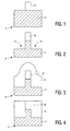
- Figs. 1 through 10 are diagrammatic, cross-sectional views, at right angles to the thickness direction, of a semiconductor device with a bipolar transistor, at successive stages in the manufacture using a method in accordance with the invention.
- FIGs. 1 through 10 are diagrammatic, cross-sectional views, at right angles to the thickness direction, of a semiconductor device with a bipolar transistor, at successive stages in the manufacture using a method in accordance with the invention.
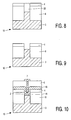
- Fig. 10 is a diagrammatic, cross-sectional view, at right angles to the thickness direction, of the finished device comprising a bipolar transistor.
- the semiconductor body 10 comprises (not shown in the drawing) a monocrystalline substrate of p + -type silicon covered with a 1 ⁇ m thick monocrystalline epitaxial layer 3 of n-type silicon with a doping concentration of 1 x 10 16 at/cm 3 which forms a collector 3 of the transistor.
- the epitaxial layer 3 accommodates a 0.3 ⁇ m recessed insulation region 8 which, in this case, includes silicon dioxide and surrounds the collector 3.
- a polycrystalline, p-type silicon layer 4 having a thickness of 50 nm and a doping concentration of, in this example, 1 x 10 20 at/cm 3 .
- an, in this case 150 nm thick, p-type semiconducting layer 1 which, in this case contains SiGe with 20 at.% germanium.
- the part 1A of the semiconducting layer 1 bordering on the collector 3 is monocrystalline and forms a base 1A of the transistor.
- the remaining part 1B of the semiconducting layer 1 is polycrystalline, borders on the polycrystalline layer 4 and forms a connecting region 1B of the base 1A of the transistor.
- the doping concentration is 1 x 10 19 at/cm 3
- the connecting region 1B the doping concentration is higher and amounts to 1 x 10 20 at/cm 3 .
- the semiconducting layer 1 there is a 0.3 ⁇ m thick insulating layer of silicon dioxide having a recessed portion above the base 1A, which is filled with an emitter connection 7 of n-type polycrystalline silicon whose doping concentration is approximately 10 21 at/cm 3 .
- an emitter 2 of the transistor which is recessed in the base 1A which is of the n-conductivity type, has a thickness of 40 nm and a doping concentration of approximately 10 20 at/cm 3 .
- the device further includes (not shown in the Figure) electrical connections of the connecting region 11 of the emitter 2, of the connecting region 1B of the base 1A and of a connecting region (not shown either in the drawing) of the collector 3.
- the width of the part of the semiconductor body shown in the drawing is several micrometers, the collector 3 and the base 1A have a width of approximately 1 ⁇ m, and the width of the emitter 2 and the emitter connection 7 is approximately 0.5 ⁇ m.
- a p-type silicon substrate (not shown in the drawing) is first provided with an epitaxial n-type silicon layer 3 (see Fig. 1).
- This n-type silicon layer is provided with a mask 20, which in this case is formed from a 200 nm thick silicon nitride layer 20 by means of photolithography and etching.
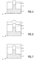
- a mask 20 By means of plasma etching (see Fig. 2), 0.3 ⁇ m deep grooves 21 are formed in the semiconductor body 10 on either side of the mask 20. Subsequently, (see Fig.
- LPCVD Low Pressure Chemical Vapor Deposition
- the oxide layer 8 is subjected to a chemico-mechanical polishing so as to ensure that the resultant structure is flat and the surface of the (remaining part) of the mask 20 is re-exposed.
- a suitable slurry is, for example, ss12 by Cabbot.
- a part of the insulation oxide 8 is removed again by means of an etchant comprising hydrogen fluoride, in which process the mask 20 is not attached and projects 0.1 ⁇ m above the surface of the semiconductor body 10 after the etch process.
- the electrically insulating region 8 is subsequently selectively provided with a polycrystalline semiconducting layer 4, in which process use is made of the mask 20 which was used to form the electrically insulating region 8.
- the method in accordance with the invention is much simpler than the known method.
- additional photolithography and etching, as in the known method are not necessary to remove (again) the polycrystalline layer 1 above the collector 3.
- a chemico-mechanical polishing technique becomes very suitable to obtain the desired result.
- Another important advantage of a method in accordance with the invention is that the aperture in the polycrystalline semiconducting layer 4 above the collector 3 is formed in a self-recording manner relative to said collector 3. As a result, the dimensions of the transistor to be formed can be controlled much better, thus enabling very small and very fast transistors to be achieved.
- the surface of the semiconductor body 10 is first provided with a several tens of micrometers thick polycrystalline semiconducting layer 4, in this case by means of LPCVD from a gas mixture containing silane and hydrogen. Subsequently, (see Fig. 7) the polycrystalline layer 4 is removed by means of chemico-mechanical polishing to such an extent the resultant structure is flat. At this stage, the mask 20 is still buried in the polycrystalline layer 4. In this process, use is made of the same slurry as in the above-described chemico-mechanical polishing step. It is alternatively possible, however, to use a different slurry which is more specially developed for etching polycrystalline silicon. Next, (see Fig. 6)
- an anisotropic etch technique such as plasma etching, is used to etch back the polycrystalline layer 4 until the mask 20 is exposed.
- the insulating region 8 is provided, in a selective and self-recording manner, with the polycrystalline semiconducting layer 4.
- the mask 20 is removed by means of etching, in this case by means of warm phosphoric acid, without the polycrystalline layer 4 and the collector 5 being attacked.
- the resultant structure is used to continue the manufacture of the transistor.
- the further content of the method used in this example can be summarized as follows (see Fig. 10): the application of the semiconducting layer 1, the provision above the base 1A of a further mask of silicon nitride, depositing an insulating layer 6 on said mask, followed by planarization of the structure by means of chemico-mechanical polishing, the removal of the further mask and providing polycrystalline silicon 7 in the resultant aperture, thus forming the emitter 2, which itself forms a connecting region for the emitter 2. Furthermore, the base 1A and the collector 3 are provided (via their connecting region) with connecting conductors.
- PPN 16.077 European patent application
- the geometry and dimensions of the various regions of the transistor may be chosen so as to be different.
- a device in accordance with the invention can also be a more complex device than a single bipolar transistor.
- the device may comprise a number of different active or passive components.
Landscapes
- Bipolar Transistors (AREA)
Priority Applications (1)
| Application Number | Priority Date | Filing Date | Title |
|---|---|---|---|
| EP99969180A EP1048066B1 (en) | 1998-09-11 | 1999-08-31 | Method of manufacturing a semiconductor device with a bipolar transistor |
Applications Claiming Priority (4)
| Application Number | Priority Date | Filing Date | Title |
|---|---|---|---|
| EP98203054 | 1998-09-11 | ||
| EP98203054 | 1998-09-11 | ||
| EP99969180A EP1048066B1 (en) | 1998-09-11 | 1999-08-31 | Method of manufacturing a semiconductor device with a bipolar transistor |
| PCT/EP1999/006416 WO2000016392A1 (en) | 1998-09-11 | 1999-08-31 | Method of manufacturing a semiconductor device with a bipolar transistor |
Publications (2)
| Publication Number | Publication Date |
|---|---|
| EP1048066A1 EP1048066A1 (en) | 2000-11-02 |
| EP1048066B1 true EP1048066B1 (en) | 2007-05-02 |
Family
ID=8234106
Family Applications (1)
| Application Number | Title | Priority Date | Filing Date |
|---|---|---|---|
| EP99969180A Expired - Lifetime EP1048066B1 (en) | 1998-09-11 | 1999-08-31 | Method of manufacturing a semiconductor device with a bipolar transistor |
Country Status (5)
| Country | Link |
|---|---|
| US (1) | US6150224A (enExample) |
| EP (1) | EP1048066B1 (enExample) |
| JP (1) | JP2002525851A (enExample) |
| DE (1) | DE69935967T2 (enExample) |
| WO (1) | WO2000016392A1 (enExample) |
Families Citing this family (1)
| Publication number | Priority date | Publication date | Assignee | Title |
|---|---|---|---|---|
| EP1082758A2 (en) * | 1998-11-13 | 2001-03-14 | Koninklijke Philips Electronics N.V. | Method of manufacturing a semiconductor device comprising a bipolar transistor |
Family Cites Families (5)
| Publication number | Priority date | Publication date | Assignee | Title |
|---|---|---|---|---|
| EP0378794A1 (en) * | 1989-01-18 | 1990-07-25 | International Business Machines Corporation | Vertical bipolar transistor structure and method of manufacturing |
| US5106767A (en) * | 1990-12-07 | 1992-04-21 | International Business Machines Corporation | Process for fabricating low capacitance bipolar junction transistor |
| US5117271A (en) * | 1990-12-07 | 1992-05-26 | International Business Machines Corporation | Low capacitance bipolar junction transistor and fabrication process therfor |
| JP2582519B2 (ja) * | 1992-07-13 | 1997-02-19 | インターナショナル・ビジネス・マシーンズ・コーポレイション | バイポーラ・トランジスタおよびその製造方法 |
| DE19609933A1 (de) * | 1996-03-14 | 1997-09-18 | Daimler Benz Ag | Verfahren zur Herstellung eines Heterobipolartransistors |
-
1999
- 1999-08-31 DE DE69935967T patent/DE69935967T2/de not_active Expired - Lifetime
- 1999-08-31 WO PCT/EP1999/006416 patent/WO2000016392A1/en not_active Ceased
- 1999-08-31 JP JP2000570829A patent/JP2002525851A/ja active Pending
- 1999-08-31 EP EP99969180A patent/EP1048066B1/en not_active Expired - Lifetime
- 1999-09-10 US US09/393,944 patent/US6150224A/en not_active Expired - Lifetime
Non-Patent Citations (1)
| Title |
|---|
| None * |
Also Published As
| Publication number | Publication date |
|---|---|
| DE69935967D1 (de) | 2007-06-14 |
| JP2002525851A (ja) | 2002-08-13 |
| EP1048066A1 (en) | 2000-11-02 |
| DE69935967T2 (de) | 2008-01-10 |
| US6150224A (en) | 2000-11-21 |
| WO2000016392A1 (en) | 2000-03-23 |
Similar Documents
| Publication | Publication Date | Title |
|---|---|---|
| EP0039411B1 (en) | Process for fabricating an integrated pnp and npn transistor structure | |
| EP0036082B1 (en) | A self-aligned process for providing an improved high performance bipolar transistor | |
| US4378630A (en) | Process for fabricating a high performance PNP and NPN structure | |
| JP2554831B2 (ja) | 基板分離トレンチを形成するための半導体処理方法 | |
| US5593905A (en) | Method of forming stacked barrier-diffusion source and etch stop for double polysilicon BJT with patterned base link | |
| JPH05102296A (ja) | 集積回路において平坦化した浅いトレンチ分離を製造する方法及びそれにより製造された構成体 | |
| US4829015A (en) | Method for manufacturing a fully self-adjusted bipolar transistor | |
| JPS6145382B2 (enExample) | ||
| JP2720793B2 (ja) | 半導体装置の製造方法 | |
| JPS6240858B2 (enExample) | ||
| US6559020B1 (en) | Bipolar device with silicon germanium (SiGe) base region | |
| EP0734073A2 (en) | Bipolar transistor and method for forming the same | |
| US5358882A (en) | Method for manufacturing a bipolar transistor in a substrate | |
| US5858850A (en) | Process of fabricating integrated heterojunction bipolar device and MIS capacitor | |
| JP3130511B2 (ja) | 半導体パワー集積回路の素子隔離構造及びその形成方法 | |
| EP1048066B1 (en) | Method of manufacturing a semiconductor device with a bipolar transistor | |
| US5851901A (en) | Method of manufacturing an isolation region of a semiconductor device with advanced planarization | |
| US20090212394A1 (en) | Bipolar transistor and method of fabricating the same | |
| US7038255B2 (en) | Integrated circuit arrangement having PNP and NPN bipolar transistors, and fabrication method | |
| US6403492B1 (en) | Method of manufacturing semiconductor devices with trench isolation | |
| JPH06291178A (ja) | 半導体装置の製造方法 | |
| JP3109549B2 (ja) | 半導体装置の製造方法 | |
| EP0236811B1 (en) | Method of manufacturing semiconductor device | |
| JPH0729971A (ja) | 半導体装置の製造方法 | |
| JP3190144B2 (ja) | 半導体集積回路の製造方法 |
Legal Events
| Date | Code | Title | Description |
|---|---|---|---|
| PUAI | Public reference made under article 153(3) epc to a published international application that has entered the european phase |
Free format text: ORIGINAL CODE: 0009012 |
|
| AK | Designated contracting states |
Kind code of ref document: A1 Designated state(s): DE FR GB NL |
|
| 17P | Request for examination filed |
Effective date: 20000925 |
|
| GRAP | Despatch of communication of intention to grant a patent |
Free format text: ORIGINAL CODE: EPIDOSNIGR1 |
|
| RIC1 | Information provided on ipc code assigned before grant |
Ipc: H01L 21/331 20060101AFI20061016BHEP |
|
| GRAS | Grant fee paid |
Free format text: ORIGINAL CODE: EPIDOSNIGR3 |
|
| GRAA | (expected) grant |
Free format text: ORIGINAL CODE: 0009210 |
|
| AK | Designated contracting states |
Kind code of ref document: B1 Designated state(s): DE FR GB NL |
|
| REG | Reference to a national code |
Ref country code: GB Ref legal event code: FG4D |
|
| REF | Corresponds to: |
Ref document number: 69935967 Country of ref document: DE Date of ref document: 20070614 Kind code of ref document: P |
|
| RAP2 | Party data changed (patent owner data changed or rights of a patent transferred) |
Owner name: NXP B.V. |
|
| ET | Fr: translation filed | ||
| NLT2 | Nl: modifications (of names), taken from the european patent patent bulletin |
Owner name: NXP B.V. Effective date: 20070801 |
|
| NLV1 | Nl: lapsed or annulled due to failure to fulfill the requirements of art. 29p and 29m of the patents act | ||
| PG25 | Lapsed in a contracting state [announced via postgrant information from national office to epo] |
Ref country code: NL Free format text: LAPSE BECAUSE OF FAILURE TO SUBMIT A TRANSLATION OF THE DESCRIPTION OR TO PAY THE FEE WITHIN THE PRESCRIBED TIME-LIMIT Effective date: 20070502 |
|
| PLBE | No opposition filed within time limit |
Free format text: ORIGINAL CODE: 0009261 |
|
| STAA | Information on the status of an ep patent application or granted ep patent |
Free format text: STATUS: NO OPPOSITION FILED WITHIN TIME LIMIT |
|
| 26N | No opposition filed |
Effective date: 20080205 |
|
| REG | Reference to a national code |
Ref country code: GB Ref legal event code: 732E |
|
| REG | Reference to a national code |
Ref country code: FR Ref legal event code: TP |
|
| PGFP | Annual fee paid to national office [announced via postgrant information from national office to epo] |
Ref country code: FR Payment date: 20090814 Year of fee payment: 11 |
|
| PGFP | Annual fee paid to national office [announced via postgrant information from national office to epo] |
Ref country code: DE Payment date: 20090827 Year of fee payment: 11 |
|
| REG | Reference to a national code |
Ref country code: FR Ref legal event code: ST Effective date: 20110502 |
|
| REG | Reference to a national code |
Ref country code: DE Ref legal event code: R119 Ref document number: 69935967 Country of ref document: DE Effective date: 20110301 |
|
| PG25 | Lapsed in a contracting state [announced via postgrant information from national office to epo] |
Ref country code: FR Free format text: LAPSE BECAUSE OF NON-PAYMENT OF DUE FEES Effective date: 20100831 Ref country code: DE Free format text: LAPSE BECAUSE OF NON-PAYMENT OF DUE FEES Effective date: 20110301 |
|
| PGFP | Annual fee paid to national office [announced via postgrant information from national office to epo] |
Ref country code: GB Payment date: 20110728 Year of fee payment: 13 |
|
| GBPC | Gb: european patent ceased through non-payment of renewal fee |
Effective date: 20120831 |
|
| PG25 | Lapsed in a contracting state [announced via postgrant information from national office to epo] |
Ref country code: GB Free format text: LAPSE BECAUSE OF NON-PAYMENT OF DUE FEES Effective date: 20120831 |