US6112001A - Optical coupler and a method of producing it - Google Patents
Optical coupler and a method of producing it Download PDFInfo
- Publication number
- US6112001A US6112001A US09/124,403 US12440398A US6112001A US 6112001 A US6112001 A US 6112001A US 12440398 A US12440398 A US 12440398A US 6112001 A US6112001 A US 6112001A
- Authority
- US
- United States
- Prior art keywords
- substrate
- optical
- optical element
- principal face
- optical coupler
- Prior art date
- Legal status (The legal status is an assumption and is not a legal conclusion. Google has not performed a legal analysis and makes no representation as to the accuracy of the status listed.)
- Expired - Fee Related
Links
Images


Classifications
-
- G—PHYSICS
- G02—OPTICS
- G02B—OPTICAL ELEMENTS, SYSTEMS OR APPARATUS
- G02B6/00—Light guides; Structural details of arrangements comprising light guides and other optical elements, e.g. couplings
- G02B6/24—Coupling light guides
- G02B6/42—Coupling light guides with opto-electronic elements
- G02B6/4201—Packages, e.g. shape, construction, internal or external details
- G02B6/4219—Mechanical fixtures for holding or positioning the elements relative to each other in the couplings; Alignment methods for the elements, e.g. measuring or observing methods especially used therefor
- G02B6/4228—Passive alignment, i.e. without a detection of the degree of coupling or the position of the elements
- G02B6/4232—Passive alignment, i.e. without a detection of the degree of coupling or the position of the elements using the surface tension of fluid solder to align the elements, e.g. solder bump techniques
-
- G—PHYSICS
- G02—OPTICS
- G02B—OPTICAL ELEMENTS, SYSTEMS OR APPARATUS
- G02B6/00—Light guides; Structural details of arrangements comprising light guides and other optical elements, e.g. couplings
- G02B6/24—Coupling light guides
- G02B6/26—Optical coupling means
- G02B6/30—Optical coupling means for use between fibre and thin-film device
Definitions
- the present invention relates to an optical coupler, that is used in optical communication systems based on optical fiber, optical information processing systems such as optical computers, etc., and a method of producing thereof.
- FIG. 7 is a perspective view showing a conventional optical coupler P wherein an LN optical waveguide element 34, that is made of a single crystal of lithium niobate (LN: LiNbO3), is mounted as an optical element.
- LN optical waveguide element 34 for example, an optical waveguide 35 is formed on the surface of an LN substrate, and the refractive index of the optical waveguide 35 is higher than that of LN, or in addition to it, an electric field, magnetic field, sound or the like is applied to the optical waveguide 35 to modulate the optical output strength, the direction of deflection of light, the polarization of light or the like.
- This optical coupler P is structured by mounting and fixing a substrate for mounting an optical element 31, the substrate 31 being made of Si, etc., on a base substrate 32, and forming V-grooves 33 for mounting optical fiber on both ends of the substrate for mounting the optical element 31.
- the substrate for mounting the optical element 31 is machined with precision so that, when optical fibers are mounted in the V-grooves 33, the positions of the cores of the optical fibers are aligned with the positions of the core of the optical waveguide 35 of the LN optical waveguide element 34. It does not matter if the V-groove 33 is provided on only one end of the substrate for mounting the optical element
- optical fiber communication system In recent years, in the field of wire communication, to achieve a greater capacity of communication, the optical fiber communication system has been put to practical use mainly for transmission lines that are called the transit systems. Such transit systems comprise trunk transmission systems and access systems that connect local stations. Optical fiber communication is not limited to the transit systems. It is now being introduced into the subscriber's lines that connect offices and households with local stations. Moreover, the application of optical fiber communication is expanding to other fields such as local area network (LAN) and CATV (community antenna television, cable TV).
- LAN local area network
- CATV community antenna television, cable TV
- optical connection between an integrated optical waveguide element and an optical fiber requires precise alignment, that took much time and was a cause of an increased cost in the past.
- a light beam is guided through an optical waveguide.
- An optical fiber is connected to the light beam emergence end of the optical waveguide, and the light emerging from the optical fiber is monitored by a light receptor. The position of the optical fiber is adjusted fine to maximize the amount of light guided.
- This method of optical connection between an optical fiber and an optical waveguide is called the active alignment method. This method, however, requires transmission of light beam through the light waveguide and subsequent adjustment, and in turn, much time for optical axis alignment of every optical waveguide element, and is costly.
- the following passive alignment method has been proposed as a method that improves the complexity of optical axis alignment of the above-mentioned active alignment method.
- a substrate and an optical waveguide element are fabricated with high precision in advance so that optical fibers can have optical connection with the optical waveguide element that is mounted on the substrate when the optical fibers are just mounted in V-grooves or the like on the surface of the substrate.
- a method has been proposed wherein electrode pads for solder bonding are formed on an optical waveguide element and a substrate of Si, etc. for mounting the element, and the optical waveguide is positioned relative to the V-grooves in the substrate and the optical waveguide element and the substrate are boned together by using the self-alignment effect of the solders built on the electrode pads, then, optical fibers are mounted and fixed in the V-grooves (U.S. Pat. No. 4,892,377).
- This method allows simple optical connection and is suited to production in large quantities.
- precision and reproducibility of positioning by the self-alignment effect of solder are not sufficient, this method has not been put to practical use yet.
- Another problem of this method is that, when the optical waveguide element and the substrate differ in coefficient of thermal expansion, the solder joints will be subjected to large stresses due to high temperature at the time of solder reflow and due to changes in environmental temperature at the time of use; as a result, the joints tend to fail at a higher rate, and pose the problem of reliability.
- markers for alignment are marked in advance on the optical waveguide element and near the V-grooves of the substrate by exact positioning. Then the element and the V-grooves are positioned relative to each other by observing these marks through a CCD, etc., and they are fixed with solder such as AuSu solder.
- solder such as AuSu solder.
- the present invention is made in view of the above-mentioned problems of the prior art, and is intended to provide a structure for realizing passive alignment with high precision in an optical coupler that has an optical element that is to be optically coupled (optically connected) to an optical transmission line on a substrate, and a production method thereof. More specifically, it is intended to provide a structure that improves the alignment accuracy of the conventional visual alignment method and a production method thereof, and to provide a structure that improves the alignment accuracy of the conventional solder self-alignment.
- the optical coupler according to the present invention is an optical coupler having a first substrate having a principal face with a groove for mounting an optical fiber and an optical element mounted on said principal face and to be optically coupled with the optical fiber,
- a base substrate, in coefficient of thermal expansion, being substantially identical to said optical element is jointed to another principal face of said first substrate, and that
- said first substrate is divided into plural parts at the portion for mounting said optical element, and that
- said optical element is mounted on said plural parts at said portion.
- said substrate is made of a single crystal of Si, and preferably, the difference in coefficient of thermal expansion between said substrate and said base substrate is kept within ⁇ 20%.
- trapezoidal protrusions provided with solder bumps and that melting temperatures of the solders of said solder bumps are varied from protrusions to protrusions.
- the method of producing the optical coupler according to the present invention comprises:
- the substrate can be divided directly, and the portion for mounting an optical element, that has been divided, can be bonded directly onto the base substrate without disturbing their formation.
- said single crystal substrate is a substrate of Si
- said groove is a V-groove
- said etching is anisotropic etching.
- the optical coupler according to the present invention is an optical coupler comprising: a first substrate having a principal face with a groove for mounting an optical fiber; and an optical element mounted on said principal face and to be optically coupled with the optical fiber,
- the portion for mounting the optical element of said first substrate is provided with plural trapezoidal protrusions provided with solder bumps, and that melting temperatures of said solder bumps vary from protrusions to protrusions.
- the heights of said protrusions are varied from each other.
- the optical element stepwise comes to contact with plural protrusions through solders. This further improves the positioning accuracy.
- the present invention has excellent effects that bonding of the substrate and the optical element to be mounted on the substrate can be done with high precision of positioning through simple steps using the self-alignment effect of solder, and that even if the substrate and the optical element differ in coefficient of thermal expansion, stresses and strains that are generated in the substrate during bonding and after bonding are moderated to effectively suppress and prevent fluctuations in the positioning accuracy of the optical connection, and in turn, to produce products of high reliability at lower cost.
- the present invention has excellent effects that the substrate can be directly divided, without damaging the base substrate, to form the portion for mounting an optical element, and that the divided portion for mounting an optical element can be bonded onto the base substrate without disturbing the formation of the divided portion.
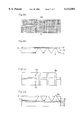
- FIG. 1 shows an optical coupler of an embodiment of the present invention
- FIG. 1 (a) is a plan view of the optical coupler P1
- FIG. 1 (b) is a side view of it.
- FIG. 2 shows the production steps of the optical coupler P1
- FIG. 2 (a) is a plan view of the optical coupler P1
- FIG. 2 (b) is a side view of it.
- FIG. 3 shows the production steps of the optical coupler P1
- FIG. 3 (a) is a plan view of the optical coupler P1
- FIG. 3 (b) is a side view of it.
- FIG. 4 shows the production steps of the optical coupler P1
- FIG. 4 (a) is a plan view of the optical coupler P1
- FIG. 4 (b) is a side view of it.
- FIG. 5 is a perspective view of an optical coupler P2 according to an embodiment of the present invention.
- FIG. 6 shows method of bonding the substrate and the optical element of the optical coupler P2
- FIG. 6 (a) is a side view showing the state before bonding
- FIG. 6 (b) is a side view at the time of rough alignment
- FIG. 6 (c) is a side view at the time of fine alignment.
- FIG. 7 is a perspective view of a conventional optical coupler P.
- FIG. 1 (a) is a plan view of an optical coupler P1
- FIG. 1 (b) is a side view of it.
- FIG. 2 through FIG. 4 show production steps of the optical coupler P1, and in each set of diagrams, (a) is a plan view of the optical coupler P1, and (b) is a side view of it.
- FIG. 5 is a perspective view of an optical coupler P2 of an embodiment
- FIGS. 6 (a) through (c) are side views illustrating the method of bonding a substrate and a optical element of the optical coupler P2 through the use of the self-alignment effect of solder.
- 1 denotes a substrate, and in one of its principal faces is formed a V-groove 4 for mounting an optical fiber.
- 3 is a thin film of Cr/Au, that is provided on a surface of the block 1a to be bonded with a base substrate 8. The thin film 3 has a good wettability with solder.
- 4 is the V-groove for mounting an optical fiber.
- 6 is a gap that is present between blocks 1a that are formed by dividing the substrate 1 into plural parts. 6a is a slit that is formed above the gap 6.
- 7 is a solder such as Au/Sn solder.
- 8 is the base substrate.
- 9 is an optical fiber
- 10 is an optical element such as an LN optical waveguide element.
- M denotes a marker that is formed by, for example, a metal film. These markers are formed on both the lower face of the optical element 10 and the upper face of the substrate 1. Two markers that are formed on the optical element 10 and two markers that are formed on the substrate 1 are aligned with each other, by using a light beam that penetrates through the optical element, to make visual alignment.
- the material for the substrate 1 is selected from crystal materials such as Si that is suited to fine working, plastics, and ceramics that have excellent thermal conductivity.
- the single crystal of Si is particularly preferred.
- the base substrate 8 is designed to have a coefficient of thermal expansion that is substantially identical to that of the optical element 10. The difference between the two should be, for example, within 20%. If the material of the base substrate 8 is identical to that of the optical element 10, they have the same coefficient of thermal expansion, however, there is no need of using the same material.
- Preferred materials for the base substrate 8 include LN, single crystal of lithium tantalate (LT), single crystal of lithium tetraborate (LBO), crystals of oxides such as KH2PO4 (KDP), glasses such as BK7 glass (trade name of HOYA Ltd.) and quartz glass, and semiconductors of Si, GaAs, InP, etc. These materials are the same materials that are used for the optical element 10 being an optical waveguide element, semiconductor optical waveguide element or semiconductor light emitting element such as LD and LED, or these materials have coefficients of thermal expansion that are substantially identical to that of the optical element 10.
- the coefficient of thermal expansion of the base substrate 8 may differ from that of the optical element 10 by about ⁇ 20%.
- the coefficient of thermal expansion of the substrate 1 is A
- the coefficient of thermal expansion of the optical element is within a range of from 0.8A to 1.2A, their coefficients of thermal expansion are regarded as substantially identical ones.
- the V-groove 4 is easily formed by anisotropic etching, etc., and the optical fiber 9 is stably mounted in the V-groove.
- the section of the groove may be concave, semi-circular, as well as V-shaped.
- the V-groove 4 may be formed by anisotropic etching with KOH, dry etching such as reactive ion etching, photolithography, mechanical cutting, etc.
- the optical element 10 may be an optical waveguide element, semiconductor optical waveguide element, semiconductor light emitting element such as LD and LED, or semiconductor light receiving element such as PD.
- the optical element 10 may be provided with electrodes for signal input or with electrodes for inputting electric field, magnetic field, sound, elastic surface wave, etc. to modulate the light.
- the blocks 1a of the optical coupler P1 can be formed from the substrate 1, like the V-groove 4, by anisotropic etching with KOH, etc.
- optical coupler P1 of the embodiment The production method of the optical coupler P1 of the embodiment will be described through the following steps (1) through (6).
- a second mask 3 for forming blocks 1a is formed, as shown in FIG. 2, by lift-off on the other principal face (the back and the face opposite to the face in which the V-groove 4 is formed) of the substrate 1 of single crystal of Si.
- the material of the second mask 3 is Cr/Au thin film that can resist anisotropic etching. This Cr/Au thin film also serves to wet the solder 7 when the base substrate 8 and the substrate 1 are bonded with solder later.
- the accuracy of the mask pattern formation about 10 ⁇ m is sufficient. Positional accuracy of this level can be achieved by simple alignment based on the orientation flat of the substrate 1.
- the width of the bottom of the block 1a in the longitudinal direction of the base substrate 8 is desired to be about 1 mm or less. This is to reduce any strains that may arise due to a difference in coefficient of thermal expansion between them. The reason is as follows:
- the coefficient of thermal expansion of LN that is the material of the base substrate 8 is 15.4 ⁇ 10 -6 (axis a of crystal) and 7.5 ⁇ 10 -6 (axis c of crystal).
- the coefficient of thermal expansion of Si that is the material of the substrate 1 is 2.6 ⁇ 10 -6 .
- the width of the block 1a in the longitudinal direction of the base substrate 1 is set at 1 mm or under, and preferably, the width of the block 1a in both the longitudinal and transverse directions is set at 1 mm or under.
- a film of a dielectric such as silicon nitride is formed as the first mask 2 that is for forming the V-groove 4 and also for etch stopping of the slit 6a.
- a pattern for forming the V-groove 4 is formed in the first mask 2 by etching. At this time, patterns for positioning the substrate 1 relative to the optical element 10 may be formed on the first mask 2.
- both the top and the back of the substrate 1 are subjected to anisotropic etching to form the V-groove 4 on the top of the substrate 1 and gaps 6 on the back of the substrate 1, gaps 6 reaching the top side thereof.
- etching of the gaps 6 is stopped by the first mask 2 that is formed on the top, and the slit 6a are formed on the top side of the substrate 1.
- anisotropic etching is done as follows.
- Anisotropic wet etching uses the fact that, when an alkaline etchant is used, the etch rate of the single crystal of Si depends significantly on the direction in the crystal. With this anisotropic wet etching, V-grooves and inverted trapezoidal grooves is formed on the surface of a substrate by precisely controlling the width and depth.
- Preferred alkaline etchants include KOH, NaOH, EPW (ethylenediamine+pyrocatechol+water), hydrazine, and TMAH (tetra-methyl-ammonium hydroxide).
- the etch rate of these alkaline etchants for the crystal plane (100) or (110) of Si single crystal is about several ten times through several hundred times as large as the etch rate for the crystal plane (111).
- the crystal planes of the substrate 1 are selected in such a way that the plane (111) for which the etch rate is small constitutes a side of the groove, fine working can be done with less undercut under the mask.
- the etch rate ratio of KOH is as large as several hundred times, and is most suited for fine working.
- the crystal plane (100) is selected as the top of the substrate 1, and the edges of the mask opening are straight lines parallel to or perpendicular to the direction (011). Then the V-groove 4 and the gaps 6 are formed by anisotropic wet etching. Their sides are crystal planes (111) that incline at an angle of 54.74° with the top of the substrate 1. Accordingly, the mask pattern is correctly reflected in the sides of the V-groove 4, etc., and when an optical device such as an optical fiber is held by these sides, a positioning accuracy comparable to that of the mask will be achieved.
- the depth of the V-groove 4 that is formed in the top of the substrate 1 and the selection between the V-groove 4 and an inverted trapezoidal groove are controlled by the etching time.
- the V-groove 4, etc. that are formed by such anisotropic wet etching have a positioning accuracy of, for example, ⁇ 0.5 ⁇ m or under.
- the markers M are covered by the first mask.
- the base substrate 8 is bonded onto the back of the substrate 1. It is bonded and fixed by reflow fixation, heating in an oven, or heating on a hot plate, then the first mask 2 is removed.
- the steps up to this point are effected by the conventional wafer processes.
- the conformed substrate, comprising the substrate 1 and the base substrate 8, can be produced in a large quantity by dicing wafers.
- gaps 6 and slits 6a can be formed without damaging the bonding face of the base substrate 8. Furthermore, through a method just like one mentioned above, a part of the back of the substrate 1 may be etched to form a high frequency wave transmission line or the like, that uses the air layer between the substrate 1 and the base substrate 8.
- the optical element 10 is mounted on the portion for mounting the optical element 10 on the substrate 1 in such a way that the optical waveguide edge (light emitting part or light receiving part) of the optical element 10 is optically connected to the optical fiber 9 that is to be mounted in the V-groove 4, then the solder 7 is heated and melted, and positional adjustment is made through the use of the self-alignment effect of the solder 7, and the optical element 10 is bonded onto the substrate 1.
- the optical fiber 9 is mounted in the V-groove 4, and the light beam incident end or light beam emergence end of the optical fiber 9 is butted and fixed against the optical waveguide edge (light emitting part or light receiving part) of the optical element 10 to complete optical connection between the optical element 10 and the optical fiber 9.
- Jointing of the optical element 10 and the substrate 1 may be effected without using the self-alignment effect of the solder 7. It may be effected by the visual alignment method. However, the self-alignment method is preferred. In this case, any apparatus for position detection such as a CCD camera is not required.
- the substrate 1 may be cut by the dicing method, etc., and blocks 1a may be bonded, one by one, onto the substrate 1.
- the method of the embodiment has excellent effects that blocks 1a can be directly formed from the substrate 1 and the blocks 1a can be bonded without disturbing the formation thereof. Bonding of the blocks 1a may be effected with an adhesive other than the solder 7.
- 22 denotes a base substrate of LN, etc.
- 11 is an optical element such as LN optical waveguide element.
- 12 is a substrate, a V-groove 13 for mounting an optical fiber is formed in one principal face of the substrate 12, and the substrate 12 is bonded onto the base substrate 22.
- 14a, 14b ⁇ 17a, 17b are plural trapezoidal (terrace-like) convexes formed in the portion for mounting the optical element of the substrate 12.
- a solder bump 18 is formed on each of these convexes 14a, 14b ⁇ 17a, 17b.
- Longitudinal slits 12a and transverse slits 12b are formed in the substrate 12 by dicing after jointing with the base substrate 22.
- the kinds of the optical element 11 and the materials of the substrate 12 are identical to those of the above-mentioned embodiment, and the method of forming the V-groove 12 is identical to that of the above-mentioned embodiment.
- the convexes 14a, 14b ⁇ 17a, 17b are formed by forming a layer of an electric insulator such as SiO2 of about 10 ⁇ m thick on the substrate 12, and after the formation of the V-groove 13, etching said insulator layer to pieces of several hundred ⁇ m wide and about 10 ⁇ m thick.
- an insulator as the material for the convexes 14a, 14b ⁇ 17a, 14b as mentioned above, and this prevents adverse effects on the electrodes, etc. of the optical element.
- the convexes 14a, 14b ⁇ 17a, 17b symmetrically about an extension of the V-groove 13, and to space them at substantially regular intervals along the extension of the V-groove 13.
- the convexes are also arranged in the periphery of the connecting face of the optical element 11 and an optical fiber not illustrated and near the V-groove 13. Or they may be arranged to pinch the V-groove 13 in between. With such an arrangement, satisfactory bonding strength and positioning accuracy can be obtained.
- the V-groove 13 extends up to the bonding face. However, the V-groove 13 may not be present in the bonding face.
- the melting temperature TL of the solders that are formed on the convexes 15a, 15b, 16a, 16b of lower height lower than the melting temperature TH of the solders that are formed on the convexes 14a, 14b, 17a, 17b of the higher height.
- FIG. 6 shows its bonding method.
- metal films (including alloy films) 24b ⁇ 27b such as Al thin film and Cr/Au thin film that have good wettability with solder, are provided in positions corresponding to the convexes 14a, 14b ⁇ 17a, 17b.
- metal films 24b, 25b, 26b, 27b, that correspond to the convexes 14b, 15b, 16b, 17b are illustrated.
- FIG. 6 (a) shows the state before bonding.
- the optical element 11 is placed on the substrate 12, but the position of the optical element 11 is slightly off the point.
- the optical element 11 is placed on the substrate 12 and the assembly is heated.
- the metal films 25a, 25b, 26a, 26b contact the solder bumps 18 on the convexes 15a, 15b, 16a, 16b.
- the temperature reaches TL
- the solders on the convexes 15a, 15b, 16a, 16b will melt first.
- the optical element 11 will be shifted horizontally and restored to its proper position; thus rough alignment is made. This is because the solder bumps 18 on the convexes 15a, 15b, 16a, 16b are larger, and their restoring forces are greater than those of smaller solder bumps but their positioning accuracy is inferior.
- the above-mentioned heating and solidification of the solders can be effected by well-known methods such as heating in an oven, beating on a hot plate, and reflow fixation.
- the optical element 11 will gradually descend of its own weight, and the metal films 24a, 24b, 27a, 27b will contact the solder bumps 18 on the convexes 14a, 14b, 17a, 17b.
- the temperature reaches TH, as shown in FIG. 6 (c)
- the solders on the convexes 14a, 14b, 17a, 17b will be melted.
- fine alignment in the horizontal direction and fine adjustment in the direction of height is effected. This is because the solder bumps 18 on the convexes 14a, 14b, 17a, 17b are small, and their restoring forces are small but the resulting positioning accuracy is high.
- positioning in one direction is illustrated, but positioning can be made two-dimensionally in a plane.
- the difference in melting temperature of solder within a range of from about 0.1° C. to about 10° C. If the difference is less than 0.1° C., all the solders will melt quickly one after another, making it hard to have a proper interval; thus it will be difficult to effect stepwise adjustment. On the other hand, if the difference is greater than 10° C., said interval will get longer, and new displacement may be caused by external vibration, etc., or the solders that melt first may solidify before the next solders melt; it tends to make adjustment impracticable.
- the diameters are less than 100 ⁇ m, the shift of the optical element 11 due to the self-alignment effect of the solders will be small and it will be hard to make rough alignment, and if the diameters exceed 200 ⁇ m, the shift of the optical element 11 will be large, and the accuracy of rough alignment will deteriorate.
- the difference in height of the convexes 14a, 14b ⁇ 17a, 17b corresponds to the diameter of the solder bumps 18 on the convexes 15a, 15b, 16a, 16b, and it is desirable to keep the difference a little smaller than that diameter or within a range of from about 50 ⁇ m to about 100 ⁇ m. If the difference in height is less than 50 ⁇ m, the shift of the optical element 11 due to the self-alignment effect of the solder is small and it is difficult to make alignment. If the difference exceeds 100 ⁇ m, the shift of the optical element 11 will get larger and the accuracy of alignment will deteriorate.
- bonding of the substrate and the optical element that is to be mounted on the substrate is effected by simple steps, that use the self-alignment effect of solders, with high positioning accuracy, and even when the substrate and the optical element differ in coefficient of thermal expansion from each other, stresses and strains, that are generated in the substrate during bonding and after bonding of the substrate and the optical element, are moderated to effectively prevent fluctuations of the positioning accuracy of the optical connection.
- slits 12b, etc. may be omitted.
- the present invention is not limited to the respective embodiments, and various modifications can be made within a range that does not deviate from the gist of the present invention.
Applications Claiming Priority (2)
| Application Number | Priority Date | Filing Date | Title |
|---|---|---|---|
| JP20501897A JP3792358B2 (ja) | 1997-07-30 | 1997-07-30 | 光接続部品及びその製造方法 |
| JP9-205018 | 1997-07-30 |
Publications (1)
| Publication Number | Publication Date |
|---|---|
| US6112001A true US6112001A (en) | 2000-08-29 |
Family
ID=16500088
Family Applications (1)
| Application Number | Title | Priority Date | Filing Date |
|---|---|---|---|
| US09/124,403 Expired - Fee Related US6112001A (en) | 1997-07-30 | 1998-07-29 | Optical coupler and a method of producing it |
Country Status (4)
| Country | Link |
|---|---|
| US (1) | US6112001A (ja) |
| JP (1) | JP3792358B2 (ja) |
| GB (1) | GB2329486B (ja) |
| IT (1) | IT1302415B1 (ja) |
Cited By (30)
| Publication number | Priority date | Publication date | Assignee | Title |
|---|---|---|---|---|
| WO2001022785A1 (en) * | 1999-09-20 | 2001-03-29 | Nas Interplex Industries Inc. | Solder-bearing wafer for use in soldering operations |
| US6256437B1 (en) * | 1997-09-30 | 2001-07-03 | Kyocera Corporation | Optical device and its production method |
| US20020029975A1 (en) * | 2000-08-01 | 2002-03-14 | Westra Kenneth Lloyd | Method of making a high reflectivity micro mirror and a micro mirror |
| US6443631B1 (en) | 2001-02-20 | 2002-09-03 | Avanti Optics Corporation | Optical module with solder bond |
| US20020168147A1 (en) * | 2001-02-20 | 2002-11-14 | Case Steven K. | Optical circuit pick and place machine |
| US6519394B2 (en) * | 2000-03-01 | 2003-02-11 | Ngk Insulators, Ltd. | Bonding structure of optical members |
| US6546173B2 (en) | 2001-02-20 | 2003-04-08 | Avanti Optics Corporation | Optical module |
| US6546172B2 (en) | 2001-02-20 | 2003-04-08 | Avanti Optics Corporation | Optical device |
| US6543114B2 (en) * | 2001-03-08 | 2003-04-08 | Axsun Technologies, Inc. | Manufacturing system using solder self-alignment with optical component deformation fine alignment |
| WO2003035269A1 (en) | 2001-10-24 | 2003-05-01 | Willem Brinkhuis | Process, system and equipment for the application of coatings onto walls of tunnels, pipes, tubes and the like |
| US20030223693A1 (en) * | 2002-06-04 | 2003-12-04 | Tallent Jack R. | Fiber optic device with enhanced resistance to environmental conditions and method |
| US20040022488A1 (en) * | 2002-07-31 | 2004-02-05 | Coleman Christopher L. | Optical fiber coupler having a relaxed alignment tolerance |
| US20040033023A1 (en) * | 2002-06-04 | 2004-02-19 | Tallent Jack R. | Fiber optic device with enhanced resistance to environmental conditions and method |
| US20040042729A1 (en) * | 2002-08-28 | 2004-03-04 | Phosistor Technologies, Inc. | Optical beam transformer module for light coupling between a fiber array and a photonic chip and the method of making the same |
| US20040062484A1 (en) * | 2002-08-29 | 2004-04-01 | International Business Machines Corporation | Self-aligned optical waveguide to optical fiber connection system |
| US6804770B2 (en) | 2001-03-22 | 2004-10-12 | International Business Machines Corporation | Method and apparatus for using past history to avoid flush conditions in a microprocessor |
| US20040212802A1 (en) * | 2001-02-20 | 2004-10-28 | Case Steven K. | Optical device with alignment compensation |
| US20040264870A1 (en) * | 2002-08-20 | 2004-12-30 | Skunes Timothy A. | Optical alignment mount with height adjustment |
| US20050036738A1 (en) * | 2002-08-28 | 2005-02-17 | Phosistor Technologies, Inc. | Varying refractive index optical medium using at least two materials with thicknesses less than a wavelength |
| US6879757B1 (en) | 2001-12-11 | 2005-04-12 | Phosistor Technologies, Inc. | Connection between a waveguide array and a fiber array |
| US6888989B1 (en) | 2001-12-11 | 2005-05-03 | Phosistor Technologies, Inc. | Photonic chip mounting in a recess for waveguide alignment and connection |
| US6900393B1 (en) | 1999-09-20 | 2005-05-31 | Teka Interconnections Systems, Inc. | Solder-bearing wafer for use in soldering operations |
| US20050220415A1 (en) * | 2004-03-31 | 2005-10-06 | Imra America, Inc. | Etched plate alignment method and apparatus |
| US6956999B2 (en) | 2001-02-20 | 2005-10-18 | Cyberoptics Corporation | Optical device |
| US20070152018A1 (en) * | 1999-09-20 | 2007-07-05 | Interplex Nas, Inc. | Solder-bearing wafer for use in soldering operations |
| AU2003264988B2 (en) * | 2002-10-02 | 2009-12-03 | Lg Electronics Inc. | Recording medium having a data structure for managing reproduction of graphic data and recording and reproducing methods and apparatuses |
| US20100135615A1 (en) * | 2002-08-28 | 2010-06-03 | Seng-Tiong Ho | Apparatus for coupling light between input and output waveguides |
| CN101299082B (zh) * | 2007-02-14 | 2012-02-29 | 日本电气株式会社 | 光学模块 |
| US20140348463A1 (en) * | 2011-10-04 | 2014-11-27 | Citizen Holdings Co., Ltd. | Optical device and method for manufacuturing the optical device |
| US20160154179A1 (en) * | 2013-07-24 | 2016-06-02 | Effect Photonics B.V. | Optical subassembly, optical system and method |
Families Citing this family (2)
| Publication number | Priority date | Publication date | Assignee | Title |
|---|---|---|---|---|
| CN1433527A (zh) * | 1999-12-24 | 2003-07-30 | 康宁Oti股份公司 | 有源器件的组件 |
| US6614966B2 (en) | 2000-03-22 | 2003-09-02 | Matsushita Electric Industrial Co., Ltd. | Optical waveguide device integrated module and method of manufacturing the same |
Citations (2)
| Publication number | Priority date | Publication date | Assignee | Title |
|---|---|---|---|---|
| US4892377A (en) * | 1987-08-19 | 1990-01-09 | Plessey Overseas Limited | Alignment of fibre arrays |
| EP0588675A1 (fr) * | 1992-08-14 | 1994-03-23 | Commissariat A L'energie Atomique | Procédé d'hybridation et de positionnement d'un composant optoélectronique par rapport à un guide optique intégré |
-
1997
- 1997-07-30 JP JP20501897A patent/JP3792358B2/ja not_active Expired - Fee Related
-
1998
- 1998-07-29 US US09/124,403 patent/US6112001A/en not_active Expired - Fee Related
- 1998-07-30 GB GB9816643A patent/GB2329486B/en not_active Expired - Fee Related
- 1998-07-30 IT IT1998RM000510A patent/IT1302415B1/it active IP Right Grant
Patent Citations (3)
| Publication number | Priority date | Publication date | Assignee | Title |
|---|---|---|---|---|
| US4892377A (en) * | 1987-08-19 | 1990-01-09 | Plessey Overseas Limited | Alignment of fibre arrays |
| EP0588675A1 (fr) * | 1992-08-14 | 1994-03-23 | Commissariat A L'energie Atomique | Procédé d'hybridation et de positionnement d'un composant optoélectronique par rapport à un guide optique intégré |
| US5321786A (en) * | 1992-08-14 | 1994-06-14 | Commissariat A L'energie Atomique | Process for the hybridization and positioning of an optoelectronic component relative to an integrated optical guide |
Non-Patent Citations (2)
| Title |
|---|
| Wale, et al. "Self-Aligned Flip-Chip Assembly of Photonic Devices with Electrical and Optical Connections," IEEE Transactions on Components, Hybrids, and Manufacturing Technology, vol. 13, No. 4, Dec. 1990, pp. 780-786. |
| Wale, et al. Self Aligned Flip Chip Assembly of Photonic Devices with Electrical and Optical Connections, IEEE Transactions on Components, Hybrids, and Manufacturing Technology, vol. 13, No. 4, Dec. 1990, pp. 780 786. * |
Cited By (56)
| Publication number | Priority date | Publication date | Assignee | Title |
|---|---|---|---|---|
| US6256437B1 (en) * | 1997-09-30 | 2001-07-03 | Kyocera Corporation | Optical device and its production method |
| GB2372154B (en) * | 1999-09-20 | 2003-09-24 | Nas Interplex Ind Inc | Solder-bearing wafer for use in soldering operations |
| US6900393B1 (en) | 1999-09-20 | 2005-05-31 | Teka Interconnections Systems, Inc. | Solder-bearing wafer for use in soldering operations |
| GB2372154A (en) * | 1999-09-20 | 2002-08-14 | Nas Interplex Ind Inc | Solder-bearing wafer for use in soldering operations |
| US20060090932A1 (en) * | 1999-09-20 | 2006-05-04 | Cachina Joseph S | Solder-bearing wafer for use in soldering operations |
| US20070152018A1 (en) * | 1999-09-20 | 2007-07-05 | Interplex Nas, Inc. | Solder-bearing wafer for use in soldering operations |
| WO2001022785A1 (en) * | 1999-09-20 | 2001-03-29 | Nas Interplex Industries Inc. | Solder-bearing wafer for use in soldering operations |
| US7259335B2 (en) | 1999-09-20 | 2007-08-21 | Teka Interconnections Systems, Inc. | Solder-bearing wafer for use in soldering operations |
| US7754979B2 (en) | 1999-09-20 | 2010-07-13 | Teka Interconnections Systems, Inc. | Solder-bearing wafer for use in soldering operations |
| US6519394B2 (en) * | 2000-03-01 | 2003-02-11 | Ngk Insulators, Ltd. | Bonding structure of optical members |
| US7016128B2 (en) | 2000-08-01 | 2006-03-21 | Kenneth Lloyd Westra | Method of making a high reflectivity micro mirror and a micro mirror |
| US20020029975A1 (en) * | 2000-08-01 | 2002-03-14 | Westra Kenneth Lloyd | Method of making a high reflectivity micro mirror and a micro mirror |
| US20050032377A1 (en) * | 2000-08-01 | 2005-02-10 | Westra Kenneth Lloyd | Movable optical element assembly with highly reflective surface |
| US6546172B2 (en) | 2001-02-20 | 2003-04-08 | Avanti Optics Corporation | Optical device |
| US20050249464A1 (en) * | 2001-02-20 | 2005-11-10 | Case Steven K | Optical device with alignment compensation |
| US6546173B2 (en) | 2001-02-20 | 2003-04-08 | Avanti Optics Corporation | Optical module |
| US20020168147A1 (en) * | 2001-02-20 | 2002-11-14 | Case Steven K. | Optical circuit pick and place machine |
| US6443631B1 (en) | 2001-02-20 | 2002-09-03 | Avanti Optics Corporation | Optical module with solder bond |
| US20030219210A1 (en) * | 2001-02-20 | 2003-11-27 | Case Steven K. | Optical module |
| US7010855B2 (en) | 2001-02-20 | 2006-03-14 | Cyberoptics Corporation | Optical module |
| US6956999B2 (en) | 2001-02-20 | 2005-10-18 | Cyberoptics Corporation | Optical device |
| US20040212802A1 (en) * | 2001-02-20 | 2004-10-28 | Case Steven K. | Optical device with alignment compensation |
| US6971164B2 (en) | 2001-02-20 | 2005-12-06 | Cyberoptics Corporation | Optical device |
| US6543114B2 (en) * | 2001-03-08 | 2003-04-08 | Axsun Technologies, Inc. | Manufacturing system using solder self-alignment with optical component deformation fine alignment |
| US20030162003A1 (en) * | 2001-03-08 | 2003-08-28 | Axsun Technologies, Inc. | Manufacturing system using solder self-alignment with optical component deformation fine alignment |
| US6804770B2 (en) | 2001-03-22 | 2004-10-12 | International Business Machines Corporation | Method and apparatus for using past history to avoid flush conditions in a microprocessor |
| WO2003035269A1 (en) | 2001-10-24 | 2003-05-01 | Willem Brinkhuis | Process, system and equipment for the application of coatings onto walls of tunnels, pipes, tubes and the like |
| US6879757B1 (en) | 2001-12-11 | 2005-04-12 | Phosistor Technologies, Inc. | Connection between a waveguide array and a fiber array |
| US6888989B1 (en) | 2001-12-11 | 2005-05-03 | Phosistor Technologies, Inc. | Photonic chip mounting in a recess for waveguide alignment and connection |
| US6865322B2 (en) | 2002-06-04 | 2005-03-08 | Goi Acquisitions Llc | Fiber optic device with enhanced resistance to environmental conditions and method |
| US20030223693A1 (en) * | 2002-06-04 | 2003-12-04 | Tallent Jack R. | Fiber optic device with enhanced resistance to environmental conditions and method |
| US6741774B2 (en) | 2002-06-04 | 2004-05-25 | Gould Fiber Optics, Inc. | Fiber optic device with enhanced resistance to environmental conditions and method |
| US20040033023A1 (en) * | 2002-06-04 | 2004-02-19 | Tallent Jack R. | Fiber optic device with enhanced resistance to environmental conditions and method |
| DE10320152B4 (de) * | 2002-07-31 | 2006-07-13 | Agilent Technologies, Inc. (n.d.Ges.d.Staates Delaware), Palo Alto | Optikfaserkoppler mit erweiterter Ausrichtungstoleranz |
| US6956992B2 (en) | 2002-07-31 | 2005-10-18 | Agilent Technologies, Inc. | Optical fiber coupler having a relaxed alignment tolerance |
| US20050259918A1 (en) * | 2002-07-31 | 2005-11-24 | Coleman Christopher L | Optical fiber coupler having a relaxed alignment tolerance |
| US7308170B2 (en) | 2002-07-31 | 2007-12-11 | Avago Technologies Fiber Ip (Singapore) Pte Ltd | Optical fiber coupler having a relaxed alignment tolerance |
| US20040022488A1 (en) * | 2002-07-31 | 2004-02-05 | Coleman Christopher L. | Optical fiber coupler having a relaxed alignment tolerance |
| US20040264870A1 (en) * | 2002-08-20 | 2004-12-30 | Skunes Timothy A. | Optical alignment mount with height adjustment |
| US20100135615A1 (en) * | 2002-08-28 | 2010-06-03 | Seng-Tiong Ho | Apparatus for coupling light between input and output waveguides |
| US7616856B2 (en) | 2002-08-28 | 2009-11-10 | Phosistor Technologies, Inc. | Varying refractive index optical medium using at least two materials with thicknesses less than a wavelength |
| US20040042729A1 (en) * | 2002-08-28 | 2004-03-04 | Phosistor Technologies, Inc. | Optical beam transformer module for light coupling between a fiber array and a photonic chip and the method of making the same |
| US8538208B2 (en) | 2002-08-28 | 2013-09-17 | Seng-Tiong Ho | Apparatus for coupling light between input and output waveguides |
| US7303339B2 (en) | 2002-08-28 | 2007-12-04 | Phosistor Technologies, Inc. | Optical beam transformer module for light coupling between a fiber array and a photonic chip and the method of making the same |
| US20050036738A1 (en) * | 2002-08-28 | 2005-02-17 | Phosistor Technologies, Inc. | Varying refractive index optical medium using at least two materials with thicknesses less than a wavelength |
| US7426328B2 (en) | 2002-08-28 | 2008-09-16 | Phosistor Technologies, Inc. | Varying refractive index optical medium using at least two materials with thicknesses less than a wavelength |
| US20090046979A1 (en) * | 2002-08-28 | 2009-02-19 | Phosistor Technologies, Inc. | Varying refractive index optical medium using at least two materials with thicknesses less than a wavelength |
| US6819841B2 (en) | 2002-08-29 | 2004-11-16 | International Business Machines Corporation | Self-aligned optical waveguide to optical fiber connection system |
| US20040062484A1 (en) * | 2002-08-29 | 2004-04-01 | International Business Machines Corporation | Self-aligned optical waveguide to optical fiber connection system |
| AU2003264988B2 (en) * | 2002-10-02 | 2009-12-03 | Lg Electronics Inc. | Recording medium having a data structure for managing reproduction of graphic data and recording and reproducing methods and apparatuses |
| US7146083B2 (en) | 2004-03-31 | 2006-12-05 | Imra America, Inc. | Etched plate alignment method and apparatus |
| US20050220415A1 (en) * | 2004-03-31 | 2005-10-06 | Imra America, Inc. | Etched plate alignment method and apparatus |
| CN101299082B (zh) * | 2007-02-14 | 2012-02-29 | 日本电气株式会社 | 光学模块 |
| US20140348463A1 (en) * | 2011-10-04 | 2014-11-27 | Citizen Holdings Co., Ltd. | Optical device and method for manufacuturing the optical device |
| US20160154179A1 (en) * | 2013-07-24 | 2016-06-02 | Effect Photonics B.V. | Optical subassembly, optical system and method |
| US9488785B2 (en) * | 2013-07-24 | 2016-11-08 | Effect Photonics B.V. | Optical subassembly, optical system and method |
Also Published As
| Publication number | Publication date |
|---|---|
| ITRM980510A0 (it) | 1998-07-30 |
| GB9816643D0 (en) | 1998-09-30 |
| JPH1152190A (ja) | 1999-02-26 |
| GB2329486B (en) | 2002-01-16 |
| IT1302415B1 (it) | 2000-09-05 |
| ITRM980510A1 (it) | 2000-01-30 |
| JP3792358B2 (ja) | 2006-07-05 |
| GB2329486A (en) | 1999-03-24 |
Similar Documents
| Publication | Publication Date | Title |
|---|---|---|
| US6112001A (en) | Optical coupler and a method of producing it | |
| EP0283301B1 (en) | Connecting optical fibers | |
| US6118917A (en) | Optical fiber passive alignment apparatus using alignment platform | |
| US5787214A (en) | Connection between an integrated optical waveguide and an optical fibre | |
| KR100302144B1 (ko) | 실리콘온인슐레이터 광도파로를 이용한 커넥터형 광트랜시버 | |
| EP0541386A1 (en) | Optical interconnection circuit structure | |
| EP0466134A2 (en) | Method and device for passive alignment of diode lasers and optical fibers | |
| JPH07249798A (ja) | 光部品固定装置及びその製造方法 | |
| CA2128534C (en) | Alignment of integrated optical components | |
| JP2924953B2 (ja) | 光素子の実装構造 | |
| US5548673A (en) | Optical coupling device | |
| JPH08204288A (ja) | 光半導体装置 | |
| CN215067594U (zh) | 光波导元件 | |
| JP2823044B2 (ja) | 光結合回路及びその製造方法 | |
| US5535295A (en) | Coupling structure for waveguide connection and process of forming the same | |
| JP2862625B2 (ja) | 埋め込み型石英系光導波路およびその製造方法 | |
| US6847764B2 (en) | Optical interconnect having alignment depression | |
| EP0846966A2 (en) | Optical waveguide | |
| US20030235388A1 (en) | Method for fabricating fiber blocks using solder as bonding material | |
| WO2002075387A2 (en) | A tapered optical waveguide | |
| KR100211039B1 (ko) | 광스위치-광섬유 광결합 장치 | |
| JPH0527140A (ja) | 光伝送装置およびその製造方法 | |
| JPH04358105A (ja) | 光平面導波路と光ファイバの接続構造 | |
| JP3761051B2 (ja) | 光半導体結合装置の製造方法 | |
| KR100271826B1 (ko) | 레이저 다이오드 칩과 광 파이버의 정열방법 |
Legal Events
| Date | Code | Title | Description |
|---|---|---|---|
| AS | Assignment |
Owner name: KYOCERA CORPORATION, JAPAN Free format text: ASSIGNMENT OF ASSIGNORS INTEREST;ASSIGNORS:KISHIDA, YUJI;KOMEDA, RYUJI;KUBA, YUTAKA;AND OTHERS;REEL/FRAME:009361/0106 Effective date: 19980721 |
|
| FPAY | Fee payment |
Year of fee payment: 4 |
|
| FPAY | Fee payment |
Year of fee payment: 8 |
|
| REMI | Maintenance fee reminder mailed | ||
| LAPS | Lapse for failure to pay maintenance fees | ||
| STCH | Information on status: patent discontinuation |
Free format text: PATENT EXPIRED DUE TO NONPAYMENT OF MAINTENANCE FEES UNDER 37 CFR 1.362 |
|
| FP | Lapsed due to failure to pay maintenance fee |
Effective date: 20120829 |