US6104635A - Non-volatile memory device readable write data latch, and internal control thereof - Google Patents
Non-volatile memory device readable write data latch, and internal control thereof Download PDFInfo
- Publication number
- US6104635A US6104635A US09/143,447 US14344798A US6104635A US 6104635 A US6104635 A US 6104635A US 14344798 A US14344798 A US 14344798A US 6104635 A US6104635 A US 6104635A
- Authority
- US
- United States
- Prior art keywords
- data
- read
- memory cells
- memory device
- write
- Prior art date
- Legal status (The legal status is an assumption and is not a legal conclusion. Google has not performed a legal analysis and makes no representation as to the accuracy of the status listed.)
- Expired - Fee Related
Links
- 230000015654 memory Effects 0.000 claims abstract description 92
- 239000004065 semiconductor Substances 0.000 claims abstract description 27
- 230000006870 function Effects 0.000 claims abstract description 4
- 238000000034 method Methods 0.000 claims description 23
- 230000000295 complement effect Effects 0.000 claims description 17
- 230000005689 Fowler Nordheim tunneling Effects 0.000 claims description 12
- 230000004044 response Effects 0.000 claims description 3
- 238000010586 diagram Methods 0.000 description 12
- 239000000872 buffer Substances 0.000 description 8
- 238000003491 array Methods 0.000 description 4
- 230000003321 amplification Effects 0.000 description 3
- 239000002784 hot electron Substances 0.000 description 3
- 238000002347 injection Methods 0.000 description 3
- 239000007924 injection Substances 0.000 description 3
- 238000003199 nucleic acid amplification method Methods 0.000 description 3
- 239000000758 substrate Substances 0.000 description 3
- 230000004913 activation Effects 0.000 description 1
- 238000007796 conventional method Methods 0.000 description 1
- 230000001934 delay Effects 0.000 description 1
- 230000005641 tunneling Effects 0.000 description 1
Images


Classifications
-
- G—PHYSICS
- G11—INFORMATION STORAGE
- G11C—STATIC STORES
- G11C16/00—Erasable programmable read-only memories
- G11C16/02—Erasable programmable read-only memories electrically programmable
- G11C16/06—Auxiliary circuits, e.g. for writing into memory
- G11C16/26—Sensing or reading circuits; Data output circuits
-
- G—PHYSICS
- G11—INFORMATION STORAGE
- G11C—STATIC STORES
- G11C16/00—Erasable programmable read-only memories
- G11C16/02—Erasable programmable read-only memories electrically programmable
- G11C16/06—Auxiliary circuits, e.g. for writing into memory
- G11C16/10—Programming or data input circuits
-
- G—PHYSICS
- G11—INFORMATION STORAGE
- G11C—STATIC STORES
- G11C7/00—Arrangements for writing information into, or reading information out from, a digital store
- G11C7/10—Input/output [I/O] data interface arrangements, e.g. I/O data control circuits, I/O data buffers
- G11C7/1051—Data output circuits, e.g. read-out amplifiers, data output buffers, data output registers, data output level conversion circuits
-
- G—PHYSICS
- G11—INFORMATION STORAGE
- G11C—STATIC STORES
- G11C7/00—Arrangements for writing information into, or reading information out from, a digital store
- G11C7/10—Input/output [I/O] data interface arrangements, e.g. I/O data control circuits, I/O data buffers
- G11C7/1078—Data input circuits, e.g. write amplifiers, data input buffers, data input registers, data input level conversion circuits
Definitions
- the present invention relates to a non-volatile semiconductor memory device with a data latch that stores both read data and write data.
- Non-volatile read/write memory devices such as flash memory devices employ two methods, hot-electron injection and Fowler-Nordheim tunneling, to store and erase data in their memory cells.
- Fowler-Nordheim tunneling is the slower method, taking a few hundred to a few thousand microseconds to write data that could be written in a few tens of microseconds by hot-electron injection.
- Fowler-Nordheim tunneling is an attractive data-writing method because it draws very little current, enabling the necessary writing voltages to be generated within the memory device.
- the slowness of Fowler-Nordheim tunneling write operations can be hidden by providing each bit line in the memory device with a latch for holding write data.
- write data When write data have been stored in all of the latches, one word line is activated, and the data are written all at once into the memory cells coupled to the word line.
- the write cycle time becomes the time needed to store the data in the write latches, which is the same regardless of the method employed to write the data into the memory cells.
- the same latches are often made to function as sense amplifiers in data read operations. Read data from all memory cells coupled to a designated word line are sensed and amplified simultaneously by the latches. After sense amplification, the latches become a cache from which the read data can be accessed quickly, without further sense amplification, in a manner similar to fast page mode read access in a dynamic random-access memory (DRAM).
- DRAM dynamic random-access memory
- the invented semiconductor memory device has non-volatile memory cells, and one or more data latches for storing both write data to be written into the memory cells and read data read from the memory cells.
- a data polarity control circuit generates a selection signal indicating whether the data stored in the data latches are read data or write data.
- a data polarity switch generates externally readable data by outputting the data stored in the data latches when the selection signal indicates that read data are stored, and inverting the data stored in the data latches when the selection signal indicates that write data are stored.
- Write data are preferably stored in the memory cells by Fowler-Nordheim tunneling.
- the data latches preferably function as sense amplifiers when data are read from the memory cells.
- the selection signal is preferably reset when the memory device is powered up.
- the invented method of controlling the above semiconductor memory thus comprises the steps of:
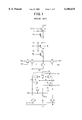
- FIG. 1 is a circuit diagram of a bit line and data latch in a conventional flash memory
- FIG. 2 is a waveform diagram illustrating the writing of data into a memory cell in FIG. 1;
- FIG. 3 is a waveform diagram illustrating the reading of data from a memory cell in FIG. 1;
- FIG. 4 is a block diagram of a flash memory device embodying the present invention.
- FIG. 5 is a circuit diagram showing a bit line, a data latch, and the input/output control unit in FIG. 4;
- FIG. 6 is a more detailed circuit diagram of the data line driver in FIG. 5;
- FIG. 7 is a more detailed circuit diagram of the data line amplifier in FIG. 5;
- FIG. 8 is a more detailed circuit diagram of the data polarity switch in FIG. 5;
- FIG. 9 is a more detailed circuit diagram of the data polarity control circuit in FIG. 5;
- FIG. 10 is a waveform diagram illustrating read and write operations in the flash memory device in FIG. 4.
- FIG. 11 is a block diagram of the input/output control unit in another flash memory device embodying the present invention.
- FIG. 1 shows one bit line 6 and associated circuitry in a flash memory device with a NOR memory-cell architecture, employing Fowler-Nordheim tunneling for writing data.
- the associated circuitry comprises transistors 1 to 5 and 7, two complementary data lines 8 and 9, and further transistors 10 to 18.
- Transistors 1 and 3 are p-channel metal-oxide-semiconductor (PMOS) transistors.
- the other transistors are n-channel metal-oxide-semiconductor (NMOS) transistors.
- Transistors 1, 2, 3, 4, and 16 constitute a data latch 19 that also operates as a sense amplifier.
- the source electrodes of transistors 1 and 3 are coupled to a power supply node VP.
- the source electrodes of transistors 2 and 4 are coupled to a ground node VN.
- the drain electrodes of transistors 1 and 2 and the gate electrodes of transistors 3 and 4 are coupled in common to a data node A.
- the drain electrodes of transistors 3 and 4 and the gate electrodes of transistors 1 and 2 are coupled in common to a complementary data node B.
- the gate electrodes of transistors 1 and 3 are mutually interconnected through transistor 16, the gate electrode of which receives an equalize signal EQ.
- Transistor 5 which constitutes a memory cell, has two gate electrodes, one coupled to a word line WL, the other floating.
- the source electrode of transistor 5 is coupled to a source line SL.
- the drain electrode of transistor 5 is coupled to bit line 6.
- Other memory cells are similarly coupled to bit line 6 and to respective word lines and source lines.
- the bit line 6 is coupled to node A of the data latch 19 through a transfer transistor 7, the gate electrode of which receives a transfer signal T.
- Node A is coupled through transistor 10 to data line 8, and node B through transistor 11 to data line 9.
- the gate electrodes of transistors 10 and 11 are controlled by a decoded address signal Y.
- a write potential Vd is supplied through transistors 12 and 13 to the end of bit line 6 near transfer transistor 7.
- Transistors 12 and 13 are coupled in series.
- the gate electrode of transistor 13 receives a write signal WR.
- the gate electrode of transistor 12 is coupled to node A.
- An initial potential or write inhibit potential Vi is supplied through transistor 14 to the end of bit line 6 distant from transfer transistor 7.
- the gate electrode of transistor 14 receives an initializing signal VINT.
- a read potential VRD is supplied through transistor 15 to the end of bit line 6 near transfer transistor 7.
- VRD is intermediate between Vcc and 1/2Vcc, where Vcc is a power-supply potential representing the binary ⁇ 1 ⁇ logic level or high logic level.
- the gate electrode of transistor 15 receives a read signal RD.
- a potential equal to 1/2Vcc is supplied to nodes A and B through transistors 17 and 18, respectively.
- the gate electrodes of transistors 17 and 18 receive the equalize signal EQ.
- the memory cell Before data are written into a memory cell 5, the memory cell is erased to the logic ⁇ 1 ⁇ state by applying voltages that cause electrons to tunnel into its floating gate.
- the negative charge thus stored in the floating gate raises the transistor on-off discrimination point of the memory cell 5 from a value V 0 (such as 1/2Vcc), which would obtain in the absence of a floating gate charge, to a higher value V 0 + ⁇ 1 , where ⁇ 1 is, for example, about half a volt.
- New data that will be written into a memory cell 5 are first stored in the data latch 19.
- the write data are placed on the complementary data lines 8 and 9. If a ⁇ 0 ⁇ is to be stored, data line 8 is driven to the high logic level (Vcc) and data line 9 to the low logic level or ground level (Vss). If a ⁇ 1 ⁇ is to be stored, data line 8 is driven to the low logic level (Vss), and data line 9 to the high logic level (Vcc).
- the address signal Y is placed at the high logic level, so that the node A is driven to the same potential as data line 8, and node B to the same potential as data line 9.
- node VP is driven to Vcc, and node VN is driven to Vss, so nodes A and B are held at their existing potential levels even after the address signal Y goes low.
- Node A thus remains high (Vcc) if the write data value is ⁇ 0, ⁇ and low (Vss) if the write value is ⁇ 1. ⁇
- the new data are stored in memory cell 5 by the procedure illustrated in FIG. 2.
- the write operation takes place during an interval defined by a master write signal (waveform z) generated by a control circuit not shown in FIG. 1.
- This control circuit also generates the above-mentioned VINT, WR, RD, EQ, and T signals, and controls the VP, VN, and word-line (WL) potentials. All of these signals and potentials are initially at the ground level (Vss) except for VP, which is initially at the high logic level (Vcc).
- the RD and EQ signals and VN potential remain at the ground level (waveforms c, d, and g), and the source line (SL, not shown in FIG. 2) of the memory cell 5 is left in the high-impedance state.
- VINT When the master write signal goes high, VINT is also driven to the active or high level (waveform a), briefly turning on transistor 14 and precharging bit line 6 (BL, waveform j) to the write inhibit potential Vi.
- VINT goes low, the WR and T signals (waveforms b and e) are first driven to the active or high level (Vcc); then WR, T, and VP (waveform f) are driven to a still higher voltage level equal to or greater than Vd+Vt, where Vt is the threshold voltage of transistors 7, 12, and 13.
- Vt is the threshold voltage of transistors 7, 12, and 13.
- a negative programming voltage VPG is applied to the word line (WL, waveform k)
- VP returns to the Vcc level
- WR and T return to the Vss level
- VINT is driven high again (waveform a) to precharge the bit line 6 to the Vi potential once more.
- FIG. 3 illustrates the operation of reading data from memory cell 5.
- the read operation is controlled by a master read signal (waveform z).
- Waveforms a-k designate the same signals as in FIG. 2.
- the source line (SL, not shown in FIG. 3) is held at the ground potential (Vss).
- VINT is driven to the active (high) level to precharge the bit line 6 to the initial Vi potential (waveforms a and j).
- the RD signal is driven to the active (high) level to supply the VRD potential to the bit line (waveforms c and j).
- VP and VN are both brought to 1/2Vcc and the equalize signal EQ is driven to the active (high) level, mutually short-circuiting nodes A and B through transistor 16, and supplying 1/2Vcc to nodes A and B through transistors 17 and 18 (waveforms d, f, g, h, and i).
- the word line (WL, waveform k) is driven to a read gate voltage VRG that is less than V 0 + ⁇ 1 but greater than V 0 - ⁇ 2 . If a ⁇ 1 ⁇ is stored in memory cell 5, then VRG is less than the on-off discrimination voltage (V 0 + ⁇ 1 ) of the memory cell, so its transistor remains turned off, and the bit line 6 remains at the VRD potential. If a ⁇ 0 ⁇ is stored in memory cell 5, however, then VRG exceeds the on-off discrimination voltage (V 0 - ⁇ 2 ), so the memory-cell transistor turns on, and the bit line 6 begins to discharge toward the ground level of the source line.
- the potential of the bit line (waveform k) will have discharged to a potential less than 1/2Vcc if the memory cell 5 holds a ⁇ 0, ⁇ but will still be at potential VRD, greater than 1/2Vcc, if the memory cell 5 holds a ⁇ 1.
- the equalize signal EQ is driven low and the transfer signal T is driven high (waveforms d and e), transferring the bit-line potential to node A, thus creating a potential difference between nodes A and B.
- signal T is driven low, VP is driven to Vcc, VN is driven to Vss (waveforms e, f, and g), and the potential difference between nodes A and B is amplified. If the memory cell 5 holds a ⁇ 0, ⁇ then node A goes from a potential slightly below 1/2Vcc to Vss, while node B goes from 1/2Vcc to Vcc. If the memory cell 5 holds a ⁇ 1, ⁇ then node A goes from a potential slightly above 1/2Vcc to Vcc, while node B goes from 1/2Vcc to Vss.
- the read polarities of nodes A and B in data latch 19 are opposite to the write polarities.
- node A When storing write data, node A is high for a ⁇ 0 ⁇ and low for a ⁇ 1, ⁇ while node B is low for a ⁇ 0 ⁇ and high for a ⁇ 1.
- node A When storing read data, however, node A is low for a ⁇ 0 ⁇ and high for a ⁇ 1, ⁇ while node B is high for a ⁇ 0 ⁇ and low for a ⁇ 1. ⁇
- This difference prevents a conventional flash memory from providing read access to write data stored in the data latch 19.
- FIG. 4 is a block diagram of a flash memory device embodying the present invention, comprising a memory cell array 101, an X decoder 102, a Y decoder 103, a pair of complementary data lines 104, an input/output (I/O) control unit 105, a control unit 106, and a data latching unit 107.
- the X decoder 102 selects word lines in the memory cell array 101.
- the Y decoder 103 selects bit lines in the memory cell array 101. Only one bit line 6 and one word line WL are shown, but the memory cell array 101 has a plurality of each.
- the bit lines 6 are coupled to respective data latches in the data latching unit 107, which store read data and write data as described above.
- the complementary data lines 104 couple the data latching unit 107 to the input/output control unit 105, which controls the input and output of data.
- the control unit 106 receives an external read control signal, an external write control signal, and address signals; passes the address signals to the decoders 102 and 103; and generates various internal control signals, including the signals shown in the drawing, for the memory cell array 101, the input/output control unit 105, and the data latching unit 107.
- the input/output control unit 105 also receives an external LOAD signal indicating timings at which an external device sends write data to the input/output control unit 105.
- the LOAD signal may be generated by the external device itself (as shown), or by the control unit 106, in response to the external write signal, for example.
- the control unit 106 preferably includes an address counter, enabling various modes of address generation other than external address input. For example, the control unit 106 may generate addresses autonomously, or an external device may furnish a block address and have the control unit 106 generate addresses within the block.
- FIG. 5 shows one bit line 6 and related circuits in the memory cell array 101, input/output control unit 105, and data latching unit 107.
- Transistors 1 to 5 and 7, the two data lines 8 and 9 of the complementary pair of data lines 104, and transistors 10 to 18 are as already shown in FIG. 1.
- the data latch 19 and transistors 7, 10, 11, 12, 13, 15, 17, and 18 are disposed in the data latching unit 107 shown in FIG. 4.
- the circuits in the input/output control unit 105 include a data input/output terminal 20, a data input/output buffer 21, a data line driver 22, a data line amplifier (amp) 23, a data polarity switch 24, and a data polarity control circuit 25.
- the LOAD signal is supplied to the data line driver 22 and data polarity control circuit 25.
- the data polarity control circuit 25 also receives the RD signal and a reset signal (RST) from the control unit 106, and supplies a data polarity selection signal (DS) to the data polarity switch 24.
- the data line amplifier 23 receives an amplifier enable signal (EA) from the control unit 106, and supplies a read data signal (RDB) to the data polarity switch 24.
- the data polarity switch 24 supplies output data (DOUT) to the data input/output buffer 21.
- the data input/output buffer 21 comprises well-known circuits for amplifying write data signals received from the data input/output terminal 20, and amplifying the output data DOUT for output from the data input/output terminal 20.
- the data line driver 22 places input data signals on the complementary data lines 104.
- the data line driver 22 has, for example, a pair of switches SW1 and SW2 comprising PMOS transistors 26 and 27 and NMOS transistors 28 and 29, a CMOS inverter 30 that inverts the write data WD, and a CMOS inverter 31 that inverts the LOAD signal to create an inverted /LOAD signal.
- CMOS incidentally, stands for complementary metal-oxide-semiconductor.
- the inverted /LOAD signal is supplied to the gate electrodes of PMOS transistors 26 and 27, while the non-inverted LOAD signal is supplied to the gate electrodes of NMOS transistors 28 and 29.
- LOAD is high, all four transistors 26, 27, 28, and 29 turn on, the inverted write data signal is supplied through switch SW1 to data line 8, and the non-inverted data signal WD is supplied through switch SW2 to the complementary data line 9.
- LOAD is low, transistors 26, 27, 28, and 29 are turned off, and the inverted and non-inverted write data signals are blocked at switches SW1 and SW2.
- the data line amplifier 23 transfers data from the complementary data lines 104 to the data polarity switch 24.
- the data line amplifier 23 has, for example, a differential amplifier circuit comprising PMOS transistors 32 and 33 and NMOS transistors 34, 35, and 36.
- the source electrodes of PMOS transistors 32 and 33 are coupled to the power supply (Vcc).
- the source electrode of NMOS transistor 36 is coupled to ground (Vss).
- the drain electrode of NMOS transistor 36 is coupled through transistor 34 to the drain electrode of transistor 32, which is coupled to the gate electrodes of transistors 32 and 33.
- the drain electrode of NMOS transistor 36 is also coupled through transistor 35 to the drain electrode of transistor 33, which is coupled to one input terminal of a CMOS NAND gate 37.
- the gate electrode of NMOS transistor 36 receives the amplifier enable signal EA, which is also supplied to NAND gate 37.
- Data lines 8 and 9 are coupled to the gate electrodes of transistors 35 and 34, respectively.
- NAND gate 37 outputs the read data signal
- the differential amplifier When the enable signal EA is low, the differential amplifier is inactive, but NAND gate 37 holds the read data signal RDB at the high level (Vcc). This avoids unwanted current flow in the data polarity switch 24, which might occur if RDB were left in an ambiguous state.
- EA When EA is high, the differential amplifier is activated, the read data signal RDB goes high if data line 8 is at a higher potential than complementary data line 9, and RDB goes low if data line 8 is at a lower potential than data line 9.
- the data polarity switch 24 selects either RDB or an inverted read data signal /RDB, depending on the logic level of the data polarity selection signal DS.
- the data polarity switch 24 has, for example, a pair of switches SW3 and SW4 comprising PMOS transistors 38 and 39 and NMOS transistors 40 and 41, a CMOS inverter 42 that inverts the read data RDB, and a CMOS inverter 43 that inverts the DS signal to create an inverted /DS signal.
- the DS signal is supplied to the gate electrodes of transistors 38 and 41, while the inverted /DS signal is supplied to the gate electrodes of transistors 39 and 40.
- transistors 39 and 41 When DS is high, transistors 39 and 41 turn on, supplying the inverted read data /RDB through switch SW3 as output data DOUT. When DS is low, transistors 38 and 40 turn on, supplying the non-inverted read data RDB through switch SW4 as output data DOUT.
- the data polarity control circuit 25 generates the data polarity selection signal DS.
- the data polarity control circuit 25 has, for example, a CMOS OR gate 44 that receives the RD and RST signals, and a flip-flop circuit comprising cross-coupled CMOS NOR gates 45 and 46.
- NOR gate 45 receives the output of OR gate 44 and generates the data polarity selection signal DS.
- NOR gate 46 receives the LOAD signal. DS goes low when RST goes high, goes low when RD goes high, goes high when LOAD goes high, and remains unchanged when RST, RD, and LOAD are low.
- FIG. 10 shows waveforms of the control signals during a write operation followed by a read operation after power-up.
- the control unit 106 activates the reset signal RST for a brief time (waveform b).
- the high RST pulse assures that the data polarity selection signal DS is set to the low logic level (waveform g).
- an external device sends write data to the flash memory device.
- the logic level of the write data is low for ⁇ 0 ⁇ and high for ⁇ 1. ⁇
- the LOAD signal goes to the active (high) level during this interval (waveform c).
- the data polarity control circuit 25 sets the data polarity selection signal DS to the high logic level, and the data input/output buffer 21 sends write data received at the data input/output terminal 20 to the data line driver 22. Since the LOAD signal is high, the write data pass through the data line driver 22, which places the logic level of the write data on data line 9 and the complementary logic level on data line 8.
- the write data are then latched in the data latching unit 107 by activation of the Y address signal shown in FIG. 5. If the write data value is ⁇ 0, ⁇ node A goes high and node B goes low. If the write data value is ⁇ 1, ⁇ node A goes low and node B goes high.
- the external device reads the data that have just been written.
- the control unit 106 activates the amplifier enable signal EA (waveform d).
- Signal Y in FIG. 5 is also activated.
- the data line amplifier 23 generates a read data signal RDB with the logic level of data line 8, that is, the logic level of node A, high for ⁇ 0 ⁇ and low for ⁇ 1.
- the data polarity selection signal DS is high
- the data polarity switch 24 generates output data DOUT with the logic level of the inverted read data signal /RDB, thus low for ⁇ 0 ⁇ and high for ⁇ 1.
- the data input/output buffer 21 outputs the DOUT logic level from the data input/output terminal 20.
- the external device thus receives read data with the same logic level as the write data supplied in interval T1, low for ⁇ 0 ⁇ and high for ⁇ 1. ⁇
- the write data held in the data latching unit 107 are written into the memory cell array 101.
- the control unit 106 When the write instruction is given by the external device, the control unit 106 generates a high VINT pulse 51 (waveform a) to precharge the bit lines 6, then drives the WR signal and follows the procedure described in FIG. 2.
- the memory cells that will receive data are erased first, by a procedure not shown in the drawings, to set their on-off discrimination voltages to V 0 + ⁇ 1 .
- the writing procedure changes the discrimination voltage of memory cells in which ⁇ 0 ⁇ data are written to V 0 - ⁇ 2 , while the discrimination voltage of memory cells in which ⁇ 1 ⁇ data are written remains V 0 + ⁇ 1 .
- the memory cells to which data are written at this time may be all the memory cells coupled to a particular word line, referred to as a page or sector of memory cells, or an arbitrary portion of the page or sector, as selected by Y address signals. If so desired, a write operation can be performed to a single memory cell at a time.
- the write operation concludes with another VINT pulse 52. Although stored in the memory cell array 101, the write data also remain held in the data latching unit 107, and can be read without delays for sense amplification, by the same procedure as in time interval T2.
- interval T4 the external device performs read access to data that are stored in the memory cell array 101 but not in the data latching unit 107.
- interval T4 the data stored in the memory cells coupled to a word line designated by an X address are read into the data latching unit 107 by the procedure described in FIG. 3, node A going low for ⁇ 0 ⁇ data and high for ⁇ 1 ⁇ data. Since the bit lines 6 have already been precharged at the end of interval T3, the initial VINT pulse in FIG. 3 is omitted, and the RD signal goes high at the beginning of interval T4 in FIG. 10 (waveform f). The high RD pulse resets the data polarity control circuit 25, causing the data polarity selection signal DS to go low (waveform g). Interval T4 ends with a high VINT pulse 53.
- the amplifier enable signal EA is driven to the high level, and the data now stored in one of the data latches 19, as designated by a Y address, are read from the data latching unit 107 onto the complementary data lines 104 and amplified by the data line amplifier 23.
- the amplified read data RDB which have the same logic level as node A, pass through switch SW3 in the data polarity switch 24, as selected by the low DS signal, without being inverted.
- the data input/output buffer 21 therefore supplies the external device with a low logic level for ⁇ 0 ⁇ data and a high logic level for ⁇ 1 ⁇ data.
- Read access to the other data stored in the data latching unit 107 can now be carried out by repeating the procedure in interval T5 with other Y addresses, without having to access the memory cell array 101.
- the data polarity selection signal DS goes to one state whenever write data are loaded from an external device into the data latching unit 107, and to another state whenever read data are loaded from the memory cell array 101 into the data latching unit 107.
- Data polarity is switched by the DS signal so that at all times, an external device performing read access receives the correct data values.
- write data cached in the data latching unit 107 are available for rapid read access, either before or after the write data are stored in the memory cell array 101.
- the invented memory device provides this feature by means of a single data polarity switch 24 and data polarity control circuit 25, making the invented method more efficient than the conventional method of providing sense amplifiers and separate write data latches.
- the input/output control unit 105 in FIG. 5 is coupled to a single data input/output terminal 20, but the invention can also be practiced in a memory device having a plurality of data input/output terminals.
- a separate data input/output buffer 21, data line driver 22, data line amplifier 23, and data polarity switch 24 and a separate pair of complementary data lines 8 and 9 are provided for each data input/output terminal 20.
- a single data polarity control circuit 25 provides a data polarity selection signal DS to all of the data polarity switches.
- the circuits in FIG. 11 operate as described in FIGS. 5 to 10, the data input/output buffers 21, data line drivers 22, data line amplifiers 23, and data polarity switches 24 operating in parallel.
- the invention can also be practiced in memory devices with separate data input and data output terminals.
- the circuit configurations shown in FIGS. 5 and 11, with a single data polarity control circuit 25, are suitable for memory devices having a single memory cell array, or having a plurality of memory cell arrays that operate in parallel.
- the memory cell arrays may be disposed on different semiconductor substrates.
- a separate data polarity control circuit 25 may be provided for each memory cell array.
- the data polarity control circuit 25 does not have to generate the data polarity selection signal DS from the LOAD and RD signals as shown in the preceding drawings.
- the DS signal can be generated from any signals that enable the data polarity control circuit 25 to detect the loading of write data into the data latching unit 107 from an external device, and the reading of data from the memory cells into the data latching unit 107.
- the data polarity control circuit 25 can generate DS from an external write enable signal and the equalize (EQ) signal shown in FIG. 4.
- the reset signal (RST) may also be externally generated.
- the internal circuit configurations of the data line driver 22, data line amplifier 23, data polarity switch 24, and data polarity control circuit 25 are not limited to the configurations shown in the drawings, and the invention is not limited to the NOR memory architecture and Fowler-Nordheim tunneling.
- the invention can also be practiced in memory devices having an AND architecture, or using hot-electron injection to write data.
Landscapes
- Read Only Memory (AREA)
Applications Claiming Priority (2)
| Application Number | Priority Date | Filing Date | Title |
|---|---|---|---|
| JP9-314924 | 1997-11-17 | ||
| JP31492497A JPH11149788A (ja) | 1997-11-17 | 1997-11-17 | 半導体記憶装置及びその制御方法 |
Publications (1)
| Publication Number | Publication Date |
|---|---|
| US6104635A true US6104635A (en) | 2000-08-15 |
Family
ID=18059293
Family Applications (1)
| Application Number | Title | Priority Date | Filing Date |
|---|---|---|---|
| US09/143,447 Expired - Fee Related US6104635A (en) | 1997-11-17 | 1998-08-20 | Non-volatile memory device readable write data latch, and internal control thereof |
Country Status (2)
| Country | Link |
|---|---|
| US (1) | US6104635A (ja) |
| JP (1) | JPH11149788A (ja) |
Cited By (13)
| Publication number | Priority date | Publication date | Assignee | Title |
|---|---|---|---|---|
| US20040123064A1 (en) * | 2002-12-20 | 2004-06-24 | Moore Christopher S. | Method for storing data in a write-once memory array using a write-many file system |
| US20040130949A1 (en) * | 2000-03-21 | 2004-07-08 | Stmicroelectronics S.R.L. | String programmable nonvolatile memory with NOR architecture |
| US6895490B1 (en) | 2001-04-09 | 2005-05-17 | Matrix Semiconductor, Inc. | Method for making a write-once memory device read compatible with a write-many file system |
| US20050105317A1 (en) * | 2000-01-18 | 2005-05-19 | Tomoyuki Ishii | Data processor including an authentication function for judging access right |
| US6996660B1 (en) * | 2001-04-09 | 2006-02-07 | Matrix Semiconductor, Inc. | Memory device and method for storing and reading data in a write-once memory array |
| US7003619B1 (en) | 2001-04-09 | 2006-02-21 | Matrix Semiconductor, Inc. | Memory device and method for storing and reading a file system structure in a write-once memory array |
| US20060047920A1 (en) * | 2004-08-24 | 2006-03-02 | Matrix Semiconductor, Inc. | Method and apparatus for using a one-time or few-time programmable memory with a host device designed for erasable/rewriteable memory |
| US7062602B1 (en) | 2001-04-09 | 2006-06-13 | Matrix Semiconductor, Inc. | Method for reading data in a write-once memory device using a write-many file system |
| US20090016105A1 (en) * | 2007-07-11 | 2009-01-15 | Kenji Noda | Nonvolatile memory utilizing mis memory transistors capable of multiple store operations |
| US7782702B1 (en) * | 2008-10-03 | 2010-08-24 | Xilinx, Inc. | Apparatus and method for memory cell power-up sequence |
| US20100280896A1 (en) * | 2009-01-14 | 2010-11-04 | Signature Systems Llc | Online reward point exchange method and system |
| US20150348618A1 (en) * | 2004-01-30 | 2015-12-03 | Kabushiki Kaisha Toshiba | Semiconductor memory device which stores plural data in a cell |
| US11635913B2 (en) * | 2017-12-12 | 2023-04-25 | Winbond Electronics Corp. | NOR flash memory apparatus and recover and read method thereof |
Families Citing this family (2)
| Publication number | Priority date | Publication date | Assignee | Title |
|---|---|---|---|---|
| WO2003085677A1 (en) | 2002-04-05 | 2003-10-16 | Renesas Technology Corp. | Nonvolatile storage device |
| KR101844346B1 (ko) * | 2010-11-05 | 2018-04-02 | 삼성전자주식회사 | 메모리 시스템 및 메모리 시스템의 동작 방법 |
Citations (3)
| Publication number | Priority date | Publication date | Assignee | Title |
|---|---|---|---|---|
| US5488579A (en) * | 1994-04-29 | 1996-01-30 | Motorola Inc. | Three-dimensionally integrated nonvolatile SRAM cell and process |
| US5828600A (en) * | 1992-07-06 | 1998-10-27 | Hitachi, Ltd. | Non-volatile semiconductor memory |
| US5835414A (en) * | 1996-06-14 | 1998-11-10 | Macronix International Co., Ltd. | Page mode program, program verify, read and erase verify for floating gate memory device with low current page buffer |
-
1997
- 1997-11-17 JP JP31492497A patent/JPH11149788A/ja not_active Withdrawn
-
1998
- 1998-08-20 US US09/143,447 patent/US6104635A/en not_active Expired - Fee Related
Patent Citations (3)
| Publication number | Priority date | Publication date | Assignee | Title |
|---|---|---|---|---|
| US5828600A (en) * | 1992-07-06 | 1998-10-27 | Hitachi, Ltd. | Non-volatile semiconductor memory |
| US5488579A (en) * | 1994-04-29 | 1996-01-30 | Motorola Inc. | Three-dimensionally integrated nonvolatile SRAM cell and process |
| US5835414A (en) * | 1996-06-14 | 1998-11-10 | Macronix International Co., Ltd. | Page mode program, program verify, read and erase verify for floating gate memory device with low current page buffer |
Cited By (38)
| Publication number | Priority date | Publication date | Assignee | Title |
|---|---|---|---|---|
| US7177187B2 (en) * | 2000-01-18 | 2007-02-13 | Hitachi, Ltd. | Semiconductor device having a nonvolatile memory array and an authentication circuit arranged in a vertical stack configuration |
| US20080106938A1 (en) * | 2000-01-18 | 2008-05-08 | Tomoyuki Ishii | Semiconductor integrated circuit device and data processor device |
| US20050105317A1 (en) * | 2000-01-18 | 2005-05-19 | Tomoyuki Ishii | Data processor including an authentication function for judging access right |
| US7336519B2 (en) | 2000-01-18 | 2008-02-26 | Hitachi, Ltd. | Stacked integrated circuit device/data processor device having a flash memory formed on top of a buffer memory |
| US20090268519A1 (en) * | 2000-01-18 | 2009-10-29 | Tomoyuki Ishii | Semiconductor integrated circuit device and data processor device |
| US7826266B2 (en) | 2000-01-18 | 2010-11-02 | Hitachi, Ltd. | Semiconductor device having global and local data lines coupled to memory mats |
| US20070127297A1 (en) * | 2000-01-18 | 2007-06-07 | Tomoyuki Ishii | Semiconductor integrated circuit device and data processor device |
| US7570516B2 (en) | 2000-01-18 | 2009-08-04 | Hitachi, Ltd. | Three-dimensional semiconductor memory device having a first and second charge accumulation region |
| US20040130949A1 (en) * | 2000-03-21 | 2004-07-08 | Stmicroelectronics S.R.L. | String programmable nonvolatile memory with NOR architecture |
| US7072212B2 (en) * | 2000-03-21 | 2006-07-04 | Stmicroelectronics S.R.L. | String programmable nonvolatile memory with NOR architecture |
| US7062602B1 (en) | 2001-04-09 | 2006-06-13 | Matrix Semiconductor, Inc. | Method for reading data in a write-once memory device using a write-many file system |
| US7003619B1 (en) | 2001-04-09 | 2006-02-21 | Matrix Semiconductor, Inc. | Memory device and method for storing and reading a file system structure in a write-once memory array |
| US6996660B1 (en) * | 2001-04-09 | 2006-02-07 | Matrix Semiconductor, Inc. | Memory device and method for storing and reading data in a write-once memory array |
| US6895490B1 (en) | 2001-04-09 | 2005-05-17 | Matrix Semiconductor, Inc. | Method for making a write-once memory device read compatible with a write-many file system |
| US7051251B2 (en) | 2002-12-20 | 2006-05-23 | Matrix Semiconductor, Inc. | Method for storing data in a write-once memory array using a write-many file system |
| US20040123064A1 (en) * | 2002-12-20 | 2004-06-24 | Moore Christopher S. | Method for storing data in a write-once memory array using a write-many file system |
| US10878895B2 (en) | 2004-01-30 | 2020-12-29 | Toshiba Memory Corporation | Semiconductor memory device which stores plural data in a cell |
| US10096358B2 (en) | 2004-01-30 | 2018-10-09 | Toshiba Memory Corporation | Semiconductor memory device which stores plural data in a cell |
| US9858992B2 (en) | 2004-01-30 | 2018-01-02 | Toshiba Memory Corporation | Semiconductor memory device which stores plural data in a cell |
| US10431297B2 (en) | 2004-01-30 | 2019-10-01 | Toshiba Memory Corporation | Semiconductor memory device which stores plural data in a cell |
| US10699781B2 (en) | 2004-01-30 | 2020-06-30 | Toshiba Memory Corporation | Semiconductor memory device which stores plural data in a cell |
| US9627048B2 (en) | 2004-01-30 | 2017-04-18 | Kabushiki Kaisha Toshiba | Semiconductor memory device which stores plural data in a cell |
| US9390802B2 (en) * | 2004-01-30 | 2016-07-12 | Kabushiki Kaisha Toshiba | Semiconductor memory device which stores plural data in a cell |
| US11309019B2 (en) | 2004-01-30 | 2022-04-19 | Kioxia Corporation | Semiconductor memory device which stores plural data in a cell |
| US20150348618A1 (en) * | 2004-01-30 | 2015-12-03 | Kabushiki Kaisha Toshiba | Semiconductor memory device which stores plural data in a cell |
| US8209476B2 (en) | 2004-08-24 | 2012-06-26 | Sandisk 3D Llc | Method and apparatus for using a one-time or few-time programmable memory with a host device designed for erasable-rewriteable memory |
| US20110047416A1 (en) * | 2004-08-24 | 2011-02-24 | Moore Christopher S | Method and Apparatus for Using a One-Time or Few-Time Programmable Memory with a Host Device Designed for Erasable-Rewriteable Memory |
| US7861058B2 (en) | 2004-08-24 | 2010-12-28 | Sandisk 3D Llc | Method and apparatus for using a one-time or few-time programmable memory with a host device designed for erasable/rewriteable memory |
| US7689805B2 (en) | 2004-08-24 | 2010-03-30 | Sandisk 3D Llc | Method and apparatus for using a one-time or few-time programmable memory with a host device designed for erasable/rewriteable memory |
| US7398348B2 (en) | 2004-08-24 | 2008-07-08 | Sandisk 3D Llc | Method and apparatus for using a one-time or few-time programmable memory with a host device designed for erasable/rewritable memory |
| US20070208907A1 (en) * | 2004-08-24 | 2007-09-06 | Moore Christopher S | Method and apparatus for using a one-time or few-time programmable memory with a host device designed for erasable/rewriteable memory |
| US20070208908A1 (en) * | 2004-08-24 | 2007-09-06 | Moore Christopher S | Method and apparatus for using a one-time or few-time programmable memory with a host device designed for erasable/rewriteable memory |
| US20060047920A1 (en) * | 2004-08-24 | 2006-03-02 | Matrix Semiconductor, Inc. | Method and apparatus for using a one-time or few-time programmable memory with a host device designed for erasable/rewriteable memory |
| US7518917B2 (en) * | 2007-07-11 | 2009-04-14 | Nscore Inc. | Nonvolatile memory utilizing MIS memory transistors capable of multiple store operations |
| US20090016105A1 (en) * | 2007-07-11 | 2009-01-15 | Kenji Noda | Nonvolatile memory utilizing mis memory transistors capable of multiple store operations |
| US7782702B1 (en) * | 2008-10-03 | 2010-08-24 | Xilinx, Inc. | Apparatus and method for memory cell power-up sequence |
| US20100280896A1 (en) * | 2009-01-14 | 2010-11-04 | Signature Systems Llc | Online reward point exchange method and system |
| US11635913B2 (en) * | 2017-12-12 | 2023-04-25 | Winbond Electronics Corp. | NOR flash memory apparatus and recover and read method thereof |
Also Published As
| Publication number | Publication date |
|---|---|
| JPH11149788A (ja) | 1999-06-02 |
Similar Documents
| Publication | Publication Date | Title |
|---|---|---|
| US5590073A (en) | Random access memory having flash memory | |
| KR100626392B1 (ko) | 읽기 속도를 향상시킬 수 있는 플래시 메모리 장치 | |
| KR100476923B1 (ko) | 듀얼 레지스터들을 갖는 페이지 버퍼가 구비된 메모리장치들 및 그것의 사용 방법 | |
| JP3373632B2 (ja) | 不揮発性半導体記憶装置 | |
| US5764572A (en) | Integrated circuit memory device | |
| US6717857B2 (en) | Non-volatile semiconductor memory device with cache function and program, read, and page copy-back operations thereof | |
| US4694427A (en) | Programmable semiconductor memory device with combined sense amplification and programming capability | |
| US6104635A (en) | Non-volatile memory device readable write data latch, and internal control thereof | |
| JP3906545B2 (ja) | 不揮発性半導体記憶装置 | |
| US8085574B2 (en) | Nonvolatile ferroelectric memory and control device using the same | |
| JP3572179B2 (ja) | 不揮発性半導体記憶装置およびその書き込み方法 | |
| TW574708B (en) | System and method for early write to memory by holding bitline at fixed potential | |
| JPH0320836B2 (ja) | ||
| KR20050025822A (ko) | 멀티비트 제어 기능을 갖는 불휘발성 강유전체 메모리 장치 | |
| KR100459228B1 (ko) | 불휘발성 강유전체 메모리 장치 및 그 구동방법 | |
| US7170773B2 (en) | Nonvolatile ferroelectric memory device having a multi-bit control function | |
| TWI283870B (en) | Method of reading a flash memory device | |
| JP3789977B2 (ja) | 不揮発性半導体記憶装置 | |
| KR100546100B1 (ko) | 계층 전달 센싱구조를 갖는 불휘발성 강유전체 셀 어레이회로 | |
| JP3540777B2 (ja) | 不揮発性半導体記憶装置 | |
| JP2001283596A (ja) | 半導体記憶装置 | |
| JP3323868B2 (ja) | 不揮発性半導体記憶装置 | |
| KR100620654B1 (ko) | 계층적 비트 라인 구조를 갖는 메모리 장치 | |
| JP2656280B2 (ja) | 不揮発性半導体記憶装置 | |
| JPH0474392A (ja) | 不揮発性半導体記憶装置 |
Legal Events
| Date | Code | Title | Description |
|---|---|---|---|
| AS | Assignment |
Owner name: OKI ELECTRIC INDUSTRY CO., LTD., JAPAN Free format text: ASSIGNMENT OF ASSIGNORS INTEREST;ASSIGNOR:OGANE, JUNICHI;REEL/FRAME:009418/0829 Effective date: 19980818 |
|
| FEPP | Fee payment procedure |
Free format text: PAYOR NUMBER ASSIGNED (ORIGINAL EVENT CODE: ASPN); ENTITY STATUS OF PATENT OWNER: LARGE ENTITY |
|
| FPAY | Fee payment |
Year of fee payment: 4 |
|
| FPAY | Fee payment |
Year of fee payment: 8 |
|
| AS | Assignment |
Owner name: OKI SEMICONDUCTOR CO., LTD., JAPAN Free format text: CHANGE OF NAME;ASSIGNOR:OKI ELECTRIC INDUSTRY CO., LTD.;REEL/FRAME:022288/0277 Effective date: 20081001 |
|
| REMI | Maintenance fee reminder mailed | ||
| LAPS | Lapse for failure to pay maintenance fees | ||
| STCH | Information on status: patent discontinuation |
Free format text: PATENT EXPIRED DUE TO NONPAYMENT OF MAINTENANCE FEES UNDER 37 CFR 1.362 |
|
| FP | Lapsed due to failure to pay maintenance fee |
Effective date: 20120815 |