US6004699A - Photomask used for projection exposure with phase shifted auxiliary pattern - Google Patents
Photomask used for projection exposure with phase shifted auxiliary pattern Download PDFInfo
- Publication number
- US6004699A US6004699A US09/031,107 US3110798A US6004699A US 6004699 A US6004699 A US 6004699A US 3110798 A US3110798 A US 3110798A US 6004699 A US6004699 A US 6004699A
- Authority
- US
- United States
- Prior art keywords
- pattern region
- auxiliary pattern
- pattern
- light
- auxiliary
- Prior art date
- Legal status (The legal status is an assumption and is not a legal conclusion. Google has not performed a legal analysis and makes no representation as to the accuracy of the status listed.)
- Expired - Fee Related
Links
Images


Classifications
-
- G—PHYSICS
- G03—PHOTOGRAPHY; CINEMATOGRAPHY; ANALOGOUS TECHNIQUES USING WAVES OTHER THAN OPTICAL WAVES; ELECTROGRAPHY; HOLOGRAPHY
- G03F—PHOTOMECHANICAL PRODUCTION OF TEXTURED OR PATTERNED SURFACES, e.g. FOR PRINTING, FOR PROCESSING OF SEMICONDUCTOR DEVICES; MATERIALS THEREFOR; ORIGINALS THEREFOR; APPARATUS SPECIALLY ADAPTED THEREFOR
- G03F1/00—Originals for photomechanical production of textured or patterned surfaces, e.g., masks, photo-masks, reticles; Mask blanks or pellicles therefor; Containers specially adapted therefor; Preparation thereof
- G03F1/26—Phase shift masks [PSM]; PSM blanks; Preparation thereof
- G03F1/30—Alternating PSM, e.g. Levenson-Shibuya PSM; Preparation thereof
-
- G—PHYSICS
- G03—PHOTOGRAPHY; CINEMATOGRAPHY; ANALOGOUS TECHNIQUES USING WAVES OTHER THAN OPTICAL WAVES; ELECTROGRAPHY; HOLOGRAPHY
- G03F—PHOTOMECHANICAL PRODUCTION OF TEXTURED OR PATTERNED SURFACES, e.g. FOR PRINTING, FOR PROCESSING OF SEMICONDUCTOR DEVICES; MATERIALS THEREFOR; ORIGINALS THEREFOR; APPARATUS SPECIALLY ADAPTED THEREFOR
- G03F1/00—Originals for photomechanical production of textured or patterned surfaces, e.g., masks, photo-masks, reticles; Mask blanks or pellicles therefor; Containers specially adapted therefor; Preparation thereof
- G03F1/26—Phase shift masks [PSM]; PSM blanks; Preparation thereof
- G03F1/32—Attenuating PSM [att-PSM], e.g. halftone PSM or PSM having semi-transparent phase shift portion; Preparation thereof
-
- G—PHYSICS
- G03—PHOTOGRAPHY; CINEMATOGRAPHY; ANALOGOUS TECHNIQUES USING WAVES OTHER THAN OPTICAL WAVES; ELECTROGRAPHY; HOLOGRAPHY
- G03F—PHOTOMECHANICAL PRODUCTION OF TEXTURED OR PATTERNED SURFACES, e.g. FOR PRINTING, FOR PROCESSING OF SEMICONDUCTOR DEVICES; MATERIALS THEREFOR; ORIGINALS THEREFOR; APPARATUS SPECIALLY ADAPTED THEREFOR
- G03F1/00—Originals for photomechanical production of textured or patterned surfaces, e.g., masks, photo-masks, reticles; Mask blanks or pellicles therefor; Containers specially adapted therefor; Preparation thereof
- G03F1/26—Phase shift masks [PSM]; PSM blanks; Preparation thereof
-
- G—PHYSICS
- G03—PHOTOGRAPHY; CINEMATOGRAPHY; ANALOGOUS TECHNIQUES USING WAVES OTHER THAN OPTICAL WAVES; ELECTROGRAPHY; HOLOGRAPHY
- G03F—PHOTOMECHANICAL PRODUCTION OF TEXTURED OR PATTERNED SURFACES, e.g. FOR PRINTING, FOR PROCESSING OF SEMICONDUCTOR DEVICES; MATERIALS THEREFOR; ORIGINALS THEREFOR; APPARATUS SPECIALLY ADAPTED THEREFOR
- G03F1/00—Originals for photomechanical production of textured or patterned surfaces, e.g., masks, photo-masks, reticles; Mask blanks or pellicles therefor; Containers specially adapted therefor; Preparation thereof
- G03F1/36—Masks having proximity correction features; Preparation thereof, e.g. optical proximity correction [OPC] design processes
-
- G—PHYSICS
- G03—PHOTOGRAPHY; CINEMATOGRAPHY; ANALOGOUS TECHNIQUES USING WAVES OTHER THAN OPTICAL WAVES; ELECTROGRAPHY; HOLOGRAPHY
- G03F—PHOTOMECHANICAL PRODUCTION OF TEXTURED OR PATTERNED SURFACES, e.g. FOR PRINTING, FOR PROCESSING OF SEMICONDUCTOR DEVICES; MATERIALS THEREFOR; ORIGINALS THEREFOR; APPARATUS SPECIALLY ADAPTED THEREFOR
- G03F1/00—Originals for photomechanical production of textured or patterned surfaces, e.g., masks, photo-masks, reticles; Mask blanks or pellicles therefor; Containers specially adapted therefor; Preparation thereof
- G03F1/68—Preparation processes not covered by groups G03F1/20 - G03F1/50
- G03F1/72—Repair or correction of mask defects
-
- G—PHYSICS
- G03—PHOTOGRAPHY; CINEMATOGRAPHY; ANALOGOUS TECHNIQUES USING WAVES OTHER THAN OPTICAL WAVES; ELECTROGRAPHY; HOLOGRAPHY
- G03F—PHOTOMECHANICAL PRODUCTION OF TEXTURED OR PATTERNED SURFACES, e.g. FOR PRINTING, FOR PROCESSING OF SEMICONDUCTOR DEVICES; MATERIALS THEREFOR; ORIGINALS THEREFOR; APPARATUS SPECIALLY ADAPTED THEREFOR
- G03F1/00—Originals for photomechanical production of textured or patterned surfaces, e.g., masks, photo-masks, reticles; Mask blanks or pellicles therefor; Containers specially adapted therefor; Preparation thereof
- G03F1/68—Preparation processes not covered by groups G03F1/20 - G03F1/50
- G03F1/80—Etching
Definitions
- the present invention relates to a photomask used for a projection exposure equipment and more particularly, to a photomask used to form a fine pattern in a semiconductor device fabrication process.
- optical lithography has been a mainstay in forming a pattern on a semiconductor substrate in a semiconductor device fabrication process.
- a pattern formed on a photomask is transferred to photosensitive resin coated on a semiconductor substrate surface by a reduction projection exposure equipment.
- the photosensitive resin is patterned to a predetermined pattern in development.
- a pattern formed on a photomask comprises a transparent region and a light-intercepting region.
- a photomask is an original plate for exposure on which such a pattern is formed and it is called a reticle when a size ratio between patterns formed thereon and on photosensitive resin is not 1:1.
- NA numerical aperture
- K 1 is a constant which depends on process parameters, such as a performance of photosensitive resin and the like, and k is wavelength of transmitted light.
- NA a numerical aperture
- R a numerical aperture
- a resolution can be improved by increasing a numerical aperture of an exposure equipment but since a depth of focus is decreased with the increase in resolution, there arises difficulty in miniaturization of a pattern.
- a depth of focus is an index showing an allowable range of a displacement of a focal point.
- the following mathematical formula (2) is established between a depth of focus DOF and a numerical aperture NA, as a Rayleigh formula, which is:
- a superresolution method is a method in which an optical intensity distribution on an image plane is improved by controlling an illumination optical system, a photomask, or a transmittance or a phase in at a pupil plane of a projection lens system.
- off-axis illumination method which is a method to improve resolution characteristics by optimization of an illumination optical system, has recently drawn attention among various superresolution methods, since it is nearest a reality.
- a fly's eye lens is an optical element that comprises a bundle of plural single lenses of the same type aligned in parallel. Each single lens forms a focus point and thereby plural independent point light sources are formed in such a fly's eye lens.
- a photomask is illuminated by such a group of point light sources constructed by the point light sources, a uniformity of illumination across the photomask is improved.
- a mercury lamp is a primary light source.
- an illumination state on a photomask is substantially only by a shape and an intensity distribution of a point light source formed by the fly's eye lens, which influences exposure characteristics.
- This point light source group is called an effective light source from the characteristics.
- a method to improve resolution characteristics by controlling a shape of the effective light source is a superresolution method which is generally called off-axis illumination method or an oblique illumination method.
- a diaphragm or a filter of one of various forms is generally disposed immediately after a fly's lens.
- This method is further classified by forms of a diaphragm of the effective light source.
- annular illumination method an illumination method in which light is intercepted in the middle portion of a diaphragm to form a ring type illumination light source
- quadrupole illumination method an illumination method in which a diaphragm having four openings at peripheral four corners is used
- FIG. 1A is a typical view showing a diaphragm used in an ordinary illumination method which does not employ the off-axis illumination method
- FIG. 1B is a typical view showing a main optical system of the exposure equipment as same as FIG. 1A
- FIG. 1C is a typical view showing a diaphragm used in illumination method employing the off-axis illumination method
- FIG. 1D is a typical view showing a main optical system of the exposure equipment as same as FIG. 1C.
- a diaphragm 201a which has a circular opening is used.
- light output from a fly's eye lens 202 is contracted by the diaphragm 201a and projected on a photomask 203 substantially normal to the surface thereof. Then, light is diffracted by the photomask 203 and guided to a projection lens system 204. Light is projected to a semiconductor substrate 205 from the projection lens system 204.
- a diaphragm 201b having an opening of a ring like shape is used.
- incident light is projected on the photomask 203 along a direction oblique to the surface thereof and diffracted light of the zero order and the plus first order or minus first order are projected into the projection lens system 204, so that a majority of illumination light is used for resolution of a pattern.
- off-axis illumination method is effective for formation of a periodic pattern such as produces diffracted light, no effect is exerted on formation of an isolated pattern by which diffraction of light does not occur.
- a photomask in which a fine pattern region not to be resolved is provided in the peripheral region surrounding a main pattern region to be resolved, when an isolated pattern is formed (Japanese Unexamined Patent Publication (Kokai) No. Hei 4-268714).
- This fine pattern region is hereinafter referred to as an auxiliary pattern region.
- FIG. 2A is a plan view showing a structure of a conventional auxiliary pattern region and FIG. 2B is a sectional view taken on line A--A of FIG. 2A.
- a pattern formed on a surface of a semiconductor substrate, which is an image plane, is an isolated pattern of 0.2 ⁇ m.
- a light intercepting film 217 made of a chromium film of 70 nm thick and a chromium oxide film of 30 nm thick is formed on a transparent substrate 216 made of quartz.
- a main pattern region 211 having a width W 1 of 1.00 ⁇ m is formed in the light intercepting film 217.
- This main pattern region 211 is an isolated pattern on an image plane.
- Auxiliary pattern regions 212 having a width W 2 of 0.5 ⁇ m are formed in the light intercepting film 217 with a distance of 1.25 ⁇ m from the main pattern region 211 in the left and right side thereof as viewed.
- a distance between the main pattern region 211 and an auxiliary region 212 is set so that a pitch of a pattern is equal to a lines and spaces pattern of 0.2 ⁇ m. That is, a pitch on an image plane is 0.4 ⁇ m and a pitch on a photomask is 2.0 ⁇ m.
- a width W 2 of an auxiliary pattern region 212 is set so that the auxiliary pattern region 212 is not to be transferred.
- an auxiliary pattern region 212 is required to set in such a manner that it may not be transferred by considering various factors, such as a variation of a width W 2 of the auxiliary pattern region caused due to errors in fabrication of a photomask, a variation in an exposure dose when the photomask is used and the like.
- a depth of focus on an isolated pattern can be larger and the depth of focus is further increased under combination with off-axis illumination method.
- phase shift mask which is one of the superresolution method, and which is an improvement on the side of a photomask, is greatly studied.
- FIG. 3A is a plan view showing a structure of a Shibuya-Levenson phase shift mask
- FIG. 3B is a sectional view taken on line B--B of FIG. 3A
- FIG. 3C is a typical diagram showing a amplitude distribution of transmitted light of the phase shift mask.
- an light intercepting film 227 is formed on a transparent substrate 226 and openings 221 are periodically fabricated in the light intercepting film 227 by selectively removing parts thereof.
- Transparent films 223 are provided in every other opening 221.
- a wavelength of light ⁇ becomes ⁇ /n in a material in which it is transmitted, where n is a refractive index of the material. Therefore, there arises a phase difference between light that is transmitted through the air, whose refractive index is about 1, and light that is transmitted through the transparent film 223.
- a phase shift is adjusted to be 180 degree by setting a film thickness t of the transparent film 223 to be ⁇ /2(n 1 -1).
- ⁇ indicates a wavelength of exposure light
- n 1 indicates a refractive index of the transparent film 223.
- an amplitude distribution of a transmitted light through a phase shift mask by Shibuya-Levenson method has a distribution in which phases are reversed in every other opening as shown in FIG. 3C.
- a period of the amplitude distribution is twice as large as that in the case where the phase shift mask is not applied. Therefore, a diffraction angle of a phase shift mask is 1/2 as large as so far and even a pattern which is outside the limit of resolution, the diffraction light is collected into a projection lens.
- the transparent film 223 is called a phase shifter and a silicon oxide (SiO 2 ) film is generally used as the material.
- SiO 2 silicon oxide
- selective etching is hard to be performed between the transparent film 223 and the transparent substrate 223 made of quartz (SiO 2 ).
- an etching stopper is required to provide between the phase shifter and the transparent substrate in a Shibuya-Levenson phase shift mask.
- FIG. 4 is a sectional view showing a structure of a conventional phase shift mask described in Japanese Unexamined Patent Publication (Kokai) No. Hei 7-77796.
- a Shibuya-Levenson phase shift mask which is fabricated by etching a transparent substrate itself, as shown in the publication, a light intercepting film 237 in which opening patterns 231 on the transparent substrate 236, as shown in FIG.
- the transparent substrate 236 is etched and thereby an etching step portion 233 is formed in a position aligning with an opening pattern 231.
- the etching step portion 233 works as a phase shifter.
- phase shift mask shown in FIG. 4 does not use a etching stopper, it can also be applied to KrF exposure and exposure light of a short wavelength, such as ArF excimer laser light. Besides, since a film forming process step for a etching stopper or a phase shifter is not necessary, it has an advantage that occurrence of defects can be decreased.
- FIG. 5 is a sectional view showing a structure of a conventional phase shift mask described in Japanese Unexamined Patent Publication (Kokai) No. Hei 8-194303.
- a side wall 243a of an etching step portion 243 is spaced from an edge portion of an opening pattern 241 by about 0.1 ⁇ m. For this reason, all light whose phase is in disorder is intercepted by an light intercepting film 247 and only light whose phase is changed by 180 degree is made to pass through the opening.
- This structure can be fabricated by isotropic etching with a buffered hydrofluoric acid or the like after anisotropic etching is applied to the transparent substrate 246 with CHF 3 or the like.
- FIG. 6A is a plan view showing a structure of a conventional phase shift mask of an auxiliary pattern type and FIG. 6B is a sectional view taken on line C--C of FIG. 6A.
- a phase shift mask of a conventional auxiliary pattern type as shown in FIGS. 6A and 6B, a main pattern region 251 with a width of 1.00 ⁇ m is divided in a transparent substrate 256.
- Auxiliary pattern regions 252 of a width of 0.5 ⁇ m are disposed on the left and right sides, as viewed, of the main pattern region 251 in a spaced manner therefrom.
- a light intercepting film 257 which has openings at positions above the main pattern region 251 and the auxiliary pattern regions 252 are formed on the transparent substrate 256.
- a transparent film 253 is formed on the auxiliary pattern regions 252.
- a half tone method Japanese Unexamined Patent Publication No. Hei 4-136854
- the half tone method has been studied mainly for use in a hole pattern in its first period of development, but later, the method has been found that it has an effect on a general line pattern as well in a combination with off-axis illumination method.
- a phase shift mask of a conventional half tone type described in Japanese Unexamined Patent Publication No. Hei 4-136854 a semitransparent film is provided instead of a light intercepting film that is provided for the conventional photomask shown in FIG. 1B.
- chromium oxynitride, molybdenum oxynitride silicide or chromium fluoride As a material of the semitransparent film, there is used: chromium oxynitride, molybdenum oxynitride silicide or chromium fluoride and a transmittance is commonly in the range of 4 to 10%.
- a phase shift mask of a half tone type constructed in such a manner, a phase difference between light transmitted through the semitransparent film and light transmitted through a transparent region in its periphery arises by 180 degrees, and thereby an effect of the phase shift mask can be achieved.
- phase shift mask of a conventional half tone type there has been a problem in a condition of off-axis illumination that the effect of increase in depth of focus in an isolated pattern cannot be achieved.
- a size of the auxiliary pattern is larger, exposure characteristics of a main pattern, such as a focusing characteristic, a depth of focus and the like are improved.
- a size of the auxiliary pattern is larger, it is transferred. For this reason, a maximum size has been selected possible in the range in which the auxiliary pattern is not transferred.
- a pattern of 0.1 ⁇ m as an auxiliary pattern is required.
- this pattern is a pattern of 0.5 ⁇ m on a photomask, which is already lower than the limit at which a pattern can be fabricated in a stable manner in a mask drawing apparatus currently available.
- an electron beam pattern generator is used to draw a mask pattern and the resolution limit is on the order of 0.3 ⁇ m and a proper exposure dose is changed at a great extent depending on a pattern size.
- an exposure dose is adjusted based on a main pattern, an exposure dose is short for requirement of an auxiliary pattern and thereby a size is narrowed by a great margin.
- a size of an auxiliary pattern is narrowed in such a manner, an effect of increase in depth of focus cannot sufficiently be achieved.
- an exposure dose is adjusted based on an auxiliary pattern, an exposure dose is excessive for requirement of a main pattern, so that an accuracy of a mask size is deteriorated.
- FIG. 7A is a plan view showing a structure of a phase shift mask described in Japanese Unexamined Patent Publication (Kokai) No. Hei 5-333524 and FIG. 7B is a sectional view taken on line D--D of FIG. 7A.
- a conductive film 268 made of indium tin oxide or the like is formed on a transparent substrate 266 made of quartz or the like as shown in FIGS. 7A and 7B.
- a light intercepting film 267 comprising a first opening 261 formed in a line like shape and second openings 262 formed on the left and right side thereof, as viewed, equally spaced therefrom.
- a transparent film 263 is formed on the first opening 261 and the light intercepting film 267.
- a width of the first opening 261 is 1.5 ⁇ m
- a width of a second opening 262 is 1.5 ⁇ m
- a distance between the first opening 261 and a second opening 262 is 1.5 ⁇ m.
- a film thickness of the transparent film 263 in the first opening 261 is set so that a difference in phase of 180 degrees may arise between light transmitted through the first opening 261 and light transmitted through a second opening 262.
- phase shift mask fabricated in such a manner, light of the zero order transmitted through the first opening 261 and light of the zero order transmitted through a second opening 262 mutually offset by each other and thereby a contrast of an image of the first opening 261 is improved. Furthermore, since a part of light transmitted through a second opening 262 is intercepted on the side wall of the transparent film 263 and furthermore a phase difference arises in part of the light transmitted through the transparent film 263, the second opening 262 is not transferred.
- a first photomask used for a projection exposure equipment comprises a transparent substrate and a light intercepting film provided on the transparent substrate.
- the transparent substrate comprises a main pattern region and an auxiliary pattern region provided in a periphery of the main pattern region.
- the auxiliary pattern region is etched to a depth at which a phase difference arises between light transmitted through the main pattern and light transmitted through the auxiliary pattern.
- the phase difference is of substantially an integral number of times as large as 360 degrees wherein the integral number is one selected from the group consisting of integral numbers of one or more and integral numbers of minus one or less.
- the light intercepting film comprises openings on the main pattern region and on the auxiliary pattern region.
- Par t of light whose phase is drastically changed has an effect to decrease in intensity of light on an image plane.
- the effect to decrease in intensity of light in the step portion on an image plane is applied for prevention of an auxiliary pattern from transferring. That is, since an influence of the side wall of the step portion acts only in the vicinity thereof, exposure characteristics of the main pattern region is not greatly affected and only the transferring of the auxiliary pattern region is prevented from occurring. Therefore, sizes of the auxiliary pattern region and the main pattern region are substantially equal. Thus the fabrication is made easy.
- auxiliary region is etched so that a phase difference arises at a value of an integral number of times as large as 360 degrees, even if the photomask is used in off-axis illumination condition, such as in annular condition or the like, a depth of focus can be increased.
- a second photomask used for a projection exposure equipment comprises a transparent substrate and a semitransparent film provided on the transparent substrate.
- a phase difference of substantially 180 degrees is produced between light transmitted through the air and light transmitted through the semitransparent film.
- the transparent substrate comprises a main pattern region and an auxiliary pattern region provided in a periphery of the main pattern region.
- the auxiliary pattern region is etched to a depth at which a phase difference arises between light transmitted through the main pattern and light transmitted through the auxiliary pattern.
- the phase difference is of substantially an integral number of times as large as 360 degrees wherein the integral number is one selected from the group consisting of integral numbers of one or more and integral numbers of minus one or less.
- the semitransparent film comprises openings on the main pattern region and on the auxiliary pattern region.
- the second photomask according to the present invention can increase a depth of focus when a mask of a half tone type is used in off-axis illumination condition, such as annular illumination, quadrupole illumination or the like.
- off-axis illumination condition such as annular illumination, quadrupole illumination or the like.
- annular illumination which can increase a depth of focus, is used. For this reason, if an illumination optics is changed to a low coherence factor ⁇ only when a contact hole is formed, there happens a case where superposition cannot be performed.
- a half tone phase shift mask is used and a depth of focus is increased when in use of off-axis illumination by providing an auxiliary pattern region of substantially the same size as a main pattern region.
- the auxiliary pattern region is etched to a depth corresponding to a phase difference of 360 degrees and transferring of the auxiliary pattern region is thus prevented from occurring by an influence of a side wall thereof.
- a third photomask used for a projection exposure equipment comprises a transparent substrate and a light intercepting film provided on the transparent substrate.
- the transparent substrate comprises a main pattern region and an auxiliary pattern region provided in a periphery thereof.
- the auxiliary pattern region is etched to a depth at which a phase difference arises between light transmitted through the main pattern and light transmitted through the auxiliary region.
- the phase difference is substantially odd numbers of times as large as 180 degrees and a width of the auxiliary pattern is 0.7 times or more as large as that of the main pattern.
- the light intercepting film comprises openings on the main pattern region and on the auxiliary pattern region.
- a size of an auxiliary pattern region is substantially the same as that of a main pattern region and thus a maximum effect of the auxiliary pattern region can be achieved.
- the auxiliary pattern region is fabricated by etching and transferring thereof is prevented from occurring by an influence of a side wall thereof.
- the photomask of the present invention comprises an auxiliary pattern region of substantially the same size as that of the main pattern region, disposed in a periphery of the main pattern region. Therefore an effect of the auxiliary patter method can be realized to the maximum and the photomask has an effect to increase a depth of focus.
- the auxiliary pattern region of a size about half as large as that of the main pattern region has been used in a conventional technique for the purpose to prevent transferring of the auxiliary pattern region from occurring.
- a photomask of the present invention is fabricated by etching an auxiliary region of a transparent substrate to a depth corresponding to a phase difference of, for example, 360 degrees and transferring of the auxiliary pattern is prevented from occurring by an influence of the side wall of an etched portion. Therefore, an auxiliary pattern region of substantially the same size as that of the main pattern region can be used. Since the side wall of the etched portion only gives an influence on light in the very close vicinity thereof, an transferred image of the main pattern region does not receive a much influence therefrom and transferring of the auxiliary pattern region is only prevented from occurring.
- a photomask of the present invention has an auxiliary pattern region of substantially the same size as that of a main pattern region, it has another advantage that accuracy in mask production is improved. That is, a proximity effect can be corrected in drawing a mask patter region.
- a size difference arises depending on a degree of fineness.
- a photomask of the present invention has an auxiliary pattern region of substantially the same size as that of a main pattern region in an area of the outermost periphery of a repetition pattern or in area where a isolated pattern is located, drawing conditions of all the main patterns are the same and thereby production errors of a mask can be reduced by an amount corresponding to the proximity effect.
- off-axis illumination such as annular illumination is preferably used.
- FIG. 1A is a typical view showing a diaphragm used in an ordinary illumination method which does not employ the off-axis illumination method
- FIG. 1B is a typical view showing a main optical system of the exposure equipment as same as FIG. 1A,
- FIG. 1C is a typical view showing a diaphragm used in an illumination method employing the off-axis illumination method
- FIG. 1D is a typical view showing a main optical system of the exposure equipment as same as FIG. 1C;
- FIG. 2A is a plan view showing a structure of a conventional auxiliary pattern region
- FIG. 2B is a sectional view taken on line A--A of FIG. 2A;
- FIG. 3A is a plan view showing a structure of a Shibuya-Levenson phase shift mask
- FIG. 3B is a sectional view taken on line B--B of FIG. 3A and
- FIG. 3C is a typical diagram showing a amplitude distribution of transmitted light of the phase shift mask
- FIG. 4 is a sectional view showing a structure of a conventional phase shift mask described in Japanese Unexamined Patent Publication (Kokai) No. Hei 7-77796;
- FIG. 5 is a sectional view showing a structure of a conventional phase shift mask described in Japanese Unexamined Patent Publication (Kokai) No. Hei 8-194303;
- FIG. 6A is a plan view showing a structure of a conventional auxiliary pattern type phase shift mask
- FIG. 6B is a sectional view taken on line C--C of FIG. 6A;
- FIG. 7A is a plan view showing a structure of a phase shift mask described in Japanese Unexamined Patent Publication (Kokai) No. Hei 5-333524 and
- FIG. 7B is a sectional view taken on line D--D of FIG. 7A;
- FIG. 8A is a plan view showing a structure of a photomask according to a first embodiment of the present invention.
- FIG. 8B is a sectional view taken on line E--E of FIG. 8A;
- FIG. 9 is a typical view showing a phase of light at a etching step portion
- FIG. 10 is a SEM photograph showing a pattern transferred to photosensitive resin with use of a photomask according to the first embodiment
- FIG. 11 is a SEM photograph showing a pattern transferred to photosensitive resin with use of a photomask for a hole pattern of 0.2 ⁇ m square.
- FIG. 12A is a plan view showing a structure of a photomask according to a second embodiment of the present invention.
- FIG. 12B is a sectional view taken on line F--F of FIG. 12A;
- FIG. 13 is a plan view showing a structure of photomask according to a third embodiment of the present invention.
- FIG. 14 is a plan view showing a structure of photomask according to a fourth embodiment of the present invention.
- FIGS. 15A to 15F are graphs showing relations between the defocus and the light intensity distribution in various phase differences
- FIG. 16 is representation illustrating I max and I edge ;
- FIG. 17 is a graph showing a relation between the phase difference and the new contrast NC in various defocus conditions
- FIG. 18 is a graph showing a relation between the defocus and the new contrast NC on various photomasks
- FIG. 19A is a plan view showing a structure of a photomask according to a fifth embodiment of the present invention.
- FIG. 19B is a sectional view taken on line G--G of FIG. 19A;
- FIG. 20A is a plan view showing a structure of a photomask according to a sixth embodiment of the present invention.
- FIG. 20B is a sectional view taken on line H--H of FIG. 20A;
- FIG. 21 is a SEM photograph showing a pattern transferred to photosensitive resin with use of a photomask according to the sixth embodiment
- FIGS. 22A to 22F are graphs showing a relation between the defocus and the light intensity distribution in various phase differences
- FIG. 23 is a graph showing a relation between the phase difference and the new contrast NC in various defocus conditions.
- FIG. 24 is a graph showing a relation between the defocus and the new contrast NC on various photomasks.
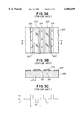
- FIG. 8A is a plan view showing a structure of a photomask according to a first embodiment of the present invention
- FIG. 8B is a sectional view taken on line E--E of FIG. 8A.
- the first embodiment is a photomask which is used for a KrF excimer laser exposure equipment with annular illumination in which a ratio between pattern sizes of a mask pattern and an image plane, that is a reducing magnification, is 1/5, a numerical aperture NA is 0.55 and a light interception ratio is 50%. That the light interception ratio is 50% shows that the maximum coherence factor is 0.8 and a coherence factor in the central portion is 0.4.
- a photomask according to the first embodiment has a light intercepting film 102 made of chromium as a main component on a transparent substrate 101 made of synthetic quartz, as shown in FIGS. 8A and 8B.
- a main pattern region 1 of 0.9 ⁇ m square is divided on the transparent substrate 101. With this, an isolated hole pattern of 0.18 ⁇ m square is to be formed on an image plane.
- Hole pattern regions each of 0.9 ⁇ m square whose sides are made of four sides parallel to the respective sides of the main pattern region 1 are partitioned as auxiliary pattern regions 2a, 2b, 2c or 2d, wherein the auxiliary pattern regions 2a, 2b, 2c and 2d are respectively opposed to the four sides of the main pattern region 1.
- Distances between the respective auxiliary pattern regions 2a, 2b, 2c or 2d and the main pattern region 1 are 0.9 ⁇ m. Openings are formed at positions in alignment with the main pattern region 1 or the auxiliary pattern regions 2a, 2b, 2c or 2d in the light intercepting film 102. As shown in FIG.
- the auxiliary pattern regions 2a, 2b, 2c and 2d of the transparent substrate 101 each are etched to a depth of, for example, 496 nm to form an etching step portion 3. Since a refractive index of the transparent substrate 101 made of synthetic quartz is 1.5 and a etched depth is 496 nm, a phase difference of 360 degrees arises between light transmitted through any of the auxiliary patter regions 2a, 2b, 2c and 2d and light transmitted through the main pattern 1 in the case where excimer laser light of a wavelength of 248 nm is used.
- the effect to reduce light intensity in the etching step portion 3 is applied to prevent transferring of an auxiliary pattern from occurring in the case of a photomask according to the first embodiment of the present invention constructed as mentioned above. That is, since an influence of the side wall of an etching step portion 3 acts to a region in the vicinity thereof, no much influence is given to exposure characteristics of the main pattern region and only transferring of an auxiliary pattern region is prevented from occurring.
- FIG. 9 is a typical view showing a phase of light in a etching step portion.
- Two-dot chain lines show planes of the same phase of light transmitted in FIG. 9.
- FIG. 9 in the vicinity of the side wall of the etching step portion 3, projection and reflection of light occur and thereby there arises a region 3a where a phase is in disorder, that is the phase difference is other than of zero degree or 360 degrees.
- a depth of the etching step portions 3 thereof may properly be set.
- the depth of the etching step portion 3 is set so that a phase difference of 360 degrees may occur in consideration of the relation between a phase difference and an exposure characteristics. Therefore, with use under off-axis illumination, such as annular illumination or the like, the depth of focus is increased. Moreover, if the phase difference is a value of an integral number of times of 360 degrees except for zero degree, a similar effect can be achieved.
- auxiliary pattern regions 2a, 2b, 2c and 2d of about the same size as that of a main pattern region 1 are formed, the depth of focus of the main pattern region 1 can be increased.
- FIG. 10 is a SEM photograph showing a pattern transferred to photosensitive resin with use of a photomask according to the first embodiment. As can be seen from FIG. 10, while an isolated hole pattern with a high accuracy is formed in photosensitive resin, auxiliary pattern regions of the same size as that of the main pattern region 1 is not resolved in the resin. This is an influence of the side wall of an etching step portion 3.
- FIG. 11 is a SEM photograph showing a pattern transferred to photosensitive resin with use of a photomask for a hole pattern of 0.2 ⁇ m square.
- the upper limit of the same size at which a main pattern region and auxiliary pattern regions can be designed is 0.2 ⁇ m.
- a size of each of auxiliary pattern regions is still required to be set 0.2 ⁇ m, since if not, the auxiliary pattern regions are transferred.
- auxiliary pattern regions are set on the order of 0.7 to 1 times of that of a main pattern region, a size of the auxiliary pattern regions can be determined at a level at which they are not transferred.
- the present invention is not limited to a photomask for an isolated hole pattern, but also applicable to photomasks, for example, a lines and spaces pattern and the like.
- FIG. 12A is a plan view showing a structure of a photomask according to a second embodiment of the present invention and FIG. 12B is a sectional view taken on line F--F of FIG. 12A.
- a light intercepting film 112 made of chromium as a main component formed on a transparent substrate 111 made of synthetic quartz.
- a main pattern region 11 having a line like shape is divided on the transparent substrate 111.
- Auxiliary patterns 12a and 12b extending along the same direction as that of the main pattern region 11 are divided on the sides, left and right, thereof as viewed.
- auxiliary pattern regions in the case of a lines and spaces pattern is easier to be resolved than the case of a hole space, a width of each of the auxiliary pattern regions is required to be formed somewhat smaller than that of the main pattern region.
- the reason why is that, while in the case of a hole pattern influences of the side wall of an etching step portion formed in auxiliary regions come from the four points, in the case of a lines and spaces pattern influences of the side wall come from two points only.
- a size of a main pattern region is 1 ⁇ m
- a size of an auxiliary pattern region is, for example, 0.9 ⁇ m.
- auxiliary pattern regions 12a and 12b in the transparent substrate 111 each are etched to a depth of 496 nm to form etching step portions 13.
- a main pattern region may be a repetition pattern, wherein the pattern is not a perfectly isolated pattern.
- FIG. 13 is a plan view showing a structure of photomask according to a third embodiment of the present invention.
- plural main pattern regions 21 are arranged in a grid like shape at constant distance between adjacent patterns and a main pattern region group 24 comprises these plural main pattern regions 21.
- Plural auxiliary pattern regions 22 of the same size as that of a main pattern regions 21 are divided at constant distances in the outer periphery of the main pattern region group 24.
- An auxiliary pattern region group 25 comprises plural auxiliary pattern regions 22.
- a transparent substrate is etched to a depth corresponding to a phase difference of 360 degrees in each of the auxiliary pattern regions 22.
- FIG. 14 is a plan view showing a structure of photomask according to a fourth embodiment of the present invention.
- plural main pattern regions 31 are periodically divided along one direction and a main pattern region group 34 comprises the plural main pattern regions 31.
- Plural auxiliary pattern regions 32 are disposed at constant distances in the outer periphery of the main pattern region group 34.
- An auxiliary pattern region group 35 comprises plural pattern regions 32.
- a transparent substrate is etched to a depth corresponding to a phase difference of 360 degrees in each of the auxiliary pattern regions 32.
- an auxiliary pattern region group 35 is divided in the outer periphery of a main pattern region group 34 and a pattern structure with a multidirectional periodicity is adopted, so that a depth of focus is made increased.
- phase difference is a value of any multiples of 360 degrees, such as 360, 720, 1080 or the like.
- the reason why is that resolution characteristics of a main pattern region are changed according to a phase difference with an auxiliary pattern region.
- FIGS. 15A to 15F are graphs showing relations between the defocus and the light intensity distribution in various phase differences, wherein positions on an image plane are plotted on the axis of abscissa and values of relative light intensity are plotted on the axis of ordinate.
- a solid line indicates the best focus and a broken line indicates a defocus of -0.5 ⁇ m and a dotted line indicates a defocus of +0.5 ⁇ m.
- the relations shown in FIGS. 15A to 15F are obtained in simulation by use of a lithography simulator on the market Porlith/2 made by FINLE Technologies, Inc.
- FIGS. 15A to 15E respectively show relations in the cases of phase differences of zero, 45, 90, 135 and 180 in that order and FIG. 15F shows a comparative example where no auxiliary pattern regions are provided.
- phase differences shown in FIGS. 15B, 15C or 15D respectively are 45, 90 and 135 degrees of phase differences
- light intensity distributions are different according to +/- signs of the defocus.
- a phase difference is a value of an integral number of times of 180 degrees from a view point of a pattern size control.
- FIGS. 15A and 15E when light intensities are compared with each other between phase differences of 0 degree and 180 degrees, the case of a phase difference of 0 degree shown in FIG. 15A has a steeper image.
- a quality of a transferred image of a main pattern region is evaluated by a new contrast NC defined by the following mathematical formula (3), which is:
- FIG. 16 is representation illustrating I max and I edge and shows relations among a photomask, a light intensity distribution of light transmitted through the photomask and a pattern formed on photosensitive resin by transmitted light.
- a photomask 123 comprising a transparent substrate 121 and a light intercepting film 122 formed thereon as shown in FIG. 16
- transmitted light through the photomask 123 shows a relative intensity distribution like a normal distribution.
- the maximum light intensity I max is to show the maximum of the relative light intensity.
- the light intensity I edge at a pattern edge at the best focus is to show a light intensity at the boundary between the light intercepting film and the transparent region of the photomask 123.
- To adjust a light intensity I edge at a pattern edge at the best focus is corresponds to setting an exposure dose so that a pattern size of photosensitive resin 124 formed on a semiconductor substrate 125 at the best focus may be a target value.
- an pattern forming process such as an exposure step, a developing step and the like of the photosensitive resin 124
- the process can, in a simplified manner, be considered to proceed in such a manner that development is vertically advanced from a point where a light intensity shows its maximum till the development reaches the bottom portion and thereafter the development is turned along a horizontal direction, so that photosensitive resin 124 is processed to form an opening of a predetermined size.
- a value of the new contrast NC at which pattern formation is possible in photosensitive resin 124 is dependent on a performance of the photosensitive resin 124 and as a resolving power is higher, a pattern can formed with a lower new contrast NC.
- the limit is in the range of 1.4 to 1.6.
- FIG. 17 is a graph showing a relation between the phase difference and the new contrast NC in various defocus conditions, wherein values of the phase difference between light transmitted through a main pattern and light transmitted through an auxiliary pattern are plotted on the axis of abscissa and values of the new contrast are plotted on the axis of ordinate.
- a solid line indicates the best focus and a broken line indicates a defocus of -0.5 ⁇ m and a dotted line indicates a defocus of +0.5 ⁇ m.
- a new contrast NC at the best focus in the case where a defocus is 0 ⁇ m is conspicuously higher than those in the cases where a defocus is +0.5 or -0.5 ⁇ m.
- a new contrast NC assumes the highest value at a phase difference of 0 or 360 degrees and the lowest at a phase difference of 180 degrees. Therefore, it is desired that a phase difference assumes a value of an integral number of times of 360 degrees.
- FIG. 18 is a graph showing a relation between the defocus and the new contrast NC on various photomasks.
- FIG. 18 is a graph showing a relation between the defocus and the new contrast NC on various photomasks, wherein values of the defocus are plotted on the axis of abscissa and values of the new contrast NC are plotted on the axis of ordinate.
- a solid line indicates the case where a photomask of the present invention, which produces a phase shift of 360 degrees is used and a broken line indicates the case of an conventional photomask in which no auxiliary pattern regions are provided.
- the values of new contrast NC are improved by providing an auxiliary pattern region.
- a depth of focus is increase to +0.3 ⁇ m with use of a photomask of the embodiment, while a depth of focus is +0.2 ⁇ m with use of a conventional mask.
- an actual depth of focus can be increased from ⁇ 0.2 ⁇ m to ⁇ 0.3 ⁇ m.
- FIG. 19A is a plan view showing a structure of a photomask according to a fifth embodiment of the present invention and FIG. 19B is a sectional view taken on line G--G of FIG. 19A.
- the fifth embodiment is a photomask for the same exposure equipment as that of the first embodiment. That is, exposure conditions are the same as those in the first embodiment.
- a pattern formed on photosensitive resin is an isolated pattern of 0.18 ⁇ m square.
- a semitransparent film 142 made of chromium oxynitride is formed on a transparent substrate 141 made of synthetic quartz.
- a film thickness of the semitransparent film 142 is 120 nm and there arises a phase difference of 180 degrees between light transmitted through the semitransparent 142 and light not transmitted therethrough.
- a main pattern region 41 of 0.9 ⁇ m square is divided on the transparent substrate 141. Thereby, a hole pattern of 0.18 ⁇ m square is to be formed on an image plane.
- Hole pattern regions each of 0.9 ⁇ m square constructed of four sides respectively parallel to four sides of the main pattern region 41 are divided in the outer periphery as auxiliary pattern regions 42a, 42b, 42c and 42d so that the hole pattern regions 42a, 42b, 42c and 42d are respectively opposed to the four sides of the main pattern region 41.
- a distance between the main pattern region 41 and any of the auxiliary pattern regions 42a, 42b, 42c and 42d is 0.9 am.
- the transparent substrate 142 is etched at the auxiliary pattern regions 42a, 42b, 42c and 42d each to a depth of, for example, 248 nm and an etching step portion 43 is formed.
- auxiliary pattern regions 42a, 42b, 42c and 42d are not transferred because of an influence of the side wall of the etching step portion 43.
- a phase difference between light transmitted through the main pattern region 41 and light transmitted through the auxiliary pattern regions 42a, 42b, 42c and 42d is a value of an integral number of times as large as 360 degrees except for 0.
- a phase difference for example 720, 1080 degrees or the like, may be produced by adjusting a depth of the etching step portion.
- auxiliary pattern regions each of substantially the same size as that of a main pattern region in the case where a depth of focus is short and a size of each of the auxiliary pattern regions is a size of a fine pattern near the limit of required resolution.
- FIG. 20A is a plan view showing a structure of a photomask according to a sixth embodiment of the present invention and FIG. 20B is a sectional view taken on line H--H of FIG. 20A.
- the sixth embodiment is a photomask for use in a projection equipment with an numerical aperture NA of 0.55 and a coherence factor ⁇ of 0.36.
- a pattern formed in photosensitive resin is a isolated hole pattern of 0.20 ⁇ m square.
- a light intercepting film 152 made of chromium is formed on a transparent 151 made of quartz as shown in FIG. 20A and 20B.
- a main pattern region 51 of 1 ⁇ m square is divided on the transparent substrate 151. Thereby, an isolated hole pattern of 0.2 ⁇ m square is to be formed on an image plane.
- Hole pattern regions each of 1 ⁇ m square constructed of four sides respectively parallel to four sides of the main pattern region 51 are partitioned in the outer periphery as auxiliary pattern regions 52a, 52b, 52c and 52d so that the hole pattern regions 52a, 52b, 52c and 52d are respectively opposed to the four sides of the main pattern region 51.
- a distance between the main pattern region 51 and any of the auxiliary pattern regions 52a, 52b, 52c and 52d is 1 ⁇ m.
- the transparent substrate 151 is etched at the auxiliary pattern regions 52a, 52b, 52c and 52d each to a depth of, for example, 248 nm and an etching step portion 53 is formed.
- the embodiment is an application of a so-called Shibuya-Levenson type phase shift mask.
- FIG. 21 is a SEM photograph showing a pattern transferred to photosensitive resin with use of a photomask according to the sixth embodiment.
- FIG. 21 shows a pattern when a coherence factor ⁇ is set 0.4 in order to obtain an effect of a phase shift mask of a Shibuya-Levenson type.
- the auxiliary patterns 52a, 52b, 52c and 52d are almost not transferred as in the first embodiment and only the main pattern region 51 is transferred to form an isolated hole pattern.
- the embodiment is an application of a phase shift mask of a Shibuya-Levenson type, a resolution and a depth of focus thereof is higher as compared with the first embodiment.
- a depth of focus of 1.2 ⁇ m is obtained for a hole pattern of 0.2 ⁇ m and a hole pattern of 0.16 ⁇ m was able to be resolved.
- a phase difference of an auxiliary pattern region is equal to or an odd number of times of 180 degrees.
- FIGS. 22A to 22F are graphs showing a relation between the defocus and the light intensity distribution in various phase differences, wherein positions on an image plane are plotted on the axis of abscissa and values of the relative light intensity are plotted on the axis of ordinate.
- FIGS. 22A to 22E respectively show the cases of phase differences of 0, 45, 90, 135, 180 degrees in that order and
- FIG. 22F shows an comparative example in which no auxiliary pattern regions are provided. Besides, in FIGS.
- a solid line shows the best focus
- a broken line shows a defocus of -0.5 ⁇ m
- a dotted line shows a defocus of +0.5 ⁇ m.
- the sharpest image has been obtained in the case of a phase difference of 180 degrees.
- FIG. 23 is a graph showing a relation between the phase difference and the new contrast NC in various defocus conditions, wherein values of the phase difference between light transmitted through a main pattern region and light transmitted through an auxiliary pattern region are plotted on the axis of abscissa and values of the new contrast NC are plotted on the axis of ordinate.
- a solid line indicates the best focus
- a broken line indicates a defocus of -0.5 ⁇ m
- a dotted line indicates a defocus of +0.5 ⁇ m.
- a new contrast NC is the highest at a phase difference of 180 degrees as well.
- a depth of focus can be the maximum when a phase difference assumes a value of an odd number of times as large as 180 degrees, such as 180, 540 and the like. That is, the steepest transferred image can be obtained when a phase difference assumes a value of an odd number of times as large as 180 degrees.
- FIG. 24 is a graph showing a relation between the defocus and the new contrast NC on various photomasks, wherein values of the defocus are potted on the axis of abscissa and values of the new contrast NC are plotted on the axis of ordinate.
- a solid line indicates the case of a photomask of the embodiment in which a phase of 180 degrees arises
- a broken line shows the case of a conventional photomask in which no auxiliary patters are not provided.
- a depth of focus is increased by a great margin to ⁇ 0.53 ⁇ m for a photomask of the embodiment, while a depth of focus is ⁇ 0.23 ⁇ m for an ordinary photomask.
- an upper limit of a size of an auxiliary pattern region at which the region is not transferred is changed according to exposure conditions, a pattern shape and a pattern size. For this reason, it is necessary to confirm an upper limit thereof in each condition within about the range of 0.7 to 1 times of that of a main pattern region.
- auxiliary pattern regions each of substantially the same size as that of a main pattern region in the case where a depth of focus is short and a size of each of the auxiliary pattern regions is a size of a fine pattern near the limit of required resolution.
Landscapes
- Physics & Mathematics (AREA)
- General Physics & Mathematics (AREA)
- Preparing Plates And Mask In Photomechanical Process (AREA)
- Exposure And Positioning Against Photoresist Photosensitive Materials (AREA)
Applications Claiming Priority (2)
| Application Number | Priority Date | Filing Date | Title |
|---|---|---|---|
| JP4634097A JP2988417B2 (ja) | 1997-02-28 | 1997-02-28 | フォトマスク |
| JP9-046340 | 1997-02-28 |
Publications (1)
| Publication Number | Publication Date |
|---|---|
| US6004699A true US6004699A (en) | 1999-12-21 |
Family
ID=12744417
Family Applications (1)
| Application Number | Title | Priority Date | Filing Date |
|---|---|---|---|
| US09/031,107 Expired - Fee Related US6004699A (en) | 1997-02-28 | 1998-02-26 | Photomask used for projection exposure with phase shifted auxiliary pattern |
Country Status (3)
| Country | Link |
|---|---|
| US (1) | US6004699A (ko) |
| JP (1) | JP2988417B2 (ko) |
| KR (1) | KR100306415B1 (ko) |
Cited By (22)
| Publication number | Priority date | Publication date | Assignee | Title |
|---|---|---|---|---|
| WO2001037053A1 (en) * | 1999-11-15 | 2001-05-25 | Asm Lithography B.V. | Imaging method using phase boundary masking with modified illumination |
| US6421820B1 (en) * | 1999-12-13 | 2002-07-16 | Infineon Technologies Ag | Semiconductor device fabrication using a photomask with assist features |
| US6466304B1 (en) * | 1998-10-22 | 2002-10-15 | Asm Lithography B.V. | Illumination device for projection system and method for fabricating |
| US6511048B1 (en) * | 1998-07-16 | 2003-01-28 | Hitachi, Ltd. | Electron beam lithography apparatus and pattern forming method |
| US6670646B2 (en) | 2002-02-11 | 2003-12-30 | Infineon Technologies Ag | Mask and method for patterning a semiconductor wafer |
| WO2004006015A2 (de) * | 2002-07-05 | 2004-01-15 | Infineon Technologies Ag | Verfahren zum bestimmen des aufbaus einer maske zum mikrostrukturieren von halbleitersubstraten mittels fotolithographie |
| US20040033424A1 (en) * | 2002-08-15 | 2004-02-19 | Talin Albert Alec | Lithographic template and method of formation and use |
| US6709791B1 (en) * | 1999-08-18 | 2004-03-23 | Dai Nippon Printing Co., Ltd. | Halftone phase shift photomask and blanks for halftone phase shift photomask for it and pattern forming method using this |
| US6800401B2 (en) * | 2000-04-27 | 2004-10-05 | Petersen Advanced Lithography, Inc. | Method for phase shift mask design, fabrication, and use |
| US20050166238A1 (en) * | 2004-01-08 | 2005-07-28 | Vitito Christopher J. | Automobile entertainment system |
| US20050277032A1 (en) * | 2004-06-14 | 2005-12-15 | Photronics, Inc. 15 Secor Road P.O. Box 5226 Brookfield, Connecticut 06804 | Photomask reticle having multiple versions of the same mask pattern with different biases |
| US20050277033A1 (en) * | 2004-06-14 | 2005-12-15 | Phototronics, Inc. 15 Secor Road P.O. Box 5226 Brookfield, Connecticut 06804 | Method of forming a semiconductor layer using a photomask reticle having multiple versions of the same mask pattern with different biases |
| US20060051683A1 (en) * | 2004-09-09 | 2006-03-09 | Fujitsu Limited | Method of manufacturing mask for exposure, mask for exposure, and package body of mask for exposure |
| US20060292454A1 (en) * | 2003-08-15 | 2006-12-28 | Hoya Corporation | Method of producing phase shift masks |
| US20070003841A1 (en) * | 2005-06-29 | 2007-01-04 | Hynix Semiconductor Inc. | Double exposure method and photomask for same |
| US20070190434A1 (en) * | 2006-02-16 | 2007-08-16 | Hoya Corporation | Pattern forming method and phase shift mask manufacturing method |
| US20080055577A1 (en) * | 2006-08-30 | 2008-03-06 | Asml Netherlands B.V. | Lithographic apparatus and method |
| US20080138728A1 (en) * | 2006-11-30 | 2008-06-12 | Akihiro Sugino | Latent electrostatic image bearing member, and image forming apparatus, image forming method and process cartridge using the same |
| US20100129736A1 (en) * | 2008-06-17 | 2010-05-27 | Kasprowicz Bryan S | Photomask Having A Reduced Field Size And Method Of Using The Same |
| US20110086511A1 (en) * | 2009-06-17 | 2011-04-14 | Kasprowicz Bryan S | Photomask having a reduced field size and method of using the same |
| US8846273B2 (en) * | 2012-06-04 | 2014-09-30 | Micron Technology, Inc. | Photomasks, methods of forming a photomask, and methods of photolithographically patterning a substrate |
| US20210335599A1 (en) * | 2020-04-28 | 2021-10-28 | Taiwan Semiconductor Manufacturing Co., Ltd. | Euv photomask and related methods |
Families Citing this family (11)
| Publication number | Priority date | Publication date | Assignee | Title |
|---|---|---|---|---|
| JP3275863B2 (ja) | 1999-01-08 | 2002-04-22 | 日本電気株式会社 | フォトマスク |
| KR100353406B1 (ko) * | 2000-01-25 | 2002-09-18 | 주식회사 하이닉스반도체 | 위상 반전 마스크 및 그 제조 방법 |
| JP3768794B2 (ja) * | 2000-10-13 | 2006-04-19 | 株式会社ルネサステクノロジ | 半導体集積回路装置の製造方法 |
| JP2002357889A (ja) * | 2001-03-28 | 2002-12-13 | Sony Corp | 位相シフトマスクの作製装置及び作製方法並びに位相シフトマスクを使用するパターン形成方法 |
| JP2004348118A (ja) | 2003-04-30 | 2004-12-09 | Toshiba Corp | フォトマスク及びそれを用いた露光方法、データ発生方法 |
| JP2007286362A (ja) * | 2006-04-17 | 2007-11-01 | Toshiba Corp | リソグラフィシミュレーション方法、プログラム及び半導体装置の製造方法 |
| JP5085366B2 (ja) * | 2008-02-14 | 2012-11-28 | Hoya株式会社 | フォトマスクの欠陥修正方法及びフォトマスクの製造方法 |
| JP4702903B2 (ja) * | 2008-10-27 | 2011-06-15 | Hoya株式会社 | 位相シフトマスクの製造方法 |
| JP2012234057A (ja) * | 2011-05-02 | 2012-11-29 | Elpida Memory Inc | フォトマスクおよび半導体装置 |
| JP5229838B2 (ja) * | 2011-11-09 | 2013-07-03 | Hoya株式会社 | マスクブランク及びフォトマスク |
| US10811492B2 (en) | 2018-10-31 | 2020-10-20 | Texas Instruments Incorporated | Method and device for patterning thick layers |
Citations (7)
| Publication number | Priority date | Publication date | Assignee | Title |
|---|---|---|---|---|
| JPS5762052A (en) * | 1980-09-30 | 1982-04-14 | Nippon Kogaku Kk <Nikon> | Original plate to be projected for use in transmission |
| JPH0315845A (ja) * | 1989-06-14 | 1991-01-24 | Hitachi Ltd | マスク及びマスク作製方法 |
| JPH04136854A (ja) * | 1990-09-28 | 1992-05-11 | Hitachi Ltd | 半導体装置の製造方法 |
| JPH04268714A (ja) * | 1991-02-25 | 1992-09-24 | Nikon Corp | 露光方法、半導体素子の形成方法、及びフォトマスク |
| JPH05333524A (ja) * | 1992-06-04 | 1993-12-17 | Nec Corp | 位相シフトマスクおよびその製造方法 |
| JPH0777796A (ja) * | 1993-09-10 | 1995-03-20 | Fujitsu Ltd | 露光用マスク及び露光方法 |
| JPH08194303A (ja) * | 1995-01-19 | 1996-07-30 | Hitachi Ltd | 位相シフトマスクおよびその製造方法 |
-
1997
- 1997-02-28 JP JP4634097A patent/JP2988417B2/ja not_active Expired - Fee Related
-
1998
- 1998-02-26 US US09/031,107 patent/US6004699A/en not_active Expired - Fee Related
- 1998-02-27 KR KR1019980006453A patent/KR100306415B1/ko not_active IP Right Cessation
Patent Citations (7)
| Publication number | Priority date | Publication date | Assignee | Title |
|---|---|---|---|---|
| JPS5762052A (en) * | 1980-09-30 | 1982-04-14 | Nippon Kogaku Kk <Nikon> | Original plate to be projected for use in transmission |
| JPH0315845A (ja) * | 1989-06-14 | 1991-01-24 | Hitachi Ltd | マスク及びマスク作製方法 |
| JPH04136854A (ja) * | 1990-09-28 | 1992-05-11 | Hitachi Ltd | 半導体装置の製造方法 |
| JPH04268714A (ja) * | 1991-02-25 | 1992-09-24 | Nikon Corp | 露光方法、半導体素子の形成方法、及びフォトマスク |
| JPH05333524A (ja) * | 1992-06-04 | 1993-12-17 | Nec Corp | 位相シフトマスクおよびその製造方法 |
| JPH0777796A (ja) * | 1993-09-10 | 1995-03-20 | Fujitsu Ltd | 露光用マスク及び露光方法 |
| JPH08194303A (ja) * | 1995-01-19 | 1996-07-30 | Hitachi Ltd | 位相シフトマスクおよびその製造方法 |
Cited By (39)
| Publication number | Priority date | Publication date | Assignee | Title |
|---|---|---|---|---|
| US6511048B1 (en) * | 1998-07-16 | 2003-01-28 | Hitachi, Ltd. | Electron beam lithography apparatus and pattern forming method |
| US6466304B1 (en) * | 1998-10-22 | 2002-10-15 | Asm Lithography B.V. | Illumination device for projection system and method for fabricating |
| USRE40239E1 (en) * | 1998-10-22 | 2008-04-15 | Asml Netherlands B.V. | Illumination device for projection system and method for fabricating |
| US6709791B1 (en) * | 1999-08-18 | 2004-03-23 | Dai Nippon Printing Co., Ltd. | Halftone phase shift photomask and blanks for halftone phase shift photomask for it and pattern forming method using this |
| WO2001037053A1 (en) * | 1999-11-15 | 2001-05-25 | Asm Lithography B.V. | Imaging method using phase boundary masking with modified illumination |
| US6421820B1 (en) * | 1999-12-13 | 2002-07-16 | Infineon Technologies Ag | Semiconductor device fabrication using a photomask with assist features |
| US6800401B2 (en) * | 2000-04-27 | 2004-10-05 | Petersen Advanced Lithography, Inc. | Method for phase shift mask design, fabrication, and use |
| US6670646B2 (en) | 2002-02-11 | 2003-12-30 | Infineon Technologies Ag | Mask and method for patterning a semiconductor wafer |
| US20050148195A1 (en) * | 2002-07-05 | 2005-07-07 | Infineon Technologies Ag | Method for determining the construction of a mask for the micropatterning of semiconductor substrates by means of photolithography |
| WO2004006015A2 (de) * | 2002-07-05 | 2004-01-15 | Infineon Technologies Ag | Verfahren zum bestimmen des aufbaus einer maske zum mikrostrukturieren von halbleitersubstraten mittels fotolithographie |
| WO2004006015A3 (de) * | 2002-07-05 | 2004-05-27 | Infineon Technologies Ag | Verfahren zum bestimmen des aufbaus einer maske zum mikrostrukturieren von halbleitersubstraten mittels fotolithographie |
| US6993455B2 (en) * | 2002-07-05 | 2006-01-31 | Infineon Technologies Ag | Method for determining the construction of a mask for the micropatterning of semiconductor substrates by means of photolithography |
| US7083880B2 (en) | 2002-08-15 | 2006-08-01 | Freescale Semiconductor, Inc. | Lithographic template and method of formation and use |
| WO2004017388A3 (en) * | 2002-08-15 | 2004-08-12 | Motorola Inc | Lithographic template and method of formation |
| WO2004017388A2 (en) * | 2002-08-15 | 2004-02-26 | Freescale Semiconductor, Inc. | Lithographic template and method of formation |
| US20060222968A1 (en) * | 2002-08-15 | 2006-10-05 | Freescale Semiconductor, Inc. | Lithographic template and method of formation and use |
| US7432024B2 (en) | 2002-08-15 | 2008-10-07 | Freescale Semiconductor, Inc. | Lithographic template and method of formation and use |
| US20040033424A1 (en) * | 2002-08-15 | 2004-02-19 | Talin Albert Alec | Lithographic template and method of formation and use |
| US7678509B2 (en) * | 2003-08-15 | 2010-03-16 | Hoya Corporation | Method of producing phase shift masks |
| US20060292454A1 (en) * | 2003-08-15 | 2006-12-28 | Hoya Corporation | Method of producing phase shift masks |
| US20050166238A1 (en) * | 2004-01-08 | 2005-07-28 | Vitito Christopher J. | Automobile entertainment system |
| US20050277032A1 (en) * | 2004-06-14 | 2005-12-15 | Photronics, Inc. 15 Secor Road P.O. Box 5226 Brookfield, Connecticut 06804 | Photomask reticle having multiple versions of the same mask pattern with different biases |
| US20050277033A1 (en) * | 2004-06-14 | 2005-12-15 | Phototronics, Inc. 15 Secor Road P.O. Box 5226 Brookfield, Connecticut 06804 | Method of forming a semiconductor layer using a photomask reticle having multiple versions of the same mask pattern with different biases |
| US7435533B2 (en) | 2004-06-14 | 2008-10-14 | Photronics, Inc. | Method of forming a semiconductor layer using a photomask reticle having multiple versions of the same mask pattern with different biases |
| US7396617B2 (en) | 2004-06-14 | 2008-07-08 | Photronics, Inc. | Photomask reticle having multiple versions of the same mask pattern with different biases |
| US20060051683A1 (en) * | 2004-09-09 | 2006-03-09 | Fujitsu Limited | Method of manufacturing mask for exposure, mask for exposure, and package body of mask for exposure |
| US20070003841A1 (en) * | 2005-06-29 | 2007-01-04 | Hynix Semiconductor Inc. | Double exposure method and photomask for same |
| US7771892B2 (en) * | 2005-06-29 | 2010-08-10 | Hynix Semiconductor Inc. | Double exposure method and photomask for same |
| US20070190434A1 (en) * | 2006-02-16 | 2007-08-16 | Hoya Corporation | Pattern forming method and phase shift mask manufacturing method |
| US7674563B2 (en) * | 2006-02-16 | 2010-03-09 | Hoya Corporation | Pattern forming method and phase shift mask manufacturing method |
| US20080055577A1 (en) * | 2006-08-30 | 2008-03-06 | Asml Netherlands B.V. | Lithographic apparatus and method |
| US20080138728A1 (en) * | 2006-11-30 | 2008-06-12 | Akihiro Sugino | Latent electrostatic image bearing member, and image forming apparatus, image forming method and process cartridge using the same |
| US20100129736A1 (en) * | 2008-06-17 | 2010-05-27 | Kasprowicz Bryan S | Photomask Having A Reduced Field Size And Method Of Using The Same |
| US9005848B2 (en) | 2008-06-17 | 2015-04-14 | Photronics, Inc. | Photomask having a reduced field size and method of using the same |
| US20110086511A1 (en) * | 2009-06-17 | 2011-04-14 | Kasprowicz Bryan S | Photomask having a reduced field size and method of using the same |
| US9005849B2 (en) | 2009-06-17 | 2015-04-14 | Photronics, Inc. | Photomask having a reduced field size and method of using the same |
| US8846273B2 (en) * | 2012-06-04 | 2014-09-30 | Micron Technology, Inc. | Photomasks, methods of forming a photomask, and methods of photolithographically patterning a substrate |
| US9075317B2 (en) | 2012-06-04 | 2015-07-07 | Micron Technology, Inc. | Photomasks, methods of forming a photomask, and methods of photolithographically patterning a substrate |
| US20210335599A1 (en) * | 2020-04-28 | 2021-10-28 | Taiwan Semiconductor Manufacturing Co., Ltd. | Euv photomask and related methods |
Also Published As
| Publication number | Publication date |
|---|---|
| KR19980071829A (ko) | 1998-10-26 |
| JPH10239827A (ja) | 1998-09-11 |
| JP2988417B2 (ja) | 1999-12-13 |
| KR100306415B1 (ko) | 2001-10-19 |
Similar Documents
| Publication | Publication Date | Title |
|---|---|---|
| US6004699A (en) | Photomask used for projection exposure with phase shifted auxiliary pattern | |
| US7023522B2 (en) | Multiple exposure method | |
| KR100955293B1 (ko) | 디바이스 제조 방법과 초기 패턴의 패턴 피쳐 분배 방법 및 이러한 방법에 따라서 제조된 디바이스, 리소그래피 서브 마스크 그룹 및 이를 이용하여 제조된 디바이스 | |
| US5827623A (en) | Optical proximity correction halftone type phase shift photomask | |
| US5723235A (en) | Method of producing photomask and exposing | |
| US6605411B2 (en) | Method for formation of semiconductor device pattern, method for designing photo mask pattern, photo mask and process for photo mask | |
| US20020031725A1 (en) | Exposure method, exposure apparatus, and device manufacturing method | |
| US6780574B2 (en) | Multiple exposure method | |
| US5642183A (en) | Spatial filter used in a reduction-type projection printing apparatus | |
| US6811939B2 (en) | Focus monitoring method, focus monitoring system, and device fabricating method | |
| US20090042108A1 (en) | Pattern forming method and mask | |
| US7518707B2 (en) | Exposure apparatus | |
| US5888677A (en) | Exposure mask, method of fabricating same, and method of manufacturing semiconductor device | |
| KR19980071487A (ko) | 위상 시프트 마스크, 노광 방법 및 구면 수차량 측정 방법 | |
| JPH11143047A (ja) | フォトマスク及びその製造方法 | |
| US6451488B1 (en) | Single-level masking with partial use of attenuated phase-shift technology | |
| JP3323815B2 (ja) | 露光方法及び露光装置 | |
| JP3133618B2 (ja) | 縮小投影露光装置において用いられる空間フィルタ | |
| JP5068357B2 (ja) | 半導体装置の製造方法、フォトマスクのパターン設計方法およびフォトマスクの製造方法 | |
| JP3070520B2 (ja) | フォトマスク及び露光方法 | |
| JP2876616B2 (ja) | 投影露光装置 | |
| JPH10115932A (ja) | 位相シフトマスクを用いた露光方法 | |
| JP2959496B2 (ja) | Opcマスク | |
| KR20030043443A (ko) | 반도체 소자의 노광 방법 | |
| KR100826765B1 (ko) | 고립 패턴의 해상력 향상 레티클 제조 방법 및 레티클 구조 |
Legal Events
| Date | Code | Title | Description |
|---|---|---|---|
| AS | Assignment |
Owner name: NEC CORPORATION, JAPAN Free format text: ASSIGNMENT OF ASSIGNORS INTEREST;ASSIGNORS:YASUZATO, TADAO;ISHIDA, SHINJI;REEL/FRAME:009009/0702 Effective date: 19980219 |
|
| FEPP | Fee payment procedure |
Free format text: PAYOR NUMBER ASSIGNED (ORIGINAL EVENT CODE: ASPN); ENTITY STATUS OF PATENT OWNER: LARGE ENTITY |
|
| CC | Certificate of correction | ||
| AS | Assignment |
Owner name: NEC ELECTRONICS CORPORATION, JAPAN Free format text: ASSIGNMENT OF ASSIGNORS INTEREST;ASSIGNOR:NEC CORPORATION;REEL/FRAME:013751/0721 Effective date: 20021101 |
|
| FPAY | Fee payment |
Year of fee payment: 4 |
|
| REMI | Maintenance fee reminder mailed | ||
| LAPS | Lapse for failure to pay maintenance fees | ||
| STCH | Information on status: patent discontinuation |
Free format text: PATENT EXPIRED DUE TO NONPAYMENT OF MAINTENANCE FEES UNDER 37 CFR 1.362 |
|
| FP | Lapsed due to failure to pay maintenance fee |
Effective date: 20071221 |