US6003053A - Pulse signal generation circuit and pulse signal generation method - Google Patents
Pulse signal generation circuit and pulse signal generation method Download PDFInfo
- Publication number
- US6003053A US6003053A US08/971,846 US97184697A US6003053A US 6003053 A US6003053 A US 6003053A US 97184697 A US97184697 A US 97184697A US 6003053 A US6003053 A US 6003053A
- Authority
- US
- United States
- Prior art keywords
- value
- frequency
- addition
- pulse signal
- register
- Prior art date
- Legal status (The legal status is an assumption and is not a legal conclusion. Google has not performed a legal analysis and makes no representation as to the accuracy of the status listed.)
- Expired - Lifetime
Links
Images


Classifications
-
- H—ELECTRICITY
- H03—ELECTRONIC CIRCUITRY
- H03K—PULSE TECHNIQUE
- H03K3/00—Circuits for generating electric pulses; Monostable, bistable or multistable circuits
-
- G—PHYSICS
- G06—COMPUTING; CALCULATING OR COUNTING
- G06F—ELECTRIC DIGITAL DATA PROCESSING
- G06F7/00—Methods or arrangements for processing data by operating upon the order or content of the data handled
- G06F7/60—Methods or arrangements for performing computations using a digital non-denominational number representation, i.e. number representation without radix; Computing devices using combinations of denominational and non-denominational quantity representations, e.g. using difunction pulse trains, STEELE computers, phase computers
- G06F7/68—Methods or arrangements for performing computations using a digital non-denominational number representation, i.e. number representation without radix; Computing devices using combinations of denominational and non-denominational quantity representations, e.g. using difunction pulse trains, STEELE computers, phase computers using pulse rate multipliers or dividers pulse rate multipliers or dividers per se
Definitions
- the present invention relates to a pulse signal generation circuit which outputs a pulse signal generated by dividing a clock pulse signal and to a pulse signal generation method of outputting such a pulse signal.
- the above pulse generation circuit is, as shown in FIG. 16, comprises a counter C for setting a frequency value, a memory M for storing data among which the data corresponding to the frequency value is read by using the frequency value as address signals, a first flip-flop F 1 for latching and outputting data read from the memory, a full adder A for inputting the output of the first flip-flop F 1 , and a second flip-flop F 2 for latching an added value of the full adder A by a predetermined clock signal.
- the above pulse generation circuit adds the output of the first flip-flop F 1 and the output of the second flip-flop F 2 , enters to the counter C a carry signal which is generated by the second flip-flop F 2 when the added value latched by the second flip-flop F 2 exceeds a predetermined value, and outputs the carry signal as a pulse signal of a frequency whose value is set in the counter C until the counter C prohibits the passing of the carry signal.
- this circuit has problems that it is necessary to read data corresponding to the frequency value from the memory M by using the frequency values as address signals so that the first flip-flop F 1 may latch the data. Consequently, the number of processes is increased and the internal structure is complicated, which makes the production of the circuit time-consuming and also brings a disadvantage in terms of operational speed.
- the object of the present invention is to provide a pulse signal generation circuit which can output a pulse signal of a frequency which is other than a power of 2, preventing the internal structure from being complicated and avoiding a decrease in the operational speed.
- a pulse signal generation circuit comprising: a frequency setting register which is at least (n+1) bits long for setting a value of 2 n or smaller as a frequency value of a pulse signal to be generated; and cumulative addition means having an adder and a flip-flop which is at least (n+1) bits long.
- the cumulative addition means repeats at a rate of 2 +1 times per second, operations of making the adder add a value set in the frequency setting register to a value held in the flip-flop and then making the flip-flop hold the addition result, and outputs a signal having a value of (n+1)th bit in the flip-flop as the pulse signal.
- the cumulative addition means makes the adder sequentially accumulates the binary-coded frequency value and holds the accumulated value. Then, while the 2 n+1 clock pulses are inputted, the same number of carries (changes from "0" to "1") as the frequency value occur on the (n+1)th bit. Therefore, the carry signal for the carry, that is, the (n+1)th bit signal becomes a pulse signal of the frequency whose value is set in the frequency setting register. Thus, a pulse signal of a frequency whose value is other than a power of 2 can be outputted.
- a pulse signal generation circuit comprising: a frequency variation register for setting a frequency variation value; an adder-subtracter; addition-subtraction control means for controlling the frequency variation register and the adder-subtracter so as to repeat, at a predetermined calculation interval, operations of adding or subtracting a value set in the frequency setting register and a value set in the frequency variation register with the adder-subtracter and then re-setting a result of the addition or subtraction in the frequency setting register as the frequency value.
- a pulse signal generation method comprising the steps of: setting a value of 2 n or smaller as a frequency value of a pulse signal to be generated in a frequency setting register; cumulatively adding a value set in the frequency setting register at a rate of 2 n+1 times per second; and outputting, as the pulse signal, a signal having a value of (n+1)th bit in the cumulative addition value obtained by the cumulative addition.
- a pulse signal generation method comprising the steps of: setting a frequency variation value in the frequency variation register; cumulatively adding or subtracting a value set in the frequency variation register at a predetermined calculation interval; and re-setting at the calculation interval, a cumulative value of the addition or subtraction obtained by the addition or subtraction at the calculation interval in the frequency setting register as the frequency value.
- FIG. 1 is a block diagram showing the constitution of a pulse generation circuit according to a first embodiment of the present invention
- FIG. 2 is a diagram for illustrating a frequency setting register of the first embodiment
- FIG. 3 shows signal waveforms of a clock pulse signal and an output pulse signal generated in the first embodiment
- FIG. 4 is a block diagram showing the constitution of a pulse generation circuit according to a second embodiment of the present invention.
- FIG. 5 shows changes in the frequency of a pulse signal generated in the second embodiment
- FIG. 6 is a block diagram showing the constitution of an addition-subtraction control circuit in a third embodiment of the present invention.
- FIG. 7 is a block diagram showing the constitution of a pulse generation circuit according to a fourth embodiment of the present invention.
- FIG. 8 is a block diagram showing the constitution of an addition-subtraction control circuit in the fourth embodiment of the present invention.
- FIG. 9 is a block diagram showing the constitution of a pulse generation circuit according to a fifth embodiment of the present invention.
- FIG. 10 shows changes in the frequency of a pulse signal generated in the sixth embodiment
- FIG. 11 is a block diagram showing the constitution of a pulse generation circuit according to a seventh embodiment of the present invention.
- FIG. 12 shows changes in the frequency of a pulse signal generated in the seventh embodiment
- FIG. 13 is a block diagram showing a circuit in a CPU for generating an addition-subtraction indicative signal in the sixth embodiment
- FIG. 14 is a flowchart illustrating the operation of the CPU for generating the addition-subtraction indicative signal in the sixth embodiment
- FIG. 15 shows changes in the frequency of a pulse signal generated in a eighth embodiment.
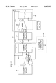
- FIG. 16 is a block diagram illustrating a pulse signal generation circuit according to a prior art.
- This pulse signal generation circuit comprises a frequency setting register 1, an oscillator 20, and a cumulative addition circuit 22 having an adder 2 and a flip-flop 3.
- the frequency setting register 1 is used for setting a frequency value of 2 n or smaller, and has (n+1) bits consisting of the 0-th bit 1 0 of the first bit through the n-th bit 1 n of the (n+1)th bit as shown in FIG. 2. To be more specific, via a (n+1) bit bus 4a the frequency value is set into the frequency setting register 1.
- the adder 2 is connected to the frequency setting register 1 by a (n+1) bit bus 4b so as to make it possible to add the frequency value set in the frequency setting register 1.
- the oscillator 20 generates a clock pulse signal of 2 n+1 Hz and supplies it to the signal input terminal 3a of the flip-flop 3.
- the flip-flop 3 is (n+1) bits long. Every time a clock pulse is inputted from the clock pulse signal input terminal 3a, the flip-flop 3 makes the adder 2 connected via a (n+1) bit bus 5a add the frequency value and holds the added value until the next clock pulse is inputted. The flip-flop 3 further feedbacks the added value to the adder 2 via a (n+1) bit bus 5b and makes the adder 2 sequentially accumulate (cumulative addition) the frequency value. Through these processes, in the accumulated value held in the flip-flop 3, the same number of carries (changes from "0" to "1") as the frequency value occur on the (n+1)th bit while 2 n+1 clock pulses are being inputted.
- the binary-coded number of the decimal number "2" namely "10” is sequentially added starting at the initial value "00" by the adder 2
- the accumulated value is held in the frequency setting register 1.
- "1" is carried to the second bit.
- the binary-coded number of the decimal number "3" namely, "11” is sequentially added starting at the initial value "00" by the adder 2
- the accumulated value is held in the frequency setting register 1.
- "1" is carried to the third bit.
- a change from "0" to "1" (a carry) occurs three times on the third bit, and when the carry signal for the carry is outputted, a pulse signal whose frequency is 3 Hz is outputted.
- the flip-flop 3 makes the adder 2 sequentially accumulate the frequency value converted to binary numbers and holds the accumulated value. Then, while the 2 n+1 clock pulses are inputted, the same number of carries (changes from "0" to "1") as the frequency value occur on the (n+1)th bit. Therefore, the carry signal for the carry, that is, the (n+1)th bit signal becomes a pulse signal of the frequency whose value is set in the frequency setting register 1. Thus, a pulse signal of a frequency whose value is other than a power of 2 can be outputted.
- the second embodiment of the present invention will be described as follows, based on FIGS. 4 and 5.
- the elements substantially having the same functions as those of the first embodiment are referred to with the same reference numbers, and the following description will be focused on the features different from the first embodiment.
- a frequency value to be set in the frequency setting register is fixed in the first embodiment, it is variable in the present embodiment.
- this pulse signal generation circuit comprises a frequency variation register 6, an addition-subtraction circuit 7, and an addition-subtraction controller 8, in addition to the elements of the first embodiment.
- the frequency variation register 6 is used for setting a frequency variation value and is n bits long.
- the addition-subtraction circuit 7 is connected to the frequency variation register 6 via a (n+1) bit bus 4c so as to add or subtract the frequency variation value set in the frequency variation register 6.
- This addition-subtraction circuit 7 is connected to the frequency setting register 1 via the (n+1) bit bus 4a so as to make the frequency setting register 1 input the added or subtracted value.
- the addition-subtraction circuit 7 is also connected to the frequency setting register 1 via a (n+1) bit feedback bus 4d which feedbacks the added or subtracted value from the frequency setting register 1, so that the frequency variation value is sequentially accumulated (accumulatively added or subtracted).
- the addition-subtraction controller 8 consists of a CPU and implements an addition-subtraction control means 9.
- This addition-subtraction controller 8 inputs an addition-subtraction indicative signal for designating the calculation interval T 1 of addition and subtraction performed by the addition-subtraction circuit 7, into the frequency setting register 1, and also inputs a mode control signal for controlling the operation in the addition-subtraction circuit 7 (whether to perform addition, or subtraction, or to stop calculation operation), into the addition-subtraction circuit 7.
- the addition-subtraction control means 9 implemented by the addition-subtraction controller 8 so controls that the frequency variation value is sequentially accumulated at the calculation interval T 1 by the addition-subtraction circuit 7, and the accumulated value is inputted as a frequency value to the frequency setting register 1.
- the calculation interval T 1 corresponds to a pulse width or a pulse interval.
- the addition-subtraction controller 8 can input the above-mentioned addition-subtraction indicative signal into the frequency setting register 1 and also can suspend the inputting. In short, the addition-subtraction controller 8 can either supply the signal or suspend the supplying. Consequently, the accumulation as a result of addition and subtraction in the addition-subtraction circuit 7 becomes possible only when the addition-subtraction controller 8 inputs the addition-subtraction indicative signal into the frequency setting register 1, and the interval of the addition-subtraction indicative signal from the addition-subtraction controller 8 becomes the calculation interval T 1 of the addition and subtraction in the addition-subtraction circuit 7.
- the calculation interval T 1 has a fixed interval because the addition-subtraction indicative signal is inputted into the frequency setting register 1 at a fixed interval.
- the pulse generation circuit When a mode control signal from the addition-subtraction controller 8 is inputted into the addition-subtraction circuit 7 and the addition-subtraction indicative signal from the addition-subtraction controller 8 is inputted into the frequency setting register 1, the addition-subtraction circuit 7 adds or subtracts a frequency variation value so as to make the accumulated value that is frequency value. As a result, the frequency value changes by the frequency variation value. In short, the frequency variation value corresponds to a change ⁇ f of the frequency value and the frequency of a pulse signal to be outputted changes as shown in FIG. 5.
- the pulse signal generation circuit in addition to the effects of the first embodiment, when a frequency value become an accumulated value obtained by the sequential accumulation of frequency variation values with the addition-subtraction circuit 7, it changes by a frequency variation value at every calculation interval T 1 under the control of the addition-subtraction control means 9. Consequently, it becomes possible to change the frequency of a pulse signal outputted with a pulse width of the calculation interval T 1 .
- this pulse signal is inputted into a stepping motor, the rotation speed of the stepping motor can be changed.
- the addition-subtraction circuit 7 When the supply of the addition-subtraction indicative signal from the addition-subtraction control means is suspended, the addition-subtraction circuit 7 does not add or subtract the frequency variation value and the accumulated value does not change. As a result, the frequency value in the frequency setting register 1 becomes unchanged, and the frequency of the pulse signal to be outputted is fixed, so that the frequency value which is changed so far can be fixed halfway. Consequently, when this pulse signal is inputted into a stepping motor, the rotation speed of the stepping motor can be changed or maintained.
- the addition-subtraction controller 8 consists of a CPU in the second embodiment
- the addition-subtraction controller 8 in the present embodiment comprises a timing signal register 8a, a control signal register 8b, and a timing cumulative addition circuit 24 having a timing signal addition circuit 8c and a timing designation flip-flop 8d.
- the timing signal register 8a holds a timing signal which can be subjected to an addition by the timing signal addition circuit 8c.
- the control signal register 8b holds an addition control signal which controls the timing signal addition circuit 8c, as well as the above-mentioned mode control signal.
- the timing signal addition circuit 8c operates under the control of the addition control signal of the control signal register 8b, and every time a clock pulse for timing signals is inputted, the timing designation flip-flop 8d holds an accumulated value obtained by the addition in the timing signal addition circuit 8c (cumulatively added value), and outputs a carry signal as the above-mentioned calculation indicative signal intermittently. In short, the interval of the carry signals becomes the calculation interval T 1 .
- This circuit operates in the same manner as the circuit of the second embodiment, under the control of the mode control signal and the addition control signal held in the control signal register 8b of the addition-subtraction controller 8.
- the control signal consisting of the mode control signal and the addition control signal so controls that the accumulated value obtained by the addition-subtraction circuit 7 is inputted as a frequency value to the frequency setting register 1.
- the timing designation flip-flop 8d makes the timing signal addition circuit 8c sequentially accumulate the timing signal and holds the accumulated value.
- the pulse signal generation circuit is controlled by the control signal from the control signal register 8b so that the accumulation value, which is obtained by the accumulation with the addition-subtraction circuit 7 at the calculation interval T 1 that is the interval of the carry signal outputted intermittently from the timing designation flip-flop 8d, is set in the frequency setting register 1.
- the addition and subtraction of the frequency variation value in the addition-subtraction circuit 7 is controlled by supplying the addition-subtraction indicative signal or suspending the supply.
- the addition subtraction control means 9 comprises an input value selection multiplexer 10 which can select between "0" and the frequency variation value, as a value to be inputted into the addition-subtraction circuit 7.
- the input value selection multiplexer 10 controls the addition and subtraction of the frequency variation value in the addition-subtraction circuit 7.
- the input value selection multiplexer 10 is disposed between the frequency variation register 6 and the addition-subtraction circuit 7, and controlled by an input value selection multiplexer control signal which is held in the control signal register 8b of the addition-subtraction controller 8 so as to compose the control signal together with the mode control signal.
- the input value selection multiplexer 10 selects between "0" and the frequency variation value as a value to be inputted into the addition-subtraction circuit 7.
- the addition and subtraction of frequency variation value in the addition-subtraction circuit 7 is controlled by supplying the addition-subtraction indicative signal or suspending the supply of it.
- the addition-subtraction control means 9 comprises a feedback control multiplexer 11 which can select between a feedbacked accumulated value and a re-accumulated value obtained by adding the frequency variation value to the feedbacked accumulated value again in the addition-subtraction circuit 7. The operation of the feedback control multiplexer 11 controls the addition and subtraction of the frequency variation value in the addition-subtraction circuit 7.
- the feedback control multiplexer 11 is disposed between the frequency setting register 1 and the addition-subtraction circuit 7, and connected to the frequency setting register 1 via a (n+1) bit bus 4e so that the accumulated value of the frequency variation value obtained by the addition-subtraction circuit 7 can be inputted directly from the frequency setting register 1.
- the feedback control multiplexer 11 is controlled by a frequency setting multiplexer control signal which is inputted into the control signal register 8b of the addition-subtraction controller 8 so as to compose the control signal together with the mode control signal.
- the multiplexer 11 selects between the accumulated value which is directly inputted from the frequency setting register 1 and the re-accumulated value which is subjected to addition or subtraction again in the addition-subtraction circuit 7, and inputs the selected value into the frequency setting register 1.
- the sixth embodiment of the present invention will be described as follows, based on FIG. 10.
- the elements substantially having the same functions as those of the third embodiment are referred to with the same reference numbers, and the following description will be focused on the features different from the third embodiment.
- the interval of the addition-subtraction indicative signal from the addition-subtraction controller 8, that is, the calculation interval T 1 of the addition and subtraction in the addition-subtraction circuit 7 is fixed.
- the calculation interval T 1 of the addition and subtraction in the addition-subtraction circuit 7 is variable.
- the timing signal in the timing signal register 8a is added so that a carry signal is outputted intermittently at various intervals from the timing designation flip-flop 8d by making an addition control signal in the control signal register 8b control the timing signal addition circuit 8c (see FIG. 6). Since the interval of the carry signal from the timing designation flip-flop 8d is the calculation interval T 1 of addition and subtraction in the addition-subtraction circuit 7, the calculation interval T 1 becomes variable, so as to have the values: T 11 , T 12 , T 13 , T 14 , and the like.
- timing designation flip-flop 8d In order to make the timing designation flip-flop 8d output the carry at various intervals, in the addition-subtraction controller whose constitution is shown in FIG. 6, a value set in the timing signal register 8a may be changed appropriately by a CPU and the like.
- the output interval of the addition-subtraction indicative signal may be changed appropriately.
- the addition-subtraction indicative signal is supplied by a CPU which comprises a counter comparison register 50, a comparator 52 and a ring counter 54, and a plurality of values designating the calculation interval, which is the output interval of the addition-subtraction indicative signal, are stored in a memory (not shown) in advance.
- the counter comparison register 50 is used for setting a value designating the calculation interval and inputs the value set in it into the comparator 52.
- the ring counter 54 counts pulses of a predetermined clock signal and inputs the count value into the comparator 52.
- the comparator 52 compares the count value of the ring counter 54 with the value set in the counter comparison register 50, and when both values coincide with each other the comparator 52 outputs a coincidence pulse signal Sm as the addition-subtraction indicative signal and inputs a clear signal into the ring counter 54 to initialize its count value to zero.
- the CPU reads a value designating the calculation interval from the above memory and write it in the counter comparison register 50 (step S10).
- the CPU waits until the count value of the ring counter 54 coincides with the value written in the counter comparison register 50 and the clear signal is outputted from the comparator 52 (step S12).
- the CPU will return to step S12 and wait again until the clear signal is outputted.
- the CPU will read another value designating the calculation interval from the memory (step S16), and return to step S10 to write the value in the counter comparison register 50. The iteration of the above operation enables the calculation interval to change appropriately.
- the pulse width of a pulse signal to be outputted can be varied by making the addition-subtraction control means 9 change the calculation interval T 1 . Consequently, when the pulse signal whose frequency changes is inputted into a stepping motor so as to change the rotation speed of the stepping motor, as shown in the curve of FIG. 10, the degree of changes in the frequency value, that is (a change ⁇ f in a frequency value)/(the calculation interval T 1 ), changes. As a result, it is possible to change the rotation speed of the stepping motor both rapidly and gradually.
- the addition-subtraction controller 8 is not composed of a CPU, so that the structure is simplified.
- the seventh embodiment of the present invention will be described as follows, based on FIG. 11.
- the elements substantially having the same functions as those of the first embodiment are referred to with the same reference numbers, and the following description will be focused on the features different from the first embodiment.
- the frequency value to be set in the frequency setting register 1 is fixed, but in the present embodiment, the frequency value to be set in the frequency setting register 1 is variable.
- this pulse signal generation circuit comprises a memory 12 and a CPU (frequency value selection control means) 13 in addition to the above-mentioned elements of the first embodiment.
- the memory 12 stores a plurality of frequency values and is connected to the frequency setting register 1 via an (n+1)-bit bus 4f.
- the CPU 13 controls so as to select a frequency value among the frequency values in the memory 12 at a fixed selection interval T 2 and to set it in the frequency setting register 1.
- This selection interval T 2 corresponds to a pulse width or a pulse interval of the pulse signal.
- the frequency of a pulse signal to be generated can be made variable by making the CPU 13 input a value selected from the plurality of frequency values f 1 , f 2 , f 3 , f 4 , f 5 and the like in the memory 12 into the frequency setting register 1. Consequently, when this pulse signal is inputted into a stepping motor, the rotation speed of the stepping motor can be changed. Furthermore, as shown by the curve in FIG. 12 the degree of changes in the frequency value, that is (a change ⁇ f in a frequency value)/(the selection interval T 2 ), can be changed depending on the frequency values stored in the memory 12. Accordingly, it is possible to change the rotation speed of the stepping motor both rapidly and gradually.
- the frequency of a pulse signal to be generated can be also changed as shown in FIG. 12 by appropriately changing a value set in the register 6.
- the eighth embodiment of the present invention will be described as follows.
- the elements substantially having the same functions as those of the seventh embodiment are referred to with the same reference numbers, and the following description will be focused on the features different from the seventh embodiment.
- the selection interval T 2 is fixed, while in the present embodiment the selection interval T 2 is variable.
- the calculation interval values stored in the memory may be regarded as the selection interval values and the coincidence signal Sm outputted from the comparator 52 may be used as a control signal for selecting a frequency value from the values in the memory 12 to set it in the frequency setting register 1.
- the frequency setting register 1 which is (n+1) bits long is used for setting a frequency value of 2 n or smaller; however, a register which is more than (n+1) bits long may be used instead.
- the adder 2 performs addition of a frequency value every time a clock pulse rises; however, the addition of a frequency value may be performed every time a clock pulse falls.
- the addition and subtraction of a frequency variation value by the addition-subtraction circuit 7 is controlled so as to change the frequency values or to make them fixed.
- the structure can be more simplified.
- the addition-subtraction control means 9 comprises the timing signal register 8b, the timing signal addition circuit 8c, the timing designation flip-flop 8d, and the control signal register 8a; however, it may be composed of a CPU.
- the addition and subtraction of a frequency variation value by the addition-subtraction circuit 7 are controlled by making it possible to supply the addition-subtraction indicative signal and to suspend the supply.
- the same effects can be obtained by controlling the addition and subtraction of the frequency variation value in the addition-subtraction circuit 7 by providing either the input value selection multiplexer 10 or the feedback control multiplexer 11.
- the power n can be smaller than 1.
Landscapes
- Engineering & Computer Science (AREA)
- General Physics & Mathematics (AREA)
- Theoretical Computer Science (AREA)
- Physics & Mathematics (AREA)
- Mathematical Optimization (AREA)
- Mathematical Analysis (AREA)
- Computing Systems (AREA)
- Mathematical Physics (AREA)
- Pure & Applied Mathematics (AREA)
- General Engineering & Computer Science (AREA)
- Computational Mathematics (AREA)
- Control Of Stepping Motors (AREA)
- Manipulation Of Pulses (AREA)
Applications Claiming Priority (2)
| Application Number | Priority Date | Filing Date | Title |
|---|---|---|---|
| JP31940696 | 1996-11-29 | ||
| JP8-319406 | 1996-11-29 |
Publications (1)
| Publication Number | Publication Date |
|---|---|
| US6003053A true US6003053A (en) | 1999-12-14 |
Family
ID=18109840
Family Applications (1)
| Application Number | Title | Priority Date | Filing Date |
|---|---|---|---|
| US08/971,846 Expired - Lifetime US6003053A (en) | 1996-11-29 | 1997-11-18 | Pulse signal generation circuit and pulse signal generation method |
Country Status (5)
| Country | Link |
|---|---|
| US (1) | US6003053A (de) |
| EP (1) | EP0845734B1 (de) |
| KR (1) | KR100270891B1 (de) |
| CN (1) | CN1125535C (de) |
| DE (1) | DE69719466T2 (de) |
Cited By (4)
| Publication number | Priority date | Publication date | Assignee | Title |
|---|---|---|---|---|
| US6404259B1 (en) * | 1999-09-27 | 2002-06-11 | Patent-Treuhand-Gesellschaft Fuer Elektrische Gluehlampen Mbh | Device for generating digital control signals |
| US20060214610A1 (en) * | 2005-01-13 | 2006-09-28 | Ko Eck-Sang | Pulse generator and method thereof |
| US20080089462A1 (en) * | 2006-10-02 | 2008-04-17 | Sanyo Electric Co., Ltd. | Timer circuit and signal processing circuit including the same |
| US20110156782A1 (en) * | 2009-12-30 | 2011-06-30 | Industrial Technology Research Institute | Onion waveform generator and spread spectrum clock generator using the same |
Families Citing this family (4)
| Publication number | Priority date | Publication date | Assignee | Title |
|---|---|---|---|---|
| DE10144003C1 (de) * | 2001-09-07 | 2003-03-20 | Infineon Technologies Ag | Verfahren zum Takten von zu taktenden Schaltungseinheiten und Taktgebungseinrichtung mit Vielfach-Zähler |
| CN101977003A (zh) * | 2010-11-16 | 2011-02-16 | 中国航天科技集团公司第五研究院第五一○研究所 | 自动控制升降速的步进电机控制器及控制脉冲的生成方法 |
| EP3147774A1 (de) * | 2015-09-25 | 2017-03-29 | Gemalto Sa | Zufallsgenerator für uhr |
| CN109167597B (zh) * | 2018-09-10 | 2023-09-01 | 佛山科学技术学院 | 一种分频电路、分频装置及电子设备 |
Citations (5)
| Publication number | Priority date | Publication date | Assignee | Title |
|---|---|---|---|---|
| US4559613A (en) * | 1982-06-29 | 1985-12-17 | The United States Of America As Represented By The Secretary Of The Air Force | Digital frequency synthesizer circuit |
| JPS6412617A (en) * | 1987-07-06 | 1989-01-17 | Yokogawa Electric Corp | Pulse generating circuit |
| JPH01135225A (ja) * | 1987-11-20 | 1989-05-26 | Yokogawa Electric Corp | パルス発生回路 |
| US4991188A (en) * | 1988-12-12 | 1991-02-05 | Ncr Corporation | Digital frequency divider |
| US5473553A (en) * | 1993-04-20 | 1995-12-05 | Commissariat A L'energie Atomique | Frequency dividing device |
Family Cites Families (5)
| Publication number | Priority date | Publication date | Assignee | Title |
|---|---|---|---|---|
| JPS56122227A (en) * | 1980-02-29 | 1981-09-25 | Yokogawa Hokushin Electric Corp | Pulse generating circuit |
| GB2119979A (en) * | 1982-04-23 | 1983-11-23 | Citizen Watch Co Ltd | Frequency divider |
| EP0202347B1 (de) * | 1985-05-18 | 1988-05-11 | Deutsche ITT Industries GmbH | Frequenzteilerschaltung für nichtganze Teilungszahlen nach Art eines Rate-Multipliers |
| GB2248355B (en) * | 1990-09-26 | 1994-07-13 | British Aerospace | Digital chirp generator |
| US5255213A (en) * | 1990-12-28 | 1993-10-19 | Apple Computer, Inc. | Apparatus for providing selectable fractional output signals |
-
1997
- 1997-11-18 US US08/971,846 patent/US6003053A/en not_active Expired - Lifetime
- 1997-11-21 EP EP97120447A patent/EP0845734B1/de not_active Expired - Lifetime
- 1997-11-21 DE DE69719466T patent/DE69719466T2/de not_active Expired - Lifetime
- 1997-11-26 KR KR1019970063265A patent/KR100270891B1/ko not_active IP Right Cessation
- 1997-11-28 CN CN97122623A patent/CN1125535C/zh not_active Expired - Fee Related
Patent Citations (5)
| Publication number | Priority date | Publication date | Assignee | Title |
|---|---|---|---|---|
| US4559613A (en) * | 1982-06-29 | 1985-12-17 | The United States Of America As Represented By The Secretary Of The Air Force | Digital frequency synthesizer circuit |
| JPS6412617A (en) * | 1987-07-06 | 1989-01-17 | Yokogawa Electric Corp | Pulse generating circuit |
| JPH01135225A (ja) * | 1987-11-20 | 1989-05-26 | Yokogawa Electric Corp | パルス発生回路 |
| US4991188A (en) * | 1988-12-12 | 1991-02-05 | Ncr Corporation | Digital frequency divider |
| US5473553A (en) * | 1993-04-20 | 1995-12-05 | Commissariat A L'energie Atomique | Frequency dividing device |
Cited By (6)
| Publication number | Priority date | Publication date | Assignee | Title |
|---|---|---|---|---|
| US6404259B1 (en) * | 1999-09-27 | 2002-06-11 | Patent-Treuhand-Gesellschaft Fuer Elektrische Gluehlampen Mbh | Device for generating digital control signals |
| US20060214610A1 (en) * | 2005-01-13 | 2006-09-28 | Ko Eck-Sang | Pulse generator and method thereof |
| US7317294B2 (en) * | 2005-01-13 | 2008-01-08 | Samsung Electronics Co., Ltd. | Pulse generator and method thereof |
| US20080089462A1 (en) * | 2006-10-02 | 2008-04-17 | Sanyo Electric Co., Ltd. | Timer circuit and signal processing circuit including the same |
| US20110156782A1 (en) * | 2009-12-30 | 2011-06-30 | Industrial Technology Research Institute | Onion waveform generator and spread spectrum clock generator using the same |
| US8269536B2 (en) * | 2009-12-30 | 2012-09-18 | Industrial Technology Research Institute | Onion waveform generator and spread spectrum clock generator using the same |
Also Published As
| Publication number | Publication date |
|---|---|
| KR100270891B1 (ko) | 2000-12-01 |
| DE69719466T2 (de) | 2004-03-11 |
| EP0845734A3 (de) | 1999-01-13 |
| KR19980042799A (ko) | 1998-08-17 |
| EP0845734B1 (de) | 2003-03-05 |
| DE69719466D1 (de) | 2003-04-10 |
| EP0845734A2 (de) | 1998-06-03 |
| CN1125535C (zh) | 2003-10-22 |
| CN1195926A (zh) | 1998-10-14 |
Similar Documents
| Publication | Publication Date | Title |
|---|---|---|
| US5177373A (en) | Pulse width modulation signal generating circuit providing N-bit resolution | |
| US6003053A (en) | Pulse signal generation circuit and pulse signal generation method | |
| JP3294687B2 (ja) | クロック分周器およびモータ駆動制御装置 | |
| US4145643A (en) | Control apparatus for driving a pulse motor | |
| US6597735B1 (en) | Timer assembly for generating a PWM signal | |
| US5269012A (en) | Stack memory system including an address buffer for generating a changed address by inverting an address bit | |
| US6504876B1 (en) | Pulse signal generating apparatus and pulse signal generating method | |
| US4772833A (en) | Feedback control system for producing pulse width modulation control signal | |
| US5550996A (en) | ROM burst transfer continuous read-out extension method and a microcomputer system with a built-in ROM using this method | |
| US5594894A (en) | Microcontroller with programmable postscaler for pulse width modulation interrupt | |
| KR100304393B1 (ko) | 모터제어장치 | |
| EP0152094B1 (de) | Mehrfachtaktgeber | |
| JP3949995B2 (ja) | カウンタ回路 | |
| US5199052A (en) | Reload timer circuit | |
| JPH05145342A (ja) | 可変周波数信号発生方法 | |
| JP3769909B2 (ja) | パルス信号出力回路 | |
| EP0457608A2 (de) | Taktsignalauswahlvorrichtung für eine durch einen Einchiprechner gesteuerte Schaltung | |
| US5656913A (en) | Microcomputer for driving induction motor | |
| JP2909218B2 (ja) | 半導体試験装置用周期発生器 | |
| EP1124177B1 (de) | System zur Datenein-/ausgabe | |
| KR960007562B1 (ko) | 프로그래머블 펄스 발생기 | |
| RU1777133C (ru) | Программируемое логическое устройство | |
| SU1529451A1 (ru) | Делитель частоты следовани импульсов с дробным коэффициентом делени | |
| JPH0452713A (ja) | クロック制御装置 | |
| KR20010083860A (ko) | 마이크로 스텝핑모터의 구동장치 |
Legal Events
| Date | Code | Title | Description |
|---|---|---|---|
| AS | Assignment |
Owner name: MATSUSHITA ELECTRIC WORKS, LTD., JAPAN Free format text: ASSIGNMENT OF ASSIGNORS INTEREST;ASSIGNORS:TANAKA, YOUICHI;MISHINA, KAZUHIRO;REEL/FRAME:008897/0629 Effective date: 19971105 |
|
| STCF | Information on status: patent grant |
Free format text: PATENTED CASE |
|
| FEPP | Fee payment procedure |
Free format text: PAYOR NUMBER ASSIGNED (ORIGINAL EVENT CODE: ASPN); ENTITY STATUS OF PATENT OWNER: LARGE ENTITY |
|
| CC | Certificate of correction | ||
| FPAY | Fee payment |
Year of fee payment: 4 |
|
| FPAY | Fee payment |
Year of fee payment: 8 |
|
| AS | Assignment |
Owner name: PANASONIC ELECTRIC WORKS CO., LTD., JAPAN Free format text: CHANGE OF NAME;ASSIGNOR:MATSUSHITA ELECTRIC WORKS, LTD.;REEL/FRAME:022288/0703 Effective date: 20081001 |
|
| FPAY | Fee payment |
Year of fee payment: 12 |
|
| AS | Assignment |
Owner name: PANASONIC ELECTRIC WORKS SUNX CO., LTD., JAPAN Free format text: ASSIGNMENT OF ASSIGNORS INTEREST;ASSIGNOR:PANASONIC ELECTRIC WORKS CO., LTD.;REEL/FRAME:027066/0885 Effective date: 20110916 |
|
| AS | Assignment |
Owner name: PANASONIC INDUSTRIAL DEVICES SUNX CO., LTD., JAPAN Free format text: CHANGE OF NAME;ASSIGNOR:PANASONIC ELECTRIC WORKS SUNX CO., LTD.;REEL/FRAME:030834/0856 Effective date: 20120702 |