US5962902A - Semiconductor CMOS device with circuit for preventing latch-up - Google Patents
Semiconductor CMOS device with circuit for preventing latch-up Download PDFInfo
- Publication number
- US5962902A US5962902A US08/915,325 US91532597A US5962902A US 5962902 A US5962902 A US 5962902A US 91532597 A US91532597 A US 91532597A US 5962902 A US5962902 A US 5962902A
- Authority
- US
- United States
- Prior art keywords
- diffusion region
- semiconductor device
- circuit
- substrate
- type
- Prior art date
- Legal status (The legal status is an assumption and is not a legal conclusion. Google has not performed a legal analysis and makes no representation as to the accuracy of the status listed.)
- Expired - Fee Related
Links
- 239000004065 semiconductor Substances 0.000 title claims abstract description 205
- 239000000758 substrate Substances 0.000 claims abstract description 182
- 238000009792 diffusion process Methods 0.000 claims description 242
- 230000015556 catabolic process Effects 0.000 claims description 33
- 230000008878 coupling Effects 0.000 claims description 22
- 238000010168 coupling process Methods 0.000 claims description 22
- 238000005859 coupling reaction Methods 0.000 claims description 22
- 230000003071 parasitic effect Effects 0.000 description 112
- 230000000052 comparative effect Effects 0.000 description 51
- 239000012535 impurity Substances 0.000 description 23
- 239000002184 metal Substances 0.000 description 8
- 239000003990 capacitor Substances 0.000 description 7
- 230000012447 hatching Effects 0.000 description 7
- 238000010586 diagram Methods 0.000 description 6
- 230000007423 decrease Effects 0.000 description 4
- 230000003247 decreasing effect Effects 0.000 description 4
- 230000002093 peripheral effect Effects 0.000 description 4
- 230000001052 transient effect Effects 0.000 description 4
- 230000001934 delay Effects 0.000 description 3
- 230000003111 delayed effect Effects 0.000 description 3
- 230000008054 signal transmission Effects 0.000 description 2
- XUIMIQQOPSSXEZ-UHFFFAOYSA-N Silicon Chemical compound [Si] XUIMIQQOPSSXEZ-UHFFFAOYSA-N 0.000 description 1
- 230000003321 amplification Effects 0.000 description 1
- 230000005540 biological transmission Effects 0.000 description 1
- 230000000295 complement effect Effects 0.000 description 1
- 229910044991 metal oxide Inorganic materials 0.000 description 1
- 150000004706 metal oxides Chemical class 0.000 description 1
- 238000003199 nucleic acid amplification method Methods 0.000 description 1
- 230000002441 reversible effect Effects 0.000 description 1
- 229910052710 silicon Inorganic materials 0.000 description 1
- 239000010703 silicon Substances 0.000 description 1
Images


Classifications
-
- H—ELECTRICITY
- H01—ELECTRIC ELEMENTS
- H01L—SEMICONDUCTOR DEVICES NOT COVERED BY CLASS H10
- H01L27/00—Devices consisting of a plurality of semiconductor or other solid-state components formed in or on a common substrate
- H01L27/02—Devices consisting of a plurality of semiconductor or other solid-state components formed in or on a common substrate including semiconductor components specially adapted for rectifying, oscillating, amplifying or switching and having potential barriers; including integrated passive circuit elements having potential barriers
- H01L27/0203—Particular design considerations for integrated circuits
- H01L27/0214—Particular design considerations for integrated circuits for internal polarisation, e.g. I2L
- H01L27/0218—Particular design considerations for integrated circuits for internal polarisation, e.g. I2L of field effect structures
-
- H—ELECTRICITY
- H01—ELECTRIC ELEMENTS
- H01L—SEMICONDUCTOR DEVICES NOT COVERED BY CLASS H10
- H01L27/00—Devices consisting of a plurality of semiconductor or other solid-state components formed in or on a common substrate
- H01L27/02—Devices consisting of a plurality of semiconductor or other solid-state components formed in or on a common substrate including semiconductor components specially adapted for rectifying, oscillating, amplifying or switching and having potential barriers; including integrated passive circuit elements having potential barriers
- H01L27/04—Devices consisting of a plurality of semiconductor or other solid-state components formed in or on a common substrate including semiconductor components specially adapted for rectifying, oscillating, amplifying or switching and having potential barriers; including integrated passive circuit elements having potential barriers the substrate being a semiconductor body
- H01L27/08—Devices consisting of a plurality of semiconductor or other solid-state components formed in or on a common substrate including semiconductor components specially adapted for rectifying, oscillating, amplifying or switching and having potential barriers; including integrated passive circuit elements having potential barriers the substrate being a semiconductor body including only semiconductor components of a single kind
- H01L27/085—Devices consisting of a plurality of semiconductor or other solid-state components formed in or on a common substrate including semiconductor components specially adapted for rectifying, oscillating, amplifying or switching and having potential barriers; including integrated passive circuit elements having potential barriers the substrate being a semiconductor body including only semiconductor components of a single kind including field-effect components only
- H01L27/088—Devices consisting of a plurality of semiconductor or other solid-state components formed in or on a common substrate including semiconductor components specially adapted for rectifying, oscillating, amplifying or switching and having potential barriers; including integrated passive circuit elements having potential barriers the substrate being a semiconductor body including only semiconductor components of a single kind including field-effect components only the components being field-effect transistors with insulated gate
- H01L27/092—Devices consisting of a plurality of semiconductor or other solid-state components formed in or on a common substrate including semiconductor components specially adapted for rectifying, oscillating, amplifying or switching and having potential barriers; including integrated passive circuit elements having potential barriers the substrate being a semiconductor body including only semiconductor components of a single kind including field-effect components only the components being field-effect transistors with insulated gate complementary MIS field-effect transistors
- H01L27/0921—Means for preventing a bipolar, e.g. thyristor, action between the different transistor regions, e.g. Latchup prevention
Definitions
- This invention relates to a semiconductor device having a latch-up protection circuit formed on a semiconductor substrate for preventing a latch-up.
- CMOS Complementary Metal Oxide Semiconductor
- electrostatic breakdown protection circuit formed in an input circuit through which an input signal is input to the CMOS circuit.
- an excessive voltage such as electrostatic surge, etc.
- the latch-up protection circuit typically has an impurity diffusion region which surrounds the electrostatic breakdown protection circuit on a surface of a semiconductor substrate (called surrounding diffusion region hereinafter).
- the surrounding diffusion region and the electrostatic breakdown protection circuit form a multicollector type of parasitic bipolar transistor.
- the latch-up protection circuit which reduces a ratio of the surge flowing into the CMOS circuit, prevents the latch-up from occurring in the CMOS circuit.
- a substrate bias is applied to a semiconductor substrate of the semiconductor device in order to ensure optimum working of the CMOS circuit.
- the semiconductor device usually has a built-in substrate bias generating circuit for generating a substrate bias to be applied to the semiconductor substrate, because the substrate bias is indispensable for the device to function as a semiconductor device and because the built-in substrate bias generating circuit makes the semiconductor device easy to use.
- the substrate bias generated by the built-in substrate bias generating circuit is applied to the semiconductor substrate through a diffusion region for applying the substrate bias.
- the substrate bias generating circuit is generally supplied with a little current and has much internal impedance as a power source. So, the substrate bias be changed easily when surge flows from an input line into the substrate bias generating circuit through the surrounding diffusion region. Then, as shown in the following comparative case 2, latch-up in the CMOS circuit occurs more often. Consequently, it becomes more difficult to prevent latch-up from occurring if a latch-up protection circuit which works as a prior multicollector type of parasitic bipolar transistor is formed in the semiconductor device with the built-in substrate bias generating circuit. Namely, latch-up tolerance of the semiconductor device deteriorates.
- a protection resistor may be formed between an input line and a CMOS circuit in order to delay the surge flow into the CMOS circuit, instead of forming an electrostatic breakdown protection circuit, so as not to form a multicollector type of parasitic bipolar transistor. If a protection resistor is used, protection resistor needs to have a large enough large resistance.
- a semiconductor device including a substrate bias generating circuit for generating a substrate bias to be applied to a semiconductor substrate of a first conductive type, a CMOS circuit formed on the semiconductor substrate and a first protection circuit formed on the semiconductor substrate for preventing a latch-up from occurring in the CMOS circuit, the first protection circuit comprising, a first diffusion region of a second conductive type formed on the substrate, a second diffusion region of the second conductive type doped more heavily than the first diffusion region formed in the first diffusion region, a third diffusion region of the first conductive type formed apart from the second diffusion region in the first diffusion region, and a fourth diffusion region of the second conductive type surrounding said first diffusion region formed apart from the first diffusion region on the surface of the substrate, wherein the second diffusion region is electrically coupled with a first power supply, the third diffusion region is electrically coupled with an input line, the fourth diffusion region is electrically coupled with a second power supply having different potential from the first power supply, and the substrate is electrically coupled with
- the first protection circuit preferably comprises a control gate electrode formed on said first diffusion region between said second diffusion region and said third diffusion region for controlling an MOS FET.
- the first protection circuit preferably comprises an bipolar transistor and said fourth diffusion region is operable as a collector of said bipolar transistor.
- the resistor preferably comprises a first electrode on said third diffusion region and electrically coupled with a control gate electrode in the CMOS circuit and a second electrode on said third diffusion region coupled with the input line, and a part of said third diffusion region between the first electrode and the second electrode is operable as the register of said second protection circuit.
- a first diffusion region of a second conductive type formed on the substrate and electrically coupled with a first power supply
- a second diffusion region of the first conductive type formed in said first diffusion region and electrically coupled with an input line;
- a third diffusion region of the second conductive type surrounding said first diffusion region formed apart from said first diffusion region on the surface of the substrate and electrically coupled with a second power supply having different potential from the first power supply;
- the semiconductor controlled rectifier device preferably comprises an bipolar transistor and said third diffusion region is operable as a collector of said bipolar transistor.
- the semiconductor controlled rectifier device preferably comprises a resistor and a part of said second diffusion region is operable as the register of said second protection circuit.
- the resistor preferably comprises a first electrode on said second diffusion region and electrically coupled with a control gate electrode in the CMOS circuit and a second electrode on said second diffusion region coupled with the input line, and a part of said second diffusion region between the first electrode and the second electrode is operable as the register of said second protection circuit.
- FIG. 1 is a cross-sectional view showing a semiconductor device according to a first embodiment of the present invention
- FIG. 2 shows a schematic pattern layout of the semiconductor device according to the first embodiment of the present invention
- FIG. 3 is a cross-sectional view showing a semiconductor device according to a second embodiment of the present invention.
- FIG. 4 shows a schematic pattern layout of the semiconductor device according to the second embodiment of the present invention.
- FIG. 5 is a cross-sectional view showing a semiconductor device according to a third embodiment of the present invention.
- FIG. 6 shows a schematic pattern layout of the semiconductor device according to the third embodiment of the present invention.
- FIG. 7 is a cross-sectional view showing a semiconductor device according to a fourth embodiment of the present invention.
- FIG. 8 shows a schematic pattern layout of the semiconductor device according to the fourth embodiment of the present invention.
- FIG. 9 is a cross-sectional view showing a semiconductor device according to a fifth embodiment of the present invention.
- FIG. 10 shows a schematic pattern layout of the semiconductor device according to the fifth embodiment of the present invention.
- FIG. 11 is a cross-sectional view showing a semiconductor device according to a sixth embodiment of the present invention.
- FIG. 12 shows a schematic pattern layout of the semiconductor device according to the sixth embodiment of the present invention.
- FIG. 13 shows a schematic pattern layout of a semiconductor device according to a seventh embodiment of the present invention.
- FIG. 14 is a sectional view showing the semiconductor device according to the seventh embodiment of the present invention, showing a vertical section along the direction 14--14 in FIG. 13;
- FIG. 15 is a sectional view showing the semiconductor device according to the seventh embodiment sectioned along the direction 15--15 in FIG. 13;
- FIG. 16 shows a schematic pattern layout of a semiconductor device according to a eighth embodiment of the present invention.
- FIG. 17 is a sectional view showing the semiconductor device according to the eighth embodiment of the present invention, showing a vertical section along the direction 17--17 in FIG. 16;
- FIG. 18 is a sectional view showing the semiconductor device according to the eighth embodiment sectioned along the direction 18--18 in FIG. 16;
- FIG. 19 is a cross-sectional view showing a semiconductor device according to a first comparative example
- FIG. 20 is a circuit diagram showing a semiconductor device according to a first comparative example
- FIG. 21 is a cross-sectional view showing a semiconductor device according to a second comparative example.
- FIG. 22 is a circuit diagram showing a semiconductor device according to a second comparative example.
- FIG. 23 is a cross-sectional view showing a semiconductor device according to a third comparative example.
- FIG. 24 is a circuit diagram showing a semiconductor device according to a third comparative example.
- a first comparative example, a second comparative example and third comparative example are briefly shown to understand the present invention more easily before the preferred embodiments are described.
- FIG. 19 is a cross-sectional view showing a semiconductor device including diffusion regions, electrodes and parasitic circuit, according to a first comparative example.
- FIG. 20 is a circuit diagram showing a semiconductor device according to a first comparative example. Referring to FIG. 19 and FIG. 20 of the drawings, a first comparative example of a semiconductor device having a latch-up protection circuit which is a conventional multi-collector type parasitic bipolar transistor without a substrate bias generating circuit is shown.
- the semiconductor device of the first comparative example has an internal CMOS circuit 12 and an input circuit 14 on a p-type substrate 10.
- the input circuit 14 comprises an electrostatic breakdown protection circuit 36 and a latch-up protection circuit 38.
- a p-type MOS transistor (PMOSTr) 16 of the internal circuit 12 is formed in an n-type well (Nwell) 18 on the p-type substrate 10.
- a supply voltage Vcc of 3.0 V is applied to a source (p+) 20 and the Nwell 18 in the PMOSTr 16 through a highly doped impurity region (n+) 24, which is doped with more n-type impurities than the Nwell 18.
- n-type MOS transistor (NMOSTr) 26 of the internal circuit 12 is formed on the p-type substrate 10.
- a ground voltage Vss of 0 V is applied to a drain (n+) 32 and the p-type substrate 10 in the NMOSTr 26 through a highly doped impurity region (p+) 34, which is doped with more p-type impurities than the p-type substrate 10.
- a first pn junction diode (p-type diode) 40 comprising the electrostatic breakdown protection circuit 36 is formed in an Nwell 44 on the p-type substrate 10.
- a supply voltage Vcc of 3.0 V is applied to the Nwell 44 through a highly doped impurity region (n+) 46, which is doped with more n-type impurities than the Nwell 44.
- the p-type diode 40 has a p-type impurity diffusion region (p+) 48 in the Nwell 44.
- the p+48 is coupled with an input terminal 62 through an input line.
- the pn junction of the p-type diode 40 is formed at the surface between the p+48 and the Nwell 44 and forms a forward voltage junction against a terminal applied the supply voltage Vcc.
- a second pn junction diode (n-type diode) 42 comprising the electrostatic breakdown protection circuit 36 is formed on the p-type substrate 10.
- a ground voltage Vss of 0 V is applied to the p-type substrate 10 through a highly doped impurity region (p+) 50, which is doped with more p-type impurities than the p-type substrate 10.
- the n-type diode has an n-type impurity diffusion region (n+) 52 on the p-type substrate 10. The n+52, is coupled with the input terminal 62 through an input line.
- the pn junction of the n-type diode 42 is formed at the surface between the n+52 and the p-type substrate 10, and forms a backward voltage junction against a terminal applied the ground voltage Vss.
- the semiconductor device has a p-type impurity diffusion region (p+) 54 and an n-type impurity diffusion region (n+) 56 as a latch-up protection circuit.
- the p-type diode 40 is surrounded by the p-type region (p+) 54, which is supplied with the ground voltage Vss of 0V.
- the n-type diode 42 is surrounded by the n-type region (n+) 56, which is supplied with the supply voltage Vcc of 3.0 V.
- the input line is coupled with an unspecified gate electrode (shown as "G" in FIG. 19) in the internal CMOS circuit through a protection resistor Rp.
- the unspecified gate electrode is not limited to only the gate electrode 28 in the internal CMOS circuit shown in FIG. 19.
- a capacitor C in FIG. 20 is mainly made by a junction between the drain 32 of the NMOSTr 26 and the Nwell 18 in the internal CMOS circuit shown in FIG. 19.
- a parasitic circuit of a semiconductor device in the first comparative example will be described.
- a parasitic circuit is formed by combining a p-type substrate, a p-type impurity diffusion region, an Nwell and a n-type impurity diffusion region which comprise a semiconductor device.
- the source (p+) 20 of the PMOSTr 16 in the internal circuit 12 the Nwell 18 and the p-type substrate 10 respectively perform an emitter, a base and a collector, and form a pnp type first parasitic transistor (first parasitic Tr) 64.
- the base of the first parasitic Tr 64 is coupled with a supply voltage through the n+region 24 of the Nwell 18 in the internal circuit.
- a well-resistor (R1) 66 is parasitically formed between the base and the n+24.
- a substrate resistor (R2) 70 is parasitically formed between the p+region 34 of the p-type substrate 10 in the internal circuit 12 and the p-type substrate 10.
- the p+region 48 of the p-type diode 40 in the electrostatic breakdown protection circuit 36, the n+region 46 and the p-type substrate 10 respectively perform a emitter, a base and a collector, and form a pnp type third parasitic transistor (third parasitic Tr) 58.
- the collector of the third parasitic Tr 58 is coupled with the p+region 54 of the latch-up protection circuit and the p+region 34 of the internal circuit 12, through the p-type substrate 10.
- the third parasitic Tr 58 performs as a multi-collector type transistor.
- the n+region 52 of the n-type diode 42 in the electrostatic breakdown protection circuit 36, the p-type substrate 10 and the n+region 56 in the latch-up protection circuit respectively perform an emitter, a base and a collector, and form an npn type fourth parasitic transistor (fourth parasitic Tr) 60.
- the Nwell 18 in the internal CMOS circuit performs as a collector of the fourth parasitic Tr 60, so that the fourth parasitic Tr 60 performs as a multi-collector type transistor.
- a latch-up phenomenon and the operation of the latch-up protection circuit will be described with reference to the semiconductor device of the first comparative example in the case where surge voltage occurs to the input terminal 62.
- a surge current flowing from the input terminal 62 flows into the semiconductor device through the p+region 48 of the emitter in the third parasitic Tr 58.
- the surge current flows into the p-type substrate 10 as a collector current of the third parasitic Tr 58 as well as into the supply voltage Vcc through the n+region 46 as a base current of the third parasitic Tr 58.
- a part of the surge current flowing into p-type substrate 10 flows into the ground voltage (shown as "Vss" in FIG. 19 and 20 ) through the p+region 54 of the latch-up protection circuit 38.
- the rest of the surge current flows into the ground voltage through the p+34 of the internal circuit 12.
- the surge current i2 flowing into the p+region 34 in internal circuit 12 becomes greater, the surge current i2 generates a latch-up to the internal circuit 12 as follows.
- the semiconductor device described as the first comparative example prevents a latch-up from occurring by forming the latch-up protection circuit 38 and decreasing the surge current i2 flowing into the internal circuit 12.
- any parasitic bipolar transistor formed in the input circuit 14 performs a multi-collector type transistor.
- a surge current flows from n+region 52 of an emitter in the fourth parasitic Tr 60 into the semiconductor device.
- the surge current flowing into the internal circuit 12 can be decreased because a part of the surge current flows into the n+region 56 of the latch-up protection circuit, so that the latch-up can be prevented from occurring in the internal circuit 12.
- FIG. 21 is a cross-sectional view showing a semiconductor device including diffusion regions, electrodes and parasitic circuit, according to a second comparative example.
- FIG. 22 is a circuit diagram showing a semiconductor device according to a second comparative example. The same reference characters in FIGS. 21 and 22 as shown in FIGS. 19 and 20 designate the same parts. Referring to FIG. 21 and FIG. 22 of the drawings, a second comparative example of a semiconductor device further having a substrate bias generating circuit is shown.
- the semiconductor according to the second comparative example has a substrate bias generating circuit 80.
- the substrate bias Vbb generated by the substrate bias generating circuit 80 is applied, through a internal potential line, to the highly doped impurity p-type diffusion region (p+) 34 in the internal circuit 12 and to the highly doped impurity p-type diffusion region (p+) 54 in the latch-up circuit.
- the substrate bias Vbb applied by the substrate bias generating circuit 80 to the p-type substrate 10 is lower than the potential of the ground Vss.
- a capacitor C1 shown in FIG. 22 is mainly a junction capacitor between the source 32 of the NMOSTr 26 and the p-type substrate 10 shown in FIG. 21.
- the junction capacitor is necessarily formed because the ground voltage Vss is applied to the source 32.
- a capacitor C2 shown in FIG. 22 is mainly a junction capacitor between the Nwell 18 of the PMOSTr 16 in the internal CMOS circuit and the p-type substrate 10 shown in FIG. 19.
- the junction capacitor is necessarily formed because the supply voltage Vcc is applied to the Nwell 18 through the n+region 24.
- the semiconductor according to the second comparative example having the substrate bias generating circuit 80 can not prevent a latch-up from occurring by making a parasitic bipolar transistor of a multi-collector type. The reasons are as follows.
- a surge current flowing from the input terminal 62 flows into the semiconductor device through the p+region 48 of the emitter in the third parasitic Tr 58.
- the surge current flows into the p-type substrate 10 as a collector current of the third parasitic Tr 58 as well as into the supply voltage source (shown as "Vcc" in FIGS. 21 and 22) through the n+region 46 as a base current of the third parasitic Tr 58.
- a part of the surge current flowing into p-type substrate 10 flows into the substrate bias generating circuit 80 through the p+region 54.
- the substrate bias generating circuit 80 the capacity to supply current is originally small and the internal impedance as a power source is large.
- the substrate bias Vbb itself is easily raised to a high potential.
- the substrate bias Vbb has a forward voltage (Vf) in a pn junction that is higher than the ground potential and the pn junction between the p-type substrate 10 and the source 32 of the NMOSTr 26 in the internal circuit 12 is biased forward.
- a base current flows in the second parasitic Tr 68 and the second parasitic Tr 68 turns on.
- a collector current of the second parasitic Tr 68 is supplied from the supply voltage Vcc through the well-resistor R1.
- the potential difference between both ends of the well-resistor R1 becomes larger because of the collector current.
- a base current flows in the first parasitic Tr 64, and the first parasitic Tr 64 turns on. Then, the base current and the collector current of the first parasitic Tr 64 and the second parasitic Tr 68 generate a positive feedback between each other and a latch-up.
- the substrate bias Vbb is easily raised because of the surge current.
- the substrate bias generating circuit 80 it becomes difficult to prevent a latch-up from occurring in spite of a latch-up protection circuit.
- a metal line for supplying the substrate bias Vbb to the whole chip having the semiconductor device, is formed around other internal CMOS circuits as well as the internal circuit 12.
- PMOSTrs and NMOSTrs are arranged closely together, so that a base width of an npn type parasitic bipolar transistor (a second parasitic transistor in the second comparative example) is also minimum. Therefore, the current amplification factor (hFE) of the parasitic bipolar transistor becomes larger than that of peripheral circuits, and a latch-up in internal CMOS circuit is easier to provide for than in peripheral CMOS circuits.
- hFE current amplification factor
- Adding a multi-collector type latch-up protection circuit, which is formed on a semiconductor device having no substrate bias generating circuit, to a semiconductor device having a substrate bias generating circuit causes the substrate bias Vbb because of a positive surge.
- the raised substrate bias Vbb affects an inner internal CMOS circuit through a metal line, and a latch-up occurs in an inner internal CMOS circuit. Then a latch-up, tolerance decrease more compared with a latch-up that occurs in peripheral CMOS circuits.
- an input circuit without the p-type diode described in the first comparative example is used in a semiconductor device having a substrate bias generating circuit. Because a parasitic bipolar transistor in inevitably forms using a p-type diode, an input circuit substantially comprises only n-type diodes. It is difficult, however, for a protection circuit having only n-type diodes to have sufficient tolerance. Reasons are as follows.
- FIG. 23 is a cross-sectional view showing a semiconductor device including diffusion regions, electrodes and parasitic circuit, according to a third comparative example.
- FIG. 24 is a circuit diagram showing a semiconductor device according to a third comparative example.
- the same reference characters in FIGS. 23 and 24 as shown in FIGS. 19, 20, 21 and 22 designate the same parts of which explanations are omitted.
- a third comparative example of a semiconductor device having a first input protection circuit 72 and a second protection circuit 74 comprised of n-type diodes as an electrostatic breakdown protection circuit is shown.
- the semiconductor device of the third comparative example has a first input protection circuit 72 and a second protection circuit 74 in addition to an internal CMOS circuit 12.
- the first input protection circuit 72 comprises a first highly doped n-type diffusion region (n+) 76 and a second highly doped n-type diffusion region (n+) 78 on the p-type substrate 10.
- the first n+region 76 is coupled with an input terminal through an input line.
- the second n+region 78 is supplied with a supply voltage Vcc.
- the first n+region 76, the p-type substrate 10 and the second n+region 78 are respectively equivalent to an emitter, a base and a collector of a first npn type bipolar transistor (first protection Tr) 84.
- the second input protection circuit 74 comprises the first n+region 76 and a third highly doped n-type diffusion region (n+) 82 on the p-type substrate 10.
- the first n+region 76 is coupled with an input terminal through an input line.
- the third n+region 82 is supplied with a ground voltage Vss.
- the first n+region 76, the p-type substrate 10 and the third n+region 82 are respectively equivalent to an emitter, a base and a collector of a second npn type bipolar transistor (second protection Tr).
- the negative surge flowing from the input terminal 62 flows into the semiconductor device through the first n+region 76 of the first protection circuit 72 and the second protection circuit 74.
- the direction of the negative surge is forward for both base-emitter junctions of the first protection Tr 84 and the second protection Tr 86.
- the base current of the first protection Tr 84 and the second protection Tr 86 flows when the potential of the first n+region 76 decreases to a forward voltage Vf (approximately 0.6 V in the case of a silicon semiconductor) lower than that of the p-type substrate 10 because of the negative surge.
- the first and second protection Trs 84 and 86 turn on, and the negative surge is discharged to a supply voltage terminal ("Vcc" shown in FIG. 24) as a collector current of the first protection Tr 84 and to a ground voltage terminal ("Vss" shown in FIG. 24) as a collector current of the second protection Tr 86.
- the semiconductor device according to the third comparative example can quickly let the negative surge flow into both source lines because the voltages of both npn Trs 84 and 86 are decreased by the forward voltage Vf from the negative surge and turn on.
- the positive surge flowing from the input terminal 62 flows into the semiconductor device through the first n+region 76 of both protection circuits 72 and 74.
- the direction of the positive surge is backward for both base-emitter junctions of the first protection Tr 84 and the second protection Tr 86. It is necessary that the potential of the first n+region 76 increase by a breakdown voltage of a pn junction (approximately 10-odd V in the case of a general semiconductor device) higher than the voltage of the p-type substrate 10.
- a breakdown voltage of a pn junction approximately 10-odd V in the case of a general semiconductor device
- the response of the first and second protection Trs 84 and 86 is delayed until the potential of the first n+region 76 is increased by the breakdown voltage.
- a surge voltage is applied to gates of the internal CMOS circuit while the response is delaying. Consequently, in the worst case, a gate oxide film could be broken down because of the surge voltage.
- a protection resistor Rp is formed between an input terminal and a gate of an internal CMOS circuit so as to delay the surge voltage to be applied to the gate of the internal CMOS circuit while the response is delayed.
- a pnp-type bipolar transistor as an input protection circuit by using a p-type diode.
- the pnp-type bipolar transistor responds to a positive surge with a forward voltage.
- This semiconductor device with such a pnp-type transistor can avoid an electrostatic breakdown due to a positive surge.
- This pnp-type bipolar transistor is the p-type diode inevitably forming the third parasitic Tr 58 mentioned in the above comparative example 2. Therefore, forming the pnp-type bipolar transistor makes it difficult to keep a latch-up tolerance because of the increase in the substrate voltage Vbb.
- a latch-up tolerance can not be maintained by using a p-type diode in a p-type substrate as an input protection circuit in a semiconductor device having a substrate voltage generating circuit therein.
- the latch-up tolerance can be maintained by not using the p-type diode, the electrostatic breakdown tolerance can not be maintained for high-speed operation.
- a latch-up tolerance can not be maintained by using an n-type diode in an n-type substrate.
- the latch-up tolerance can be maintained by not using the n-type diode, the electrostatic breakdown tolerance can not be maintained for high-speed operation.
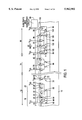
- FIG. 1 is a cross-sectional view showing a typical semiconductor device including diffusion regions, electrodes and a parasitic circuit, according to a first embodiment of the present invention.
- FIG. 2 shows a schematic pattern layout of the semiconductor device according to the first embodiment of the present invention.
- the sectional view of the electrostatic breakdown protection device 74 and the latch-up protection device 88 in FIG. 1 is sectioned at the 1--1 line shown in FIG. 2. In FIG. 2, hatching is partly used in spite of the plane pattern, so as to understand the present invention more easily.
- the semiconductor device has a substrate voltage generating circuit 80 for generating a substrate bias to be applied to a p-type substrate 10, a CMOS internal circuit 12, an electrostatic breakdown protection device (tolerance device) 74 for preventing the CMOS internal circuit 12 from being electrostatically broken down and a latch-up protection device (protection device) 88 for preventing a latch-up from occurring in the CMOS internal circuit 12.
- the detail of the CMOS circuit 12 is omitted as it is the same as that in the first comparative example.
- the tolerance device 74 is the same as the second input protection circuit 74 in the third comparative example, of which the second protection Tr 86 as the parasitic circuit is also the same as that of the third comparative example.
- the protection device 88 has an n-type first diffusion region (Nwell) 90 on the p-type substrate, which has a highly doped n-type second diffusion region (n+) 92, which is doped with more n-type impurities than the Nwell 90, and has a p-type third diffusion region 94, which is separated from the second diffusion region 92.
- An n-type fourth diffusion region (Nwell) 96 is formed at a region substantially surrounding but separated from the first diffusion region 90 on a surface of the p-type substrate 10.
- the plane pattern in FIG. 2 of the fourth diffusion region 96 looks like a quadrilateral shape surrounding the first diffusion region (Nwell) 90.
- the third diffusion region 94 is coupled with a input line.
- the second diffusion region (n+) 92 is coupled with a first supply line supplied with a supply voltage Vcc of 3.0 V.
- the fourth diffusion region (Nwell) 96 is coupled with a second supply line applied a ground voltage Vss of 0V which is supplied with through a highly doped diffusion region (n+) 98, which is doped with more doped n-type impurities than the fourth diffusion region 96.
- an internal bias generating line supplied with a substrate bias Vbb generated by the substrate bias generating circuit 80 is coupled with the p-type substrate 10 through a highly doped p-type diffusion region (p+) 34 on the outside of the protection device 88.
- the substrate bias Vbb of the p-type substrate 10 is pulled down to a lower potential than the ground voltage Vss.
- a parasitic circuit in the first embodiment will be described as follows.
- the parasitic circuits formed in the internal circuit 12 and the tolerance device 74 are the same as those of the first and second comparative examples, of which explanation is omitted.
- the third diffusion region (p+) 94, the first diffusion region (Nwell) 90 and the p-type substrate 10 respectively correspond to an emitter, a base and a collector and form an npn-type third parasitic transistor (third parasitic Tr) 100.
- the fourth diffusion region (Nwell) 96, the p-type substrate 10 and the first diffusion region (Nwell) 90 respectively correspond to an emitter, a base and a collector and form an npn-type fourth parasitic transistor (fourth parasitic Tr) 102, which is shown at two places in FIG. 1.
- the n-type diffusion region 90 including the p-type third diffusion region 94 and the second diffusion region 92, the p-type substrate 10 and the fourth diffusion region 96 form a Semiconductor Controlled Rectifier (SCR) device.
- SCR Semiconductor Controlled Rectifier
- a latch-up phenomenon and the operation of the protection device 88 will be described with reference the case where a positive surge voltage occurs at the input terminal 62 according to the first embodiment.
- the pn junction between the third diffusion region (p+) 94 and the first diffusion region (Nwell) 90 corresponds to a forward bias for the positive surge.
- the pn junction responds at the time when the potential of the third diffusion region (p+) 94 increases to a forward voltage Vf higher than that of the first diffusion region (Nwell) 90.
- the surge current can be discharged quickly to the supply voltage Vcc as the base current of the third parasitic Tr 100. Consequently, the semiconductor device according to the first embodiment can prevent a transient voltage from being applied to a gate and has a sufficient electrostatic break down tolerance without a protection resistor having large resistance.
- the transient voltage generated by the break down is described in the third comparative example.
- a part of of the surge current flows into the p-type substrate 10 as a collector current of the third parasitic Tr 100.
- the potential of the p-type substrate 10 increases to a forward voltage Vf higher than that of the fourth diffusion region 96 because of the collector current, a base-emitter junction of the fourth parasitic Tr is biased forward, and the base current flows into the fourth parasitic Tr.
- the surge current flowing into the p-type substrate is discharged to the ground voltage Vss as the base current of the fourth parasitic Tr through the highly doped diffusion region (n+) 98.
- the fourth diffusion region 96 is formed by surrounding the first diffusion region (Nwell) 90 having the third diffusion region (p+) 94, so that the surge current flowing into the p-type substrate 10 is almost completely discharged from the fourth diffusion region 96 (the current is corresponding to the current i1 in the first comparative example). Therefore, the region where the substrate potential Vbb is pulled up by the surge current is substantially limited within the region surrounded by the fourth diffusion region 96. Consequently, the semiconductor device according to the first embodiment can prevent the substrate potential of the highly doped p-type diffusion region (p+) 34 from increasing, which is coupled with the substrate bias generating circuit 80 on the outside of the protection device 88.
- the positive surge flowing from the input terminal 62 is almost completely be discharged as the current i1 within the protection device 88, and the current i2 flowing into the internal circuit 12 is reduced and the latch-up is prevented from occurring in the internal circuit 12.
- the tolerance device 74 is formed with a conventional multicollector type latch-up protection circuit so that the latch-up can be prevented from generating.
- the semiconductor device has a tolerance to the electrostatic break down and the latch-up against both positive and negative surges.
- FIG. 3 is a cross-sectional view showing a typical semiconductor device including diffusion regions, electrodes and a parasitic circuit, according to a second embodiment of the present invention.
- FIG. 4 shows a schematic pattern layout of the semiconductor device according to the second embodiment of the present invention.
- the sectional view of the electrostatic breakdown protection device 124 and the latch-up protection device 126 in FIG. 3 is sectioned at the 3--3 line shown in FIG. 4.
- field oxide films 106, electrodes and so on are omitted and the hatching is used in spite of the plane pattern, and not sectional view, so as to understand the present invention more easily.
- the semiconductor device according to the second embodiment has reversed conductivity type and reversed coupling relation between the supply voltage Vcc and the ground voltage Vss as to those of the first embodiment.
- the semiconductor device has a substrate voltage generating circuit 80 for generating a substrate bias to be applied to an n-type substrate 120, a CMOS internal circuit 122, an electrostatic breakdown protection device (tolerance device) 124 for preventing the CMOS internal circuit 122 from being electrostatically broken down and a latch-up protection device (protection device) 126 for preventing a latch-up from occurring in the CMOS internal circuit 122.
- a substrate voltage generating circuit 80 for generating a substrate bias to be applied to an n-type substrate 120
- CMOS internal circuit 122 for preventing the CMOS internal circuit 122 from being electrostatically broken down
- a latch-up protection device (protection device) 126 for preventing a latch-up from occurring in the CMOS internal circuit 122.
- NMOS Tr n-type MOS transistor 128 of the CMOS internal circuit 122 is formed in a p-type well region (Pwell) 130 on the n-type substrate 120.
- the ground voltage Vss of 0 V is applied to the drain (n+) 132 of the NMOS Tr 128 and the Pwell 130.
- the ground voltage Vss is applied to the Pwell 130 through a highly doped p-type diffusion region (p+) 136, which is doped with more doped p-type impurities than the Pwell 130.
- a p-type MOS transistor (PMOS Tr) 138 of the CMOS internal circuit 122 is formed on the n-type substrate 120.
- a supply voltage Vcc of 3.0 V is applied to the source (p+) 144 of the PMOS Tr 138.
- the supply voltage Vbb is applied to the n-type substrate 120 through a highly doped n-type diffusion region (n+) 150, which is doped with more doped n-type impurities than the n-type substrate 120.
- the tolerance device 124 has a first p-type diffusion region (p+) 146 and a second p-type diffusion region (p+) 148 on the n-type substrate 120.
- the first p-type diffusion region 148 is coupled with an input terminal through an input line.
- the supply voltage Vcc of 3.0 V is applied to the p-type diffusion region 148.
- the protection device 126 has a p-type first diffusion region (Pwell) 158 on the n-type substrate 120.
- the first diffusion region 158 has a highly doped p-type second diffusion region (p+) 160, which is doped with more doped impurities than the first diffusion region 160, and has an n-type third diffusion region (n+) 162 separated from the second diffusion region 160.
- a p-type fourth diffusion region (Pwell) 164 is formed at region substantially surrounding but separated from the first diffusion region 158 on a surface of the n-type substrate 120.
- the third diffusion region 162 is coupled with an input line.
- the second diffusion region (p+) 160 is coupled with a ground line as a first supply line and is supplied with he ground voltage Vss of 0 V.
- the fourth diffusion region (Pwell) 164 is coupled with a supply line as a second supply line and is supplied with the supply voltage Vcc of 3.0 V through a highly doped p-type diffusion region (p+) 166, which is doped with doped impurities than the fourth diffusion region 164.
- an internal potential line supplied with a substrate bias Vbb generated by the substrate bias generating circuit 80 is coupled with the n-type substrate 120 through a highly doped n-type diffusion region (n+) 150 on the outside of the protection device 126.
- the substrate bias Vbb of the n-type substrate 120 is pulled up higher than the supply voltage Vcc.
- a parasitic circuit of the second embodiment will be described as follows.
- the npn and pnp conductivity type in the parasitic circuit according to the second embodiment is reversed to that in the first embodiment.
- the drain (n+) 132 of the NMOS Tr 128 in the internal circuit 122, the Pwell 130 and the n-type substrate 120 respectively correspond to an emitter, a base and a collector and constitute an npn-type first parasitic Tr 168.
- the base of the first parasitic Tr 168 is coupled with a ground voltage through the highly doped p-type diffusion region (p+) 136 in the Pwell 130 of the internal circuit 122.
- a parasitic well resistor R1, 170 is formed between the base and the p-type highly doped diffusion region (p+) 136.
- the source (n+) 144 of the PMOS Tr 138 in the internal circuit 122, the n-type substrate 120 and the Pwell 130 respectively correspond to an emitter, a base and a collector and constitute a pnp-type second parasitic Tr 172.
- the p-type first diffusion region (p+) 146 in the tolerance device 124, the n-type substrate 120 and the p-type second diffusion region (p+) 148 respectively correspond to an emitter, a base and a collector and constitute a fifth parasitic bipolar Tr 152.
- the third diffusion region (n+) 162 in the protection device 126, the first diffusion region (Pwell) 158 and the n-type substrate 120 respectively correspond to an emitter, a base and a collector and constitute an npn-type third parasitic Tr 154.
- the fourth diffusion region (Pwell) 164, the n-type substrate 120 and the first diffusion region (Pwell) 158 correspond to a emitter, a base and a collector and constitute a pnp-type fourth parasitic Tr 156.
- the n-type third diffusion region (n+) 162, the p-type first diffusion region (Pwell) 158 including the second diffusion region (p+) 160, the n-type substrate 120 and the p-type fourth diffusion region (Pwell) 164 form a SCR device.
- the third parasitic Tr 154 and the fourth parasitic Tr 156 form a parasitic SCR (Semiconductor Controlled Rectifier).
- the pn junction between the third diffusion region (n+) 162 and the first diffusion region (Pwell) 158 corresponds to a forward bias for the negative surge.
- the pn junction responds at the time when the potential of the third diffusion region (n+) 162 decreases to a forward voltage Vf lower than that of the first diffusion region (Pwell) 158.
- the surge current can be discharged quickly to the ground voltage Vss as the base current of the third parasitic Tr 154. Consequently, the semiconductor device according to the second embodiment can prevent a transient voltage from being applied to a gate and has a sufficient electrostatic break down tolerance without a protection resistor having large resistance.
- the transient voltage due to the break down is described in the third comparative example.
- a part of of the surge current flows into the n-type substrate 120 as a collector current of the third parasitic Tr 154.
- a base-emitter junction of the fourth parasitic Tr is biased forward and the base current flows into the fourth parasitic Tr.
- the surge current flowing into the n-type substrate 120 is discharged to the supply voltage source Vcc as the base current of the fourth parasitic Tr through the highly doped diffusion region (p+) 166.
- the fourth diffusion region 164 is formed by surrounding the first diffusion region (Pwell) 158 having the third diffusion region (n+) 162, so that the surge current flowing into the n-type substrate 120 is almost completely discharged from the fourth diffusion region 164 (the current corresponds to the current i1 in the first comparative example). Therefore, the region where the substrate potential Vbb is pulled down by the surge current is substantially limited within the region surrounded by the fourth diffusion region 164. Consequently, the semiconductor device according to the second embodiment can prevent the substrate potential of the highly doped n-type diffusion region (n+) 150 from decreasing, which is coupled with the substrate bias generating circuit 80 on the outside of the protection device 126.
- the negative surge flowing from the input terminal 62 can almost completely be discharged as the current i1 within the protection device 126, so that the current i2 flowing into the internal circuit 122 can be reduced and the latch-up can be prevented from occurring in the internal circuit 122.
- the positive surge flowing from the input terminal 62 flows into the semiconductor device through the p-type first diffusion region (p+) 146 of the tolerance device 124.
- the direction of the positive surge corresponds to a forward bias for the base-emitter junction of the fifth parasitic Tr 152.
- the fifth parasitic Tr 152 is turned on by the positive surge at the time when the potential of the p-type first diffusion region (p+) 146 increases to a forward voltage Vf higher than that of the n-type substrate 120. Then, the surge current can be discharged quickly to a supply voltage source Vcc in FIG. 3 as the collector current of the fifth parasitic Tr 152. Consequently, the semiconductor device according to the second embodiment can achieve sufficient tolerance. Further the tolerance device is formed with a conventional multicollector typelatch-up protection circuit so that the latch-up can be prevented from occurring when a positive surge occurs.
- the semiconductor device has a tolerance of the electrostatic break down and the latch-up against both positive and negative surges.
- FIG. 5 is a cross-sectional view showing a typical semiconductor device including diffusion regions, electrodes and a parasitic circuit, according to a third embodiment of the present invention.
- FIG. 6 shows a schematic pattern layout of the semiconductor device according to the third embodiment of the present invention.
- the sectional view of the electrostatic breakdown protection device 74 and the latch-up protection device 88 in FIG. 5 is sectioned at the 5--5 line shown in FIG. 6.
- field oxide films 106, electrodes and so on are omitted and the hatching is partly used in spite of the plane pattern, and not sectional view, so as to understand the present invention more easily.
- the semiconductor device according to the third embodiment has the same structure as the semiconductor device according to the first embodiment, except for a gate electrode 174 of a MOS Tr on a gate oxide film (not shown in FIG. 5) on a first diffusion region 90 between a second diffusion region 92 and a third diffusion region 94 in the protection device 88.
- the same parts in the third embodiment as in the first embodiment are shown with the same reference characters, and their explanations are omitted. An explanation of an operation of the third embodiment for the case of a surge voltage occurring is omitted because it is the same as that of the first embodiment.
- the second diffusion region 92 and the third diffusion region 94 perform like a source and a drain of a MOS Tr.
- a supply voltage Vcc of 3.0 V is applied to the gate electrode 174.
- the channel under the gate electrode 174 is kept closed (off). Consequently, the second diffusion region 92 and the third diffusion region 94 are separated from each other by the gate electrode 174.
- the distance between the second diffusion region 92 and the third diffusion region 94 can be shorter than that for the case of the field oxide film 106, which is formed according to the first embodiment. Consequently, the area occupied by the latch-up protection device can be reduced.
- FIG. 7 is a cross-sectional view showing a typical semiconductor device including diffusion regions, electrodes and a parasitic circuit, according to a fourth embodiment of the present invention.
- FIG. 8 shows a schematic pattern layout of the semiconductor device according to the fourth embodiment of the present invention.
- the sectional view of the electrostatic breakdown protection device 124 and the latch-up protection device 126 in FIG. 7 is sectioned at the 7--7 line shown in FIG. 8.
- field oxide films 106, electrodes and so on are omitted and the hatching is partly used in spite of the plane pattern, and not the sectional view, so as to understand the present invention more easily.
- the semiconductor device according to the fourth embodiment has the same structure as the semiconductor device according to the second embodiment except for a gate electrode 174 of a MOS Tr on a gate oxide film (not shown in FIG. 7) on a first diffusion region 158 between a second diffusion region 160 and a third diffusion region 162 in the protection device 126.
- the same parts in the fourth embodiment as in the second embodiment are shown with the same reference characters and their explanations are omitted. An explanation of an operation of the fourth embodiment for the case of a surge voltage occurring is omitted because it is the same as that of the second embodiment.
- the second diffusion region 160 and the third diffusion region 162 respectively, have similar structure to a source and a drain of a MOS Tr.
- a ground voltage Vss of 0 V is applied to the gate electrode 174.
- the channel under the gate electrode 174 is kept closed (off), so that the second diffusion region 160 and the third diffusion region 162 are separated by the gate electrode 174 from each other.
- the distance between the second diffusion region 160 and the third diffusion region 162 can be shorter than that for the case of the field oxide film 106 is formed according to the first embodiment. Consequently, the area occupied by the latch-up protection device can be reduced.
- FIG. 9 is a cross-sectional view showing a typical semiconductor device including diffusion regions, electrodes and a parasitic circuit, according to a fifth embodiment of the present invention.
- FIG. 10 shows a schematic pattern layout of the semiconductor device according to the fifth embodiment of the present invention.
- the sectional view of the tolerance device 74 and the protection device 88 in FIG. 9 is sectioned at the 9--9 line shown in FIG. 10.
- field oxide films 106, electrodes and so on are omitted, and the hatching is used in spite of the plane pattern, and not sectional view, so as to understand the present invention more easily.
- the semiconductor device according to the fifth embodiment has the same structure as the semiconductor device according to the first embodiment, except for the fourth diffusion region 96 in the protection device 88, which performs as a collector an npn-type parasitic bipolar Tr.
- the same parts in the fifth embodiment as in the first embodiment are shown with the same reference characters, and their explanations are omitted. An explanation of an operation of the fifth embodiment for the case of a surge voltage occurring is omitted because it is the same as that for the first embodiment.
- the fourth diffusion region 96 in the protection device 88 which is coupled with a ground voltage source Vss through the highly doped diffusion region 98, also performs as the second n-type diffusion region 82 in the tolerance device 74 according to the first embodiment shown in FIG. 1.
- the first n-type diffusion region 76, the p-type substrate 10 and the fourth diffusion region 96 respectively correspond to an emitter, a base and a collector and form an npn-type parasitic bipolar Tr 86a.
- a negative surge flowing from an input terminal corresponds to a forward bias for the parasitic bipolar Tr 86a. Consequently, the parasitic bipolar Tr 86a serves the same function as the tolerance device 74.
- the fourth diffusion region 96 serves both as a part of the protection device 88 and as the second n-type diffusion region 82 of the tolerance device 74 in the first embodiment. Consequently, the area occupied by the protection device and the tolerance device can be reduced to an area smaller than that of the semiconductor device according to the first embodiment, while keeping the latch-up tolerance and the electrostatic break down tolerance.
- FIG. 11 is a cross-sectional view showing a typical semiconductor device including diffusion regions, electrodes and a parasitic circuit, according to a sixth embodiment of the present invention.
- FIG. 12 shows a schematic pattern layout of the semiconductor device according to the sixth embodiment of the present invention.
- the sectional view of the electrostatic breakdown protection device 124 and the latch-up protection device 126 in FIG. 10 is sectioned at the 11--11 line shown in FIG. 12.
- field oxide films 106, electrodes and so on are omitted and the hatching is used in spite of the plane pattern, and not sectional view, so as to understand the present invention more easily.
- the semiconductor device according to the sixth embodiment has the same structure as the semiconductor device according to the second embodiment, except for the fourth diffusion region 164 in the protection device 126, which performs as a collector in a pnp-type parasitic bipolar Tr.
- the same parts in the sixth embodiment as those in the second embodiment are shown with the same reference characters and their explanations are omitted. An explanation of the operation of the sixth embodiment for the case of a surge voltage occurring is omitted because it is the same as that of the second embodiment.
- the fourth diffusion region 164 in the protection device 126 which is coupled with a supply voltage source Vcc through the highly doped diffusion region 166, also performs as the second p-type diffusion region 148 in the tolerance device 124 according to the second embodiment shown in FIG. 3.
- the first p-type diffusion region 146, the n-type substrate 120 and the fourth diffusion region 164 respectively correspond to an emitter, a base and a collector and form an pnp-type parasitic bipolar Tr 152a.
- a positive surge flowing from an input terminal corresponds to a forward bias for the parasitic bipolar Tr 152a. Consequently, the parasitic bipolar Tr 152a serves the same function as the tolerance device 124.
- the fourth diffusion region 164 serves both as a part of the protection device 126 and as the second p-type diffusion region 148 of the tolerance device 124 in the second embodiment. Consequently, the area occupied by the protection device and the tolerance device can be reduced to an area smaller than that of the semiconductor device according to the second embodiment, while keeping the latch-up tolerance and the electrostatic break down tolerance.
- FIGS. 14 and 15 a seventh preferred embodiment of the semiconductor devices according to the present invention is shown.
- FIG. 13 shows a schematic pattern layout of the semiconductor device according to the seventh embodiment of the present invention.
- field oxide films 106 and so on are omitted so as to understand the present invention more easily.
- FIG. 14 is a cross-sectional view showing a typical semiconductor device including diffusion regions, electrodes and a parasitic circuit, according to a seventh embodiment of the present invention, sectioned at the 14--14 line shown in FIG. 13.
- FIG. 15 is a cross-sectional view showing a typical semiconductor device including diffusion regions and electrodes according to a seventh embodiment of the present invention, sectioned at the 15--15 line shown in FIG. 13.
- the semiconductor device according to the seventh embodiment has the same structure as the semiconductor device according to the first embodiment, except for a resistor for preventing an electrostatic break down which is formed with a part of the third diffusion region in the protection device 88 (See FIG. 1).
- the same parts in the seventh embodiment as in the first embodiment are shown with the same reference characters, and their explanations are omitted. An explanation of the operation of the seventh embodiment for the case of a surge voltage occurs is omitted because it is the same as that of the first embodiment.
- a control line 180 electrically coupled with a gate electrode in a CMOS internal circuit is electrically coupled with the third diffusion region 94 in the protection device 88.
- the control line (metallic line for coupling gates) 180 is coupled with the third diffusion region 94 through a first coupling hole 182.
- the third diffusion region 94 is electrically coupled with an input line 184 coupled with an input terminal through a second coupling hole 186.
- a part of the third diffusion region 94 between the first coupling hole 182 and the second coupling hole 186 is used as the resistor for preventing an electrostatic break down (input protection resistor) 188 as shown in FIG. 15.
- the input protection resistor 188 has the simplest structure and acts as a resistor for preventing the electrostatic break down.
- the input protection resistor 188 delays the application of a positive surge to the gate oxide film in the CMOS internal circuit.
- the delay time of the input protection resistor 188 can be adjusted by changing the size of the input protection resistor 188 so as not to affect a normal signal transmission of a semiconductor device.
- metal lines 190 and 192 are for coupling with a ground voltage source Vss and a supply voltage source Vcc, respectively.
- the metal line 190 for coupling with the Vss is coupled with the fourth diffusion region 98 through a coupling hole 196 holed through an insulating layer 194.
- the metal line 192 for coupling with the Vcc is coupled with the second diffusion region 92 through a coupling hole 196 holed through an insulating layer 194.
- a surface protection layer 198 is formed on the surface.
- the semiconductor device according to the seventh embodiment shown in FIG. 14 has a third parasitic Tr 100 and a fourth parasitic Tr 102.
- the semiconductor device according to the seventh embodiment has a device for preventing the electrostatic break down in the protection device 88 so that the input protection resistor 188 prevents itself from being a new source of a latch-up trigger current.
- both the third diffusion region 94 in the protection device 88 are identical to both the third diffusion region 94 in the protection device 88.
- the semiconductor device has an electrostatic break down tolerance without reducing a latch-up tolerance.
- FIG. 16 shows a schematic pattern layout of the semiconductor device according to the eighth embodiment of the present invention.
- field oxide films 106 and so on are omitted so as to understand the present invention more easily.
- FIG. 17 is a cross-sectional view showing a typical semiconductor device including diffusion regions, electrodes and a parasitic circuit, according to an eighth embodiment of the present invention, sectioned at the 17--17 line shown in FIG. 16.
- FIG. 18 is a cross-sectional view showing a typical semiconductor device including diffusion regions and electrodes according to an eighth embodiment of the present invention, sectioned at the 18--18 line shown in FIG. 16.
- the semiconductor device according to the eighth embodiment has the same structure as the semiconductor device according to the second embodiment, except for a resistor for preventing an electrostatic break down which is formed with a part of the third diffusion region 162 in the protection device 126 (See FIG. 3).
- the same parts in the eighth embodiment as in the second embodiment are shown with the same reference characters, and their explanations are omitted. An explanation of the operation of the eighth embodiment for the case of a surge voltage occurring is omitted because it is the same as that of the second embodiment.
- a control line 180 electrically coupled with a gate electrode in a CMOS internal circuit is electrically coupled with the third diffusion region 162 in the protection device 126.
- the control line (metallic line for coupling gates) 180 is coupled with the third diffusion region 162 through a first coupling hole 182.
- the third diffusion region 162 is electrically coupled with an input line 184 coupled with an input terminal through a second coupling hole 186.
- a part of the third diffusion region 162 between the first coupling hole 182 and the second coupling hole 186 is used as the resistor for preventing an electrostatic break down (input protection resistor) 188 as shown in FIG. 18.
- the input protection resistor 188 has the simplest structure and acts as a resistor for preventing the electrostatic break down.
- the input protection resistor 188 delays the application of a positive surge to the gate oxide film in the CMOS internal circuit.
- the delay time of the input protection resistor 188 is adjustable by changing the size of the input protection resistor 188 so as not to affect a normal signal transmission of a semiconductor device.
- metal lines 190 and 192 are for coupling with a ground voltage source Vss and a supply voltage source Vcc.
- the metal line 190 for coupling with the Vss is coupled with the second diffusion region 160 through a coupling hole 196 holed through an insulating layer 194.
- the metal line 192 for coupling with the Vcc is coupled with the fourth diffusion region 166 through a coupling hole 196 holed through an insulating layer 194.
- a surface protection layer 198 is formed on the surface.
- the semiconductor device according to the eighth embodiment shown in FIG. 17 has a third parasitic Tr 154 and a fourth parasitic Tr 156.
- the semiconductor device according to the eighth embodiment has a device for preventing the electrostatic break down in the protection device 126 so that the input protection resistor 188 prevents itself from being a new source of a latch-up trigger current.
- both the third diffusion region 162 in the protection device 126 are identical to both the third diffusion region 162 in the protection device 126.
- the semiconductor device has an electrostatic break down tolerance without reducing a latch-up tolerance.
- the fourth diffusion region which is formed by surrounding the whole first diffusion region on the surface of the substrate, does not need to be formed by surrounding the whole diffusion region but may be formed by a plane pattern having a "U" shape.
- the present invention provides a semiconductor device which allows surge to flow from an input line to a first or second supply voltage source line through the SCR, which is the parasitic bipolar Tr in the protection device. Consequently, the semiconductor device reduces the surge flowing into a CMOS internal circuit and has a latch-up tolerance and an electrostatic break down tolerance without delaying operation speed. Moreover, the area occupied by the protection device can be reduced because the distance between the second and third diffusion regions, which is separated by a gate electrode, can be shorter than the distance separated by a field oxide film.
Landscapes
- Engineering & Computer Science (AREA)
- Power Engineering (AREA)
- Physics & Mathematics (AREA)
- Condensed Matter Physics & Semiconductors (AREA)
- General Physics & Mathematics (AREA)
- Computer Hardware Design (AREA)
- Microelectronics & Electronic Packaging (AREA)
- Semiconductor Integrated Circuits (AREA)
- Metal-Oxide And Bipolar Metal-Oxide Semiconductor Integrated Circuits (AREA)
- Static Random-Access Memory (AREA)
Applications Claiming Priority (2)
| Application Number | Priority Date | Filing Date | Title |
|---|---|---|---|
| JP8-220079 | 1996-08-21 | ||
| JP8220079A JPH1065020A (ja) | 1996-08-21 | 1996-08-21 | 半導体装置 |
Publications (1)
| Publication Number | Publication Date |
|---|---|
| US5962902A true US5962902A (en) | 1999-10-05 |
Family
ID=16745611
Family Applications (1)
| Application Number | Title | Priority Date | Filing Date |
|---|---|---|---|
| US08/915,325 Expired - Fee Related US5962902A (en) | 1996-08-21 | 1997-08-20 | Semiconductor CMOS device with circuit for preventing latch-up |
Country Status (6)
| Country | Link |
|---|---|
| US (1) | US5962902A (ko) |
| EP (1) | EP0827206B1 (ko) |
| JP (1) | JPH1065020A (ko) |
| KR (1) | KR100336154B1 (ko) |
| DE (1) | DE69733388T2 (ko) |
| TW (1) | TW334625B (ko) |
Cited By (11)
| Publication number | Priority date | Publication date | Assignee | Title |
|---|---|---|---|---|
| US6137143A (en) * | 1998-06-30 | 2000-10-24 | Intel Corporation | Diode and transistor design for high speed I/O |
| US6320229B1 (en) * | 1998-05-18 | 2001-11-20 | Matsushita Electronics Corporation | Semiconductor device |
| US6407898B1 (en) * | 2000-01-18 | 2002-06-18 | Taiwan Semiconductor Manufacturing Company Ltd. | Protection means for preventing power-on sequence induced latch-up |
| US20050286295A1 (en) * | 2004-06-25 | 2005-12-29 | Kapre Ravindra M | Memory cell array latchup prevention |
| US20070080430A1 (en) * | 2005-10-07 | 2007-04-12 | Nec Electronics Corporation | Semiconductor device |
| US20080198519A1 (en) * | 2007-02-15 | 2008-08-21 | Lim Dong Ju | Electrostatic discharge protection element having an improved area efficiency |
| US20110042747A1 (en) * | 2009-08-24 | 2011-02-24 | Stmicroelectronics S.A. | Structure for protecting an integrated circuit against electrostatic discharges |
| US20120108045A1 (en) * | 2004-02-17 | 2012-05-03 | Morris Wesley H | Method for radiation hardening a semiconductor device |
| US8278684B1 (en) * | 2007-12-12 | 2012-10-02 | Cypress Semiconductor Corporation | Voltage protection device |
| US9842629B2 (en) | 2004-06-25 | 2017-12-12 | Cypress Semiconductor Corporation | Memory cell array latchup prevention |
| US10038058B2 (en) | 2016-05-07 | 2018-07-31 | Silicon Space Technology Corporation | FinFET device structure and method for forming same |
Families Citing this family (4)
| Publication number | Priority date | Publication date | Assignee | Title |
|---|---|---|---|---|
| JP3348782B2 (ja) | 1999-07-22 | 2002-11-20 | 日本電気株式会社 | 半導体装置の製造方法 |
| JP2006269902A (ja) * | 2005-03-25 | 2006-10-05 | Oki Electric Ind Co Ltd | 半導体集積回路 |
| DE602007005289D1 (de) | 2006-01-24 | 2010-04-29 | St Microelectronics Sa | Schutzschaltung für eine integrierte Schaltung gegen parasitäre latch-up Phänomene |
| JP7048160B2 (ja) * | 2021-01-13 | 2022-04-05 | ラピスセミコンダクタ株式会社 | 半導体装置 |
Citations (8)
| Publication number | Priority date | Publication date | Assignee | Title |
|---|---|---|---|---|
| US4476476A (en) * | 1979-04-05 | 1984-10-09 | National Semiconductor Corporation | CMOS Input and output protection circuit |
| JPS6118315A (ja) * | 1984-06-14 | 1986-01-27 | テキサス インスツルメンツ ドイツエランド ゲゼルシヤフト ミツト ベシユレンクテル ハフツング | 保護回路装置 |
| US4647956A (en) * | 1985-02-12 | 1987-03-03 | Cypress Semiconductor Corp. | Back biased CMOS device with means for eliminating latchup |
| US4870530A (en) * | 1988-06-27 | 1989-09-26 | Advanced Micro Devices, Inc. | Electrostatic discharge protection circuitry for any two external pins of an I.C. package |
| JPH04247654A (ja) * | 1991-02-04 | 1992-09-03 | Nissan Motor Co Ltd | 入出力保護回路 |
| JPH04324641A (ja) * | 1991-04-24 | 1992-11-13 | Sanyo Electric Co Ltd | 半導体集積回路 |
| US5468984A (en) * | 1994-11-02 | 1995-11-21 | Texas Instruments Incorporated | ESD protection structure using LDMOS diodes with thick copper interconnect |
| US5629544A (en) * | 1995-04-25 | 1997-05-13 | International Business Machines Corporation | Semiconductor diode with silicide films and trench isolation |
-
1996
- 1996-08-21 JP JP8220079A patent/JPH1065020A/ja not_active Withdrawn
-
1997
- 1997-08-05 TW TW086111162A patent/TW334625B/zh not_active IP Right Cessation
- 1997-08-20 EP EP97114366A patent/EP0827206B1/en not_active Expired - Lifetime
- 1997-08-20 KR KR1019970039624A patent/KR100336154B1/ko not_active IP Right Cessation
- 1997-08-20 DE DE69733388T patent/DE69733388T2/de not_active Expired - Lifetime
- 1997-08-20 US US08/915,325 patent/US5962902A/en not_active Expired - Fee Related
Patent Citations (10)
| Publication number | Priority date | Publication date | Assignee | Title |
|---|---|---|---|---|
| US4476476A (en) * | 1979-04-05 | 1984-10-09 | National Semiconductor Corporation | CMOS Input and output protection circuit |
| JPS6118315A (ja) * | 1984-06-14 | 1986-01-27 | テキサス インスツルメンツ ドイツエランド ゲゼルシヤフト ミツト ベシユレンクテル ハフツング | 保護回路装置 |
| US4686602A (en) * | 1984-06-14 | 1987-08-11 | Texas Instruments Incorporated | Protective circuit arrangement for protecting semiconductor components |
| US4647956A (en) * | 1985-02-12 | 1987-03-03 | Cypress Semiconductor Corp. | Back biased CMOS device with means for eliminating latchup |
| US4870530A (en) * | 1988-06-27 | 1989-09-26 | Advanced Micro Devices, Inc. | Electrostatic discharge protection circuitry for any two external pins of an I.C. package |
| JPH02119169A (ja) * | 1988-06-27 | 1990-05-07 | Advanced Micro Devices Inc | 保護回路 |
| JPH04247654A (ja) * | 1991-02-04 | 1992-09-03 | Nissan Motor Co Ltd | 入出力保護回路 |
| JPH04324641A (ja) * | 1991-04-24 | 1992-11-13 | Sanyo Electric Co Ltd | 半導体集積回路 |
| US5468984A (en) * | 1994-11-02 | 1995-11-21 | Texas Instruments Incorporated | ESD protection structure using LDMOS diodes with thick copper interconnect |
| US5629544A (en) * | 1995-04-25 | 1997-05-13 | International Business Machines Corporation | Semiconductor diode with silicide films and trench isolation |
Cited By (20)
| Publication number | Priority date | Publication date | Assignee | Title |
|---|---|---|---|---|
| US6320229B1 (en) * | 1998-05-18 | 2001-11-20 | Matsushita Electronics Corporation | Semiconductor device |
| US6137143A (en) * | 1998-06-30 | 2000-10-24 | Intel Corporation | Diode and transistor design for high speed I/O |
| US6407898B1 (en) * | 2000-01-18 | 2002-06-18 | Taiwan Semiconductor Manufacturing Company Ltd. | Protection means for preventing power-on sequence induced latch-up |
| US20120108045A1 (en) * | 2004-02-17 | 2012-05-03 | Morris Wesley H | Method for radiation hardening a semiconductor device |
| US8497195B2 (en) * | 2004-02-17 | 2013-07-30 | Silicon Space Technology Corporation | Method for radiation hardening a semiconductor device |
| US9842629B2 (en) | 2004-06-25 | 2017-12-12 | Cypress Semiconductor Corporation | Memory cell array latchup prevention |
| US20090213677A1 (en) * | 2004-06-25 | 2009-08-27 | Kapre Ravindra M | Memory Cell Array |
| US7773442B2 (en) * | 2004-06-25 | 2010-08-10 | Cypress Semiconductor Corporation | Memory cell array latchup prevention |
| US8045410B2 (en) | 2004-06-25 | 2011-10-25 | Cypress Semiconductor Corporation | Memory cell array |
| US20050286295A1 (en) * | 2004-06-25 | 2005-12-29 | Kapre Ravindra M | Memory cell array latchup prevention |
| US8837245B2 (en) | 2004-06-25 | 2014-09-16 | Cypress Semiconductor Corporation | Memory cell array latchup prevention |
| US8493804B2 (en) | 2004-06-25 | 2013-07-23 | Cypress Semiconductor Corporation | Memory cell array latchup prevention |
| US7514766B2 (en) * | 2005-10-07 | 2009-04-07 | Nec Electronics Corporation | Semiconductor device |
| US20070080430A1 (en) * | 2005-10-07 | 2007-04-12 | Nec Electronics Corporation | Semiconductor device |
| US20080198519A1 (en) * | 2007-02-15 | 2008-08-21 | Lim Dong Ju | Electrostatic discharge protection element having an improved area efficiency |
| US8278684B1 (en) * | 2007-12-12 | 2012-10-02 | Cypress Semiconductor Corporation | Voltage protection device |
| US8610216B2 (en) * | 2009-08-24 | 2013-12-17 | Stmicroelectronics S.A. | Structure for protecting an integrated circuit against electrostatic discharges |
| US20110042747A1 (en) * | 2009-08-24 | 2011-02-24 | Stmicroelectronics S.A. | Structure for protecting an integrated circuit against electrostatic discharges |
| US10038058B2 (en) | 2016-05-07 | 2018-07-31 | Silicon Space Technology Corporation | FinFET device structure and method for forming same |
| US10615260B1 (en) | 2016-05-07 | 2020-04-07 | Silicon Space Technology Corporation | Method for forming FinFET device structure |
Also Published As
| Publication number | Publication date |
|---|---|
| EP0827206B1 (en) | 2005-06-01 |
| JPH1065020A (ja) | 1998-03-06 |
| DE69733388T2 (de) | 2006-04-27 |
| TW334625B (en) | 1998-06-21 |
| EP0827206A3 (en) | 1998-04-01 |
| DE69733388D1 (de) | 2005-07-07 |
| EP0827206A2 (en) | 1998-03-04 |
| KR100336154B1 (ko) | 2002-06-20 |
| KR19980018812A (ko) | 1998-06-05 |
Similar Documents
| Publication | Publication Date | Title |
|---|---|---|
| JP3058203U (ja) | ラッチアップのない完全に保護されたcmosオンチップesd保護回路 | |
| KR100441116B1 (ko) | 낮은 트리거 전압에서 동작 가능한 반도체-제어 정류기구조의 정전 방전 보호 회로 | |
| TWI462267B (zh) | 可提供低電壓電路保護之金氧半(mos)電晶體觸發暫態電壓抑制器 | |
| US6236087B1 (en) | SCR cell for electrical overstress protection of electronic circuits | |
| US5962902A (en) | Semiconductor CMOS device with circuit for preventing latch-up | |
| US8039899B2 (en) | Electrostatic discharge protection device | |
| US4672584A (en) | CMOS integrated circuit | |
| US6072219A (en) | Substrate-triggering electrostatic discharge protection circuit for deep-submicron integrated circuits | |
| EP0776092B1 (en) | Semiconductor device | |
| US5760446A (en) | Electrostatic discharge structure of semiconductor device | |
| US20060232898A1 (en) | ESD protection circuit with SCR structure for semiconductor device | |
| US5675469A (en) | Integrated circuit with electrostatic discharge (ESD) protection and ESD protection circuit | |
| US5747837A (en) | Semiconductor device having input protective function | |
| US20040257728A1 (en) | Electrostatic discharge protection device and network with high voltage tolerance | |
| TWI784502B (zh) | 靜電放電防護電路 | |
| JP3320872B2 (ja) | Cmos集積回路装置 | |
| KR100750588B1 (ko) | 정전기 방전 보호회로 | |
| KR100379286B1 (ko) | 보호 회로를 구비한 반도체 장치 | |
| US7782579B2 (en) | Semiconductor integrated circuit | |
| KR20040090480A (ko) | 내부 회로를 보호하는 보호 회로를 구비한 반도체 장치 | |
| US6707653B2 (en) | Semiconductor controlled rectifier for use in electrostatic discharge protection circuit | |
| US5892263A (en) | CMOS device connected to at least three power supplies for preventing latch-up | |
| JP3131525B2 (ja) | Mosパワー・トランジスタ・デバイス | |
| US5767537A (en) | Capacitively triggered silicon controlled rectifier circuit | |
| US6084272A (en) | Electrostatic discharge protective circuit for semiconductor device |
Legal Events
| Date | Code | Title | Description |
|---|---|---|---|
| AS | Assignment |
Owner name: OKI ELECTRIC INDUSTRY CO., LTD., JAPAN Free format text: ASSIGNMENT OF ASSIGNORS INTEREST;ASSIGNORS:KATO, KATSUHIRO;KIKUCHI, HIDEKAZU;REEL/FRAME:009616/0451 Effective date: 19970827 |
|
| FEPP | Fee payment procedure |
Free format text: PAYOR NUMBER ASSIGNED (ORIGINAL EVENT CODE: ASPN); ENTITY STATUS OF PATENT OWNER: LARGE ENTITY |
|
| FPAY | Fee payment |
Year of fee payment: 4 |
|
| FPAY | Fee payment |
Year of fee payment: 8 |
|
| AS | Assignment |
Owner name: OKI SEMICONDUCTOR CO., LTD., JAPAN Free format text: CHANGE OF NAME;ASSIGNOR:OKI ELECTRIC INDUSTRY CO., LTD.;REEL/FRAME:022288/0277 Effective date: 20081001 |
|
| REMI | Maintenance fee reminder mailed | ||
| LAPS | Lapse for failure to pay maintenance fees | ||
| STCH | Information on status: patent discontinuation |
Free format text: PATENT EXPIRED DUE TO NONPAYMENT OF MAINTENANCE FEES UNDER 37 CFR 1.362 |
|
| FP | Lapsed due to failure to pay maintenance fee |
Effective date: 20111005 |