US5903036A - Semiconductor device having MISFET SRAM cells in which active regions and gate electrodes are dimensioned for increasing storage node capacitances without increasing memory cell size - Google Patents
Semiconductor device having MISFET SRAM cells in which active regions and gate electrodes are dimensioned for increasing storage node capacitances without increasing memory cell size Download PDFInfo
- Publication number
- US5903036A US5903036A US08/820,247 US82024797A US5903036A US 5903036 A US5903036 A US 5903036A US 82024797 A US82024797 A US 82024797A US 5903036 A US5903036 A US 5903036A
- Authority
- US
- United States
- Prior art keywords
- misfet
- gate electrode
- driver
- gate
- misfets
- Prior art date
- Legal status (The legal status is an assumption and is not a legal conclusion. Google has not performed a legal analysis and makes no representation as to the accuracy of the status listed.)
- Expired - Lifetime
Links
Images


Classifications
-
- H—ELECTRICITY
- H01—ELECTRIC ELEMENTS
- H01L—SEMICONDUCTOR DEVICES NOT COVERED BY CLASS H10
- H01L21/00—Processes or apparatus adapted for the manufacture or treatment of semiconductor or solid state devices or of parts thereof
- H01L21/70—Manufacture or treatment of devices consisting of a plurality of solid state components formed in or on a common substrate or of parts thereof; Manufacture of integrated circuit devices or of parts thereof
- H01L21/77—Manufacture or treatment of devices consisting of a plurality of solid state components or integrated circuits formed in, or on, a common substrate
- H01L21/78—Manufacture or treatment of devices consisting of a plurality of solid state components or integrated circuits formed in, or on, a common substrate with subsequent division of the substrate into plural individual devices
- H01L21/82—Manufacture or treatment of devices consisting of a plurality of solid state components or integrated circuits formed in, or on, a common substrate with subsequent division of the substrate into plural individual devices to produce devices, e.g. integrated circuits, each consisting of a plurality of components
- H01L21/822—Manufacture or treatment of devices consisting of a plurality of solid state components or integrated circuits formed in, or on, a common substrate with subsequent division of the substrate into plural individual devices to produce devices, e.g. integrated circuits, each consisting of a plurality of components the substrate being a semiconductor, using silicon technology
- H01L21/8232—Field-effect technology
- H01L21/8234—MIS technology, i.e. integration processes of field effect transistors of the conductor-insulator-semiconductor type
- H01L21/823418—MIS technology, i.e. integration processes of field effect transistors of the conductor-insulator-semiconductor type with a particular manufacturing method of the source or drain structures, e.g. specific source or drain implants or silicided source or drain structures or raised source or drain structures
-
- H—ELECTRICITY
- H01—ELECTRIC ELEMENTS
- H01L—SEMICONDUCTOR DEVICES NOT COVERED BY CLASS H10
- H01L21/00—Processes or apparatus adapted for the manufacture or treatment of semiconductor or solid state devices or of parts thereof
- H01L21/70—Manufacture or treatment of devices consisting of a plurality of solid state components formed in or on a common substrate or of parts thereof; Manufacture of integrated circuit devices or of parts thereof
- H01L21/77—Manufacture or treatment of devices consisting of a plurality of solid state components or integrated circuits formed in, or on, a common substrate
- H01L21/78—Manufacture or treatment of devices consisting of a plurality of solid state components or integrated circuits formed in, or on, a common substrate with subsequent division of the substrate into plural individual devices
- H01L21/82—Manufacture or treatment of devices consisting of a plurality of solid state components or integrated circuits formed in, or on, a common substrate with subsequent division of the substrate into plural individual devices to produce devices, e.g. integrated circuits, each consisting of a plurality of components
- H01L21/822—Manufacture or treatment of devices consisting of a plurality of solid state components or integrated circuits formed in, or on, a common substrate with subsequent division of the substrate into plural individual devices to produce devices, e.g. integrated circuits, each consisting of a plurality of components the substrate being a semiconductor, using silicon technology
- H01L21/8232—Field-effect technology
- H01L21/8234—MIS technology, i.e. integration processes of field effect transistors of the conductor-insulator-semiconductor type
- H01L21/823437—MIS technology, i.e. integration processes of field effect transistors of the conductor-insulator-semiconductor type with a particular manufacturing method of the gate conductors, e.g. particular materials, shapes
- H01L21/823456—MIS technology, i.e. integration processes of field effect transistors of the conductor-insulator-semiconductor type with a particular manufacturing method of the gate conductors, e.g. particular materials, shapes gate conductors with different shapes, lengths or dimensions
-
- H—ELECTRICITY
- H10—SEMICONDUCTOR DEVICES; ELECTRIC SOLID-STATE DEVICES NOT OTHERWISE PROVIDED FOR
- H10B—ELECTRONIC MEMORY DEVICES
- H10B10/00—Static random access memory [SRAM] devices
-
- H—ELECTRICITY
- H10—SEMICONDUCTOR DEVICES; ELECTRIC SOLID-STATE DEVICES NOT OTHERWISE PROVIDED FOR
- H10B—ELECTRONIC MEMORY DEVICES
- H10B10/00—Static random access memory [SRAM] devices
- H10B10/15—Static random access memory [SRAM] devices comprising a resistor load element
-
- Y—GENERAL TAGGING OF NEW TECHNOLOGICAL DEVELOPMENTS; GENERAL TAGGING OF CROSS-SECTIONAL TECHNOLOGIES SPANNING OVER SEVERAL SECTIONS OF THE IPC; TECHNICAL SUBJECTS COVERED BY FORMER USPC CROSS-REFERENCE ART COLLECTIONS [XRACs] AND DIGESTS
- Y10—TECHNICAL SUBJECTS COVERED BY FORMER USPC
- Y10S—TECHNICAL SUBJECTS COVERED BY FORMER USPC CROSS-REFERENCE ART COLLECTIONS [XRACs] AND DIGESTS
- Y10S257/00—Active solid-state devices, e.g. transistors, solid-state diodes
- Y10S257/903—FET configuration adapted for use as static memory cell
Definitions
- the present invention relates to a semiconductor integrated circuit device and, more particularly, to improvements applied advantageously to a semiconductor integrated circuit device having an SRAM (static random access memory).
- SRAM static random access memory
- the general SRAM chip layout is composed of memory cell arrays for holding data.
- word drivers i.e., pre-decoders and Y-switches, i.e., direct peripheral circuits that select appropriate memory cells when data is written or read thereto or therefrom.
- Y-switches i.e., direct peripheral circuits that select appropriate memory cells when data is written or read thereto or therefrom.
- input and output buffers i.e., peripheral circuits for controlling actual circuit operations.
- peripheral circuits for controlling actual circuit operations.
- the memory cells in the above-mentioned memory cell arrays are of one of two types: high resistance load type, and complete CMOS (complementary metal oxide semiconductor) type.
- the high resistance load type memory cell combines resistor elements with n-channel MISFETs (metal insulator semiconductor field effect transistors); the complete CMOS type memory cell combines n-channel MISFETs with p-channel MISFETs. These memory cells are designed for high degrees of integration and high yield in fabrication.
- CMOS SRAM is used as the main memory for systems for which low costs are emphasized, such as mainframe computers and workstations.
- the CMOS SRAM combines high resistance load type or complete CMOS type memory cells with peripheral circuits composed of MISFETs.
- the cache memory is made up of what is known as a bipolar CMOS SRAM.
- the bipolar CMOS SRAM combines high resistance load type or complete CMOS type memory cells with peripheral circuits composed of bipolar transistors and CMOSFETs.
- IEDM International Electron Device Meeting
- Tech. Dig. pp. 447-480, 1991.
- a high resistance load type memory cell of the SRAM typically comprises a pair of driver MISFETs Qd 1 and Qd 2 , a pair of resistor elements (load elements) R1 and R2, a pair of transistor MISFETs Qt 1 and Qt 2 , a pair of complementary data lines (DL, bar DL), and a pair of word lines WL 1 and WL 2 .
- the driver MISFETs Qd 1 and Qd 2 as well as the transfer MISFETs Qt 1 and Qt 2 are an n-channel MISFET each.
- the two driver MISFETs Qd 1 and Qd 2 and the pair of resistor elements R 1 and R 2 constitute a flip-flop circuit that acts as a data storage part. That is, when both transfer MISFETs Qt 1 and Qt 2 are off, this storage part stores one-bit data by stabilizing in one of two states.
- a storage node A (one of two I/O terminals of the flip-flop circuit) is at the high potential level while a storage node B (the other of the two I/O terminals) is at the low potential level (at this point, the driver MISFET Qd 1 is turned off, preventing currents from flowing through the resistor element R 1 ; the driver MISFET Qd 2 is turned on, allowing a holding current to flow through the resistor element R 2 ).
- the storage node A is at the low potential level while the storage node B is at the high potential level (at this point, the driver MISFET Qd 1 is turned on, allowing the holding current to flow through the resistor element R 1 ; the driver MISFET Qd 2 is turned off, preventing currents from flowing through the resistor element R 2 ).
- To write data to the above memory cell requires setting the word lines WL 1 and WL 2 at the high potential level and turning on the transfer MISFETs Qt 1 and Qt 2 . This causes the data on the data lines DL and bar DL to be transmitted to the storage nodes A and B.
- To read data from the memory cell involves setting the word lines WL 1 and WL 2 at the high potential level and turning on the transfer MISFETs Qt 1 and Qt 2 . This transmits the data on the storage nodes A and B to the data lines DL and bar DL.
- a pn junction capacitance (Cpn 1 ) and a gate capacitance (Cox 1 ) shown in FIG. 45 are generated between the storage node A and the substrate (p-type semiconductor substrate or p-type well).
- the pn junction capacitance (Cpn 1 ) and gate capacitance (Cox 1 ) are charged electrically.
- the greater the pn junction capacitance (Cpn 1 ) and the gate capacity (Cox 1 ) the more stable the high potential level held in the storage node A.
- FIG. 46 is a plan view of a typical layout pattern including active regions 50, gate electrodes 51 of the driver MISFETs Qd 1 and Qd 2 , gate electrodes 52 (word lines WL 1 and WL 2 ) of the transfer MISFETs Qt 1 and Qt 2 in a memory cell formed on the semiconductor substrate.
- the driver MISFETs Qd 1 and Qd 2 , transfer MISFETs Qt 1 and Qt 2 , storage nodes A and B, and word lines WL 1 and WL 2 correspond to their counterpart circuits in FIG. 45.
- FIG. 47A is a plan view schematically showing the gate capacitances (Cox) in effect when the storage node A of the memory cell is at the high potential level.
- the gate capacity (Cox 2 ) of the driver MISFET Qd 2 being turned on comprises two components: one formed in a channel forming region (indicated by hatching pattern), the other in a capacitance-dedicated region (indicated by shadow pattern).
- the gate capacitance (Cox 1 ) of the driver MISFET Qd 1 being turned off is generated in the overlapping area between the gate electrode and the drain region (indicated by hatching pattern).
- each of the gate electrodes 51 for the driver MISFETs Qd 1 and Qd 2 extends in the direction of a field insulating film.
- the electrode extension corresponds to an allowance (x) for mask alignment provided when the gate electrodes 51 are formed by etching a conductive layer deposited on the semiconductor substrate.
- allowance (x) for mask alignment would leave the edges of the gate electrodes 51 shrunk toward the active regions 50. Should this occur, the drain and source regions would come too close to each other at the edge of each active region 50, thereby making it difficult to ward off leaks therebetween and to retain data stably.
- the high resistance load type memory cell mentioned above is fabricated illustratively in the process to be described below.
- the plan views give only the conductive layers of the cell and not the insulating layer between these layers.
- a field insulating film 55 is first formed illustratively by the LOCOS (localized oxidation of silicon) method on a p-type well 54 over a p-type semiconductor substrate 53 made of silicon single crystal.
- LOCOS localized oxidation of silicon
- a gate insulating film 56 is deposited on the surface of the active regions 50 surrounded by the field insulating film 55.
- a first layer polycrystal silicon film deposited on the semiconductor substrate 53 is patterned by optical lithography and etching techniques into the gate electrodes 51 of the driver MISFETs Qd 1 and Qd 2 and the gate electrodes 52 (word lines WL 1 and WL 2 ) of the transfer MISFETs Qt 1 and Qt 2 .
- the gate electrodes 51 and 52 are used as the mask with which n-type impurity ions (e.g., phosphorus (P)) are implanted into the semiconductor substrate 53.
- n-type impurity ions e.g., phosphorus (P)
- P phosphorus
- a silicon oxide film deposited on the semiconductor substrate 53 is etched anisotropically into side wall spacers 58 of the side walls for both the gate electrodes 51 of the driver MISFETs Qd 1 and Qd 2 and the gate electrodes 52 (word lines WL 1 and WL 2 ) of the transfer MISFETs Qt 1 and Qt 2 .
- the gate electrodes 51 and 52 and the side wall spacers 58 are used as the mask with which n-type impurity ions (such as arsenic (As)) are implanted into the semiconductor substrate 53.
- n + type semiconductor regions 59 constitute part of the source and drain regions for the driver MISFETs Qd 1 and Qd 2 , and part of the source and drain regions for the transfer MISFETs Qt 1 and Qt 2 .
- FIG. 53 cross-sectional view taken on line A-A' in FIG. 53
- FIG. 55 cross-sectional view taken on line B-B' in FIG. 53
- a silicon oxide film 60 is deposited on the semiconductor substrate 53 so as to form connecting holes 61, 62 and 63 spanning the n + type semiconductor regions 59 and the gate electrodes 51 of the driver MISFETs Qd 1 and Qd 2 .
- a second layer polycrystal silicon film 64 is deposited on the silicon oxide film 60. This film is patterned into the plane layout shown in FIG. 57.
- FIG. 56 thereafter, as shown in FIG. 56, FIG. 57 (cross-sectional view taken on line A-A' in FIG. 56) and FIG. 58 (cross-sectional view taken on line B-B' in FIG. 56), a photo resist film 65 is used as the mask with which n-type impurity ions (phosphorus (P), arsenic (As), antimony (Sb), etc.) are implanted into part of the polycrystal silicon film 64.
- the ion implantation splits the polycrystal silicon film 64 into low-resistance wiring 64A, pad layers 64B and 64C, and resistor elements R 1 and R 2 , as depicted in FIG. 59, FIG. 60 (cross-sectional view taken on line A-A' in FIG. 59), and FIG. 61 (cross-sectional view taken on line B-B' in FIG. 59).
- each of the resistor elements R 1 and R 2 is supplied with a circuit power source voltage Vcc via the wiring 64A.
- the other end of each of the resistor elements R 1 and R 2 is connected via connecting holes 63 both to the drain regions (n + type semiconductor regions 59) on one side of the driver MISFETs Qd 1 and Qd 2 , and to the gate electrodes 51 on the other side thereof.
- the high resistance load type memory cell is made smaller than ever by locating the resistor elements R 1 and R 2 in the layer above the driver MISFETs Qd 1 and Qd 2 .
- FIG. 62 cross-sectional view taken on line A-A' in FIG. 62
- FIG. 64 cross-sectional view taken on line B-B' in FIG. 62
- a first layer insulating film 66 is deposited on top of the wiring 64A, the pad layers 64B and 64C, and the resistor elements R 1 and R 2 .
- a first layer aluminum (Al) film is deposited over the layer insulating film 66, and is patterned into wiring 69A, a pad layer 69B and word shunts 69C.
- the wiring 69A is connected to the source regions (n + type semiconductor regions 59) of the driver MISFETs Qd 1 and Qd 2 via the connecting holes 68, pad layer 64C and connecting holes 62.
- the source regions are in turn connected via the wiring 69A to a circuit reference voltage Vss.
- the word shunts 69C are connected to the word lines WL 1 and WL 2 via connecting holes formed in regions, not shown, of the layer insulating film 66.
- FIG. 62 omits showing the active regions, the gate electrodes 51 of the driver MISFETs Qd 1 and Qd 2 , and the gate electrodes 52 (word lines WL 1 and WL 2 ) of the transfer MISFETs Qt 1 and Qt 2 .
- FIG. 65 cross-sectional view taken on line A-A' in FIG. 65
- FIG. 67 cross-sectional view taken on line B-B' in FIG. 65
- a second layer insulating film 70 is deposited on top of the wiring 69A, the pad layer 69B, and the word shunts 69C.
- a second layer aluminum (Al) film is deposited over the layer insulating film 70, and is patterned into the data lines (DL, bar DL).
- FIG. 1 data lines
- the gate electrodes 51 of the driver MISFETs Qd 1 and Qd 2 omits showing the active regions, the gate electrodes 51 of the driver MISFETs Qd 1 and Qd 2 , the gate electrodes 52 (word lines WL 1 and WL 2 ) of the transfer MISFETs Qt 1 and Qt 2 , the wiring layer 64A, the pad layers 64B and 64C, and the resistor elements R 1 and R 2 .
- the data line (DL) is connected to the drain regions (n + type semiconductor regions 59) of the transfer MISFET Qt 2 via the connecting holes 71, pad layer 69B, connecting holes 67, pad layer 64B and connecting holes 61.
- the data line (bar DL) is connected to the drain regions (n + type semiconductor regions 59) of the transfer MISFET Qt 1 via the connecting holes 71, pad layer 69B, connecting holes 67, pad layer 64B and connecting holes 61.
- a final passivation film 72 is deposited over the data lines (DL, bar DL), whereby the high resistance load type memory cell is completed.
- the above-described memory cell of a dual-layer polycrystal silicon film, dual-layer aluminum wiring structure is to be designed illustratively under rules on fabrication to 0.4 ⁇ m.
- the source and drain regions (n + type semiconductor regions 59) of the driver MISFETs Qd 1 and Qd 2 and of the transfer MISFETs Qt 1 and Qt 2 need to be 0.15 ⁇ m in junction depth.
- the second layer polycrystal silicon film (pad layer 64C) under the layer insulating film 66 is etched by about 0.1 ⁇ m through over-etching action.
- the wiring 69A made of aluminum has the p-type conductivity, an attempt to connect the wiring 69A to the source regions (n + type semiconductor regions 59) of the driver MISFETs Qd 1 and Qd 2 without the intermediary of the pad layer 64C can result in leaks or short-circuits between the wiring 69A and the p-type well 54 under the shallow n + type semiconductor regions 59. With that taken into account, it is indispensable to form the pad layer 64C using the second layer polycrystal silicon film.
- the memory cell size is determined by two factors.
- One of the two determining factors is the accuracy in fabricating the second layer polycrystal silicon film constituting the wiring layer 64A, pad layer 64B and 64C, and resistor elements R 1 and R 2 .
- the other factor that determines the memory cell size is the accuracy of photo resist film alignment in effect when impurity ions are implanted into the second layer polycrystal silicon film (see FIGS. 56 to 58).
- SRAMs are required to run on reduced operating voltages to permit low power dissipation of the system.
- studies conducted by this inventor have revealed that SRAMs comprising memory cells of the dual-layer polycrystal silicon film, dual-layer metal wiring structure, especially the bipolar CMOS SRAM, have difficulty meeting the low operating voltage requirement in view of the necessary resistance to the so-called soft error attributable to ⁇ -rays.
- the soft error caused by ⁇ -rays is a phenomenon in which the data held in a memory cell is destroyed by ⁇ -rays entering the cell.
- the ⁇ -rays are included in cosmic rays (He nuclei) or are emitted from radioactive atoms contained in the resin of the LSI package.
- An ⁇ -ray particle has 5 eV of energy. When incident on a silicon (Si) substrate, the ⁇ -ray particle generates 1.4 ⁇ 10 16 electron-hole pairs. If ⁇ -rays enter the storage node (e.g., node A) of the high potential level in a memory cell, the electrons generated by the ⁇ -rays flow into the node A (i.e., drain regions of the driver MISFETs) while the similarly generated holes flow into the p-type well of the reference potential (Vss).
- the storage node e.g., node A
- the electrons generated by the ⁇ -rays flow into the node A (i.e., drain regions of the driver MISFETs) while the similarly generated holes flow into the p-type well of the reference potential (Vss).
- the storage node A was at the high potential level before ⁇ -rays entered it, that the node A had a charge Q A prior to the ray incidence, and that the incident ⁇ -rays have generated N electron-hole pairs, the electrons flowing to the storage node A, the holes flowing to the reference potential side (i.e., p-type well).
- the charge and the potential of the storage node A drop momentarily, so that the data held in the memory cell can be inverted with a certain probability. This is the mechanism of the phenomenon known as the soft error.
- V A Q A /C OX +C PN
- Equation (3) above indicates that raising the impurity density of the p-type well to reduce the depletion layer width (x d ) of the pn junction enhances the pn junction capacitance (Cpn).
- the maximum allowable impurity density of the p-type well is determined by that controllability of the MISFETs which is dependent on the threshold voltage.
- the gate capacitance (Cox) and pn junction capacitance (Cpn) of the storage node are raised by increasing the gate area and the pn junction area.
- the gate capacitance (Cox) and pn junction capacitance (Cpn) may be enhanced without raising the memory cell size when the area of the active regions is enlarged to increase the effective gate width for the driver MISFETs.
- increasing the gate width of the driver MISFETs by these measures can lead to difficulties to be described below, and can drastically lower the yield in fabrication.
- the gate electrodes 51 of the driver MISFETs Qd 1 and Qd 2 are formed on the p-type well active regions 50 by appropriately patterning the first layer polycrystal silicon film using optical lithography and etching techniques. During the process, one edge of each of the gate electrodes 51 is allowed to extend in the direction of the field insulating film, the extension corresponding to the allowance (x) for mask alignment in gate electrode formation.
- optical lithography is described illustratively in "VLSI Fabrication Technology” (published by Nikkei BP Ltd.; pp. 203-206, 1989).
- optical lithography and etching techniques are described illustratively in "VLSI Technology” (edited by S. M. Sze, published by McGraw-Hill Ltd.; pp. 267-281, 303-312, 1983).
- the width increase lowers the mask alignment allowance (x' ⁇ x), causing (as will be described with reference to FIG. 68) the tip of each gate electrode to shrink (by ⁇ z) as shown in FIG. 47B.
- the gate electrode edges on the field insulating film approach the active regions.
- the drain and source regions formed to flank the gate electrodes come close to one another at the edge of the active regions. With leaks liable to occur between the storage node (drain region) and the reference voltage (source region), it becomes impossible for the memory cell to hold its data stably. In the worst case scenario, the drain and source regions conduct.
- the allowance (x) for mask alignment for the gate electrodes of the driver MISFETs should be set by taking the following factors into consideration:
- FIG. 68 plots data representing the dependency of the shrink ( ⁇ z) on the mask size in the traverse direction in effect when a demagnifying projection aligner pursuant to the rule on fabrication scale-down to 0.4 ⁇ m is used.
- the X-axis represents the mask size Y 1 in the traverse direction
- the Y-axis stands for the amount of one-side shrink ⁇ z in the longitudinal direction (one-side reduction in photo resist size).
- the minimum fabrication increment of 0.4 ⁇ m corresponds to about 0.3 ⁇ m of shrink ( ⁇ z) for the gate electrode edge.
- the data in FIG. 68 constitutes shrink data obtained with discrete mask patterns.
- the allowance (x) for mask alignment of the gate electrodes for the driver MISFETs should be set so as to meet the following expression:
- the mask alignment allowance (x) should be at least 0.5 ⁇ m.
- the cache memory subject to high-speed access must typically meet the requirement of the soft error rate of 50 Fit (5 ⁇ 10 -8 errors/hour) or less. This illustrates the high degree of resistance to soft errors required of the cache memory for systems, namely the bipolar CMOS SRAM, compared with the CMOS SRAM used in the main memory of systems.
- ) of the storage node at the high potential level upon incidence of ⁇ -rays is inversely proportional to the sum of the gate capacity (Cox) and pn junction capacity (Cpn).
- the potential change is independent of the power source voltage (Vcc).
- Vcc the power source voltage
- the relationship between the soft error rate of the memory cells in the SRAM and the operating voltage is dependent on the resin material of the LSI package and on the material of the passivation film over the semiconductor chip surface. Where materials of general use in the art are employed, the relationship between the soft error rate and the power source voltage is as shown in FIG. 69. In FIG. 69, relationship (a) is in effect when the node capacitance is 58 fF (58 ⁇ 10 -15 farads); relationship (b) is in effect when the node capacitance is 13 fF (13 ⁇ 10 -5 farads).
- the storage node capacitance needs to be at least 13 fF if the soft error rate is to be 50 Fit or less when the power supply voltage (Vcc) is lowered from 5.0 ⁇ 0.3 V to 3.3 ⁇ 0.3 V.
- the size of that memory cell is about 20 ⁇ m 2 in accordance with the pattern of the second layer polycrystal silicon film 64 shown in FIG. 53.
- the total storage node capacitance is only 5.8 fF (gate capacitance is 2.1 fF). This means that although the soft error rate of 50 Fit is ensured while the power supply voltage Vcc is 5.0 ⁇ 0.3 V, the resistance to soft errors is almost gone when the power supply voltage Vcc is reduced to 3.3 ⁇ 0.3 V.
- a method has been proposed to increase the storage node capacitance without enlarging the memory cell size.
- This method known as the stacked capacitor technique, involves stacking at least three polycrystal silicon films.
- this method requires designing elaborate memory cell structures and putting complicated fabrication processes in place. In that respect, the method is not suitable for fabricating the bipolar CMOS SRAMs constituting bipolar transistors on the same semiconductor substrate.
- an SRAM where the gate electrode of a driver MISFET of a memory cell is formed above the main surface of a semiconductor substrate. Near the edge portion of the active regions where the memory cell is formed, at least one of the source and drain regions of the driver MISFET is offset against the gate electrode of the driver MISFET.
- the offset structure is fabricated by implanting impurities using a mask that covers the proximity of the edge portion of the active regions.
- the gate electrode of a driver MISFET and the gate electrode (word line) of a transfer MISFET in a memory cell are each composed of a first conductive film deposited above the main surface of the semiconductor substrate.
- the spacing distance (or gap) between the gate electrode of the driver MISFET and the gate electrode (word line) of the transfer MISFET is made substantially the same in at least two directions.
- the spacing distance (or gap) between the gate electrode of the driver MISFET in this cell and that of a driver MISFET in an adjacent memory cell is made substantially the same as the space between the gate electrode of the driver MISFET and the gate electrode (word line) of the transfer MISFET.
- the spacing distance (or gap) between the gate electrode of the driver MISFET and the gate electrode (word line) of the transfer MISFET, the line width of the gate electrode (word line) of the transfer MISFET, and the spacing distance (or gap) between the gate electrode (word line) of the transfer MISFET and that of the transfer MISFET in the adjacent memory cell are all made substantially the same.
- an SRAM where, at one edge of the gate electrode of a driver MISFET, the gate length of the driver MISFET is made at least double the gate length of the MISFET which has the shortest gate length and which constitutes part of a memory cell or a peripheral circuit.
- an SRAM memory cell of a dual-layer polycrystal silicon film, dual-layer metal wiring structure is to be formed.
- the size of the memory cell is defined by two factors. One determining factor is the accuracy in fabricating the second layer polycrystal silicon film constituting the resistor elements and other parts. The other factor that determines the memory cell size is the accuracy of photo resist film alignment in effect when impurity ions are implanted into the second layer polycrystal silicon film. This means that there is room for optimization regarding the active region pattern and the gate electrode pattern for the driver MISFETs formed by the first layer polycrystal silicon film.
- At least one of the source and drain regions of the driver MISFET is offset against the gate electrode. This prevents the drain and source regions of the driver MISFET from getting close to each other at the active region edge even when the mask alignment allowance for the gate electrode edge is reduced to let the edge of the gate electrode on the field insulating film approach the active regions. As a result, no leaks occur between the storage node (drain region) and the reference voltage (source region). This makes it possible to enlarge the area of the active regions without increasing the memory cell size and to enhance the effective area of the gate electrode of the driver MISFETS, whereby the gate capacitance component of the storage node capacitance is boosted. Because a mask is utilized, inadvertent implantation of impurities near the active regions is suppressed unfailingly.
- the feature (2) outlined above prevents excess exposure light from sneaking to the edge of the gate electrode for the driver MISFET when the photo resist pattern is formed.
- the pattern is used by the demagnifying projection aligner exposing the photo resist film to fabricate the gate electrode of the driver MISFET and the gate electrode (word line) of the transfer MISFET. This prevents the conventionally experienced contraction of the photo resist pattern at the edge portion of the gate electrodes.
- the mask alignment allowance for the edge portion of the gate electrode is reduced.
- the area of the active regions is increased without enlarging the memory cell size, and the effective area of the gate electrodes for the driver MISFETS is boosted so as to raise the gate capacitance component of the storage node capacitance.
- the feature (3) outlined above affords periodicity to three kinds of spacing distance (or gap): the spacing distance between the gate electrode of the driver MISFET and the gate electrode (word line) of the transfer MISFET, the line width of the gate electrode (word line) of the transfer MISFET, and the spacing distance between the gate electrode (word line) of the transfer MISFET and that of the transfer MISFET in the adjacent memory cell, near the edge of the gate electrodes for the driver MISFETS.
- the photo resist pattern is formed for use by the demagnifying projection aligner exposing the photo resist film to fabricate the gate electrodes of the driver MISFETs and the gate electrodes (word lines) of the transfer MISFETS, it is possible to prevent the contraction of the photo resist pattern at the edge of the gate electrodes of the driver MISFETS.
- the mask alignment allowance for the edge portion of the gate electrode is reduced.
- the area of the active regions is increased without enlarging the memory cell size, and the effective area of the gate electrodes for the driver MISFETs is boosted so as to raise the gate capacitance component of the storage node capacitance.
- the gate length for the driver MISFET is made at least double the minimum resolution increment of the demagnifying projection aligner. This makes substantially negligible the amount of contraction of the gate electrode edge portion illustrated in FIG. 68.
- the mask alignment allowance for the edge portion of the gate electrode is reduced. This in turn reduces the alignment allowance (x) in FIG. 47A. It then follows that the area of the active regions is increased without enlarging the memory cell size, and that the effective area of the gate electrodes for the driver MISFETs is boosted so as to raise the gate capacitance component of the storage node capacitance.
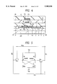
- FIG. 1 is a plan view of a memory cell in an SRAM embodying the invention
- FIG. 2 is a cross-sectional view taken on line A-A' in FIG. 1;
- FIG. 3 is a cross-sectional view taken on line B-B' in FIG. 1;
- FIG. 4 is a cross-sectional view taken on line B'-B" in FIG. 1;
- FIG. 5 is an equivalent circuit diagram of a memory cell in the SRAM
- FIG. 6 is a plan view showing a layout pattern comprising active regions, gate electrodes of driver MISFETs, and gate electrodes (word lines) of transfer MISFETs constituting a memory cell;
- FIG. 7 is a plan view depicting a layout pattern including active regions, gate electrodes of driver MISFETs, and gate electrodes (word lines) of transfer MISFETs constituting four memory cells;
- FIG. 8 is a schematic plan view of a semiconductor substrate, showing one phase of the process for fabricating a memory cell of the SRAM embodying the invention
- FIG. 9 is a cross-sectional view taken on line A-A' in FIG. 8;
- FIG. 10 is a cross-sectional view taken on line B-B' in FIG. 8;
- FIG. 11 is a cross-sectional view taken on line B"-B' in FIG. 8;
- FIG. 12 is another schematic plan view of the semiconductor substrate, showing another phase of the process for fabricating a memory cell of the SRAM embodying the invention
- FIG. 13 is a cross-sectional view taken on line A-A' in FIG. 12;
- FIG. 14 is a cross-sectional view taken on line B-B' in FIG. 12;
- FIG. 15 is a cross-sectional view taken on line B"-B' in FIG. 12;
- FIG. 16 is a schematic cross-sectional view of the semiconductor substrate, depicting another phase of the process for fabricating a memory cell of the SRAM embodying the invention.
- FIG. 17 is another schematic cross-sectional view of the semiconductor substrate, depicting another phase of the process for fabricating a memory cell of the SRAM embodying the invention.
- FIG. 18 is another schematic cross-sectional view of the semiconductor substrate, depicting another phase of the process for fabricating a memory cell of the SRAM embodying the invention.
- FIGS. 19A and 19B are schematic plan views of the semiconductor substrate, illustrating other phases of the process for fabricating a memory cell of the SRAM embodying the in invention
- FIG. 20 is a cross-sectional view taken on line A-A' in FIG. 19A;
- FIG. 21 is a cross-sectional view taken on line B-B' in FIG. 19A;
- FIG. 22 is a cross-sectional view taken on line B"-B' in FIG. 19A;
- FIG. 23 is another schematic cross-sectional view of the semiconductor substrate, showing another phase of the process for fabricating a memory cell of the SRAM embodying the invention.
- FIG. 24 is another schematic cross-sectional view of the semiconductor substrate, showing another phase of the process for fabricating a memory cell of the SRAM embodying the invention.
- FIG. 25 is another schematic cross-sectional view of the semiconductor substrate, showing another phase of the process for fabricating a memory cell of the SRAM embodying the invention
- FIG. 26 is another schematic plan view of the semiconductor substrate, showing another phase of the process for fabricating a memory cell of the SRAM embodying the invention
- FIG. 27 is a cross-sectional view taken on line A-A' in FIG. 26;
- FIG. 28 is a cross-sectional view taken on line B-B' in FIG. 26;
- FIG. 29 is another schematic plan view of the semiconductor substrate, illustrating another phase of the process for fabricating a memory cell of the SRAM embodying the invention.
- FIG. 30 is a cross-sectional view taken on line A-A' in FIG. 29;
- FIG. 31 is a cross-sectional view taken on line B-B' in FIG. 29;
- FIG. 32 is another schematic plan view of the semiconductor substrate, illustrating another phase of the process for fabricating a memory cell of the SRAM embodying the invention
- FIG. 33 is a cross-sectional view taken on line A-A' in FIG. 32;
- FIG. 34 is a cross-sectional view taken on line B-B' in FIG. 32;
- FIG. 35 is another schematic plan view of the semiconductor substrate, illustrating another phase of the process for fabricating a memory cell of the SRAM embodying the invention
- FIG. 36 is a cross-sectional view taken on line A-A' in FIG. 35;
- FIG. 37 is a cross-sectional view taken on line B-B' in FIG. 35;
- FIG. 38 is another schematic plan view of the semiconductor substrate, illustrating another phase of the process for fabricating a memory cell of the SRAM embodying the invention.
- FIG. 39 is a cross-sectional view taken on line A-A' in FIG. 38;
- FIG. 40 a cross-sectional view taken on line B-B' in FIG. 38;
- FIG. 41 is a plan view showing schematically the gate capacitance memory cell
- FIG. 42 is a schematic cross-sectional view of a semiconductor substrate, illustrating a bipolar CMOS SRAM embodying the invention
- FIG. 43 is a schematic cross-sectional view of another semiconductor substrate, illustrating another bipolar CMOS SRAM embodying the invention.
- FIG. 44 is an overall plan view depicting an SRAM chip layout
- FIG. 45 is an equivalent circuit diagram of an SRAM memory cell
- FIG. 46 is a plan view portraying a layout pattern including active regions, gate electrodes of driver MISFETs, and gate electrodes (word lines) of transfer MISFETs constituting a memory cell;
- FIGS. 47A and 47B are plan views depicting schematically the gate capacitance of a memory cell
- FIG. 48 is a schematic plan view of a semiconductor substrate, illustrating one phase of the conventional process for fabricating an SRAM memory cell
- FIG. 49 is a cross-sectional view taken on line A-A' in FIG. 48;
- FIG. 50 is a cross-sectional view taken on line B-B' in FIG. 48;
- FIG. 51 is another schematic cross-sectional view of the semiconductor substrate, illustrating another phase of the conventional process for fabricating an SRAM memory cell
- FIG. 52 another schematic cross-sectional view of the semiconductor substrate, illustrating another phase of the conventional process for fabricating an SRAM memory cell
- FIG. 53 a schematic plan view of the semiconductor substrate, showing another phase of the conventional process for fabricating an SRAM memory cell
- FIG. 54 is a cross-sectional view taken on line A-A' in FIG. 53;
- FIG. 55 is a cross-sectional view taken on line B-B' in FIG. 53;
- FIG. 56 is another schematic plan view of the semiconductor substrate, showing another phase of the conventional process for fabricating an SRAM memory cell
- FIG. 57 is a cross-sectional view taken on line A-A' in FIG. 56;
- FIG. 58 is a cross-sectional view taken on line B-B' in FIG. 56;
- FIG. 59 is another schematic plan view of the semiconductor substrate, showing another phase of the conventional process for fabricating an SRAM memory cell
- FIG. 60 is a cross-sectional view taken on line A-A' in FIG. 59;
- FIG. 61 is a cross-sectional view taken on line B-B' in FIG. 59;
- FIG. 62 is another schematic plan view of the semiconductor substrate, showing another phase of the conventional process for fabricating an SRAM memory cell
- FIG. 63 is a cross-sectional view taken on line A-A' in FIG. 62;
- FIG. 64 is a cross-sectional view taken on line B-B' in FIG. 62;
- FIG. 65 is another schematic plan view of the semiconductor substrate, showing another phase of the conventional process for fabricating an SRAM memory cell
- FIG. 66 is a cross-sectional view taken on line A-A' in FIG. 65;
- FIG. 67 is a cross-sectional view taken on line B-B' in FIG. 65;
- FIG. 68 is a graphic representation of data indicating how dependent the amount of gate electrode edge shrink is on the mask size in the traverse direction, the shrink being attributed to an optical wraparound effect upon photo resist exposure;
- FIG. 69 is a graphic representation of typical relationships between the soft error rate and the operating voltage of SRAM memory cells.
- FIG. 1 is a plan view of a memory cell in an SRAM embodying the invention
- FIG. 2 is a cross-sectional view taken on line A-A' in FIG. 1
- FIG. 3 is a cross-sectional view taken on line B-B' in FIG. 1
- FIG. 4 is a cross-sectional view taken on line B'-B" in FIG. 1
- FIG. 5 is an equivalent circuit diagram of a memory cell in the SRAM.
- FIG. 1 illustrates only the conductive layers of the memory cell, and omits showing insulating films between the conductive layers as well as some other parts.
- a memory cell in the SRAM embodying the invention comprises a pair of driver MISFETs Qd 1 and Qd 2 , a pair of resistor elements R 1 and R 2 acting as load elements, a pair of transfer MISFETs Qt 1 and Qt 2 , a pair of complementary data lines (DL, bar DL), and a pair of word lines WL 1 and WL 2 .
- This memory cell has its load elements composed of, but not limited to, high resistance load type elements.
- the two driver MISFETs Qd 1 and Qd 2 and the pair of resistor elements R 1 and R 2 constitute a flip-flop circuit that acts as a data storage part for storing one-bit data.
- the source region of the transfer MISFET Qt 1 is connected to one of two input terminals of the flip-flop circuit (i.e., to storage node A); the source region of the transfer MISFET Qt 2 is connected to the other input terminal of the flip-flop circuit (i.e., to storage node B).
- the driver MISFETs Qd 1 and Qd 2 and the transfer MISFETs Qt 1 and Qt 2 are each an n-channel MISFET.
- the driver MISFETs Qd 1 and Qd 2 and the transfer MISFETs Qt 1 and Qt 2 are formed in active regions 4 surrounded by a field insulating film 3 formed on the main surface of a p-type well 2 in the semiconductor substrate 1 illustratively composed of p - type silicon single crystal.
- Gate electrodes 5 of the driver MISFETs Qd 1 and Qd 2 and gate electrodes 6 (word lines WL 1 and WL 2 ) of the transfer MISFETs Qt 1 and Qt 2 are each made of a first layer polycrystal silicon film formed above the main surface of the p-type well 2.
- a dose of n-type impurities e.g., phosphorus (P) are implanted into the polycrystal silicon film.
- the gate electrodes 5 of the driver MISFETs Qd 1 and Qd 2 and the gate electrodes 6 of the transfer MISFETs Qt 1 and Qt 2 are located mostly over the active regions with a gate insulating film 7 interposed therebetween.
- the gate insulating film 7 is made up of silicon oxide.
- the word line WL 1 formed integrally with the gate electrode 6 of the transfer MISFET Qt 1 and the word line WL 2 formed integrally with the gate electrode 6 of the transfer MISFET Qt 2 are located principally over the field insulating film 3.
- the word lines WL 1 and WL 2 extend perpendicularly to the direction in which the gate electrodes 5 of the driver MISFETs Qd 1 and Qd 2 extend.
- the gate electrodes 5 of the driver MISFETs Qd 1 and Qd 2 and the gate electrodes 6 (word lines WL 1 and WL 2 ) of the transfer MISFETs Qt 1 and Qt 2 ) may be constituted alternatively by a polycide film having a high-melting-point metal silicide film (WSi x (tungsten silicide), MoSi x (molybdenum silicide), TiSi x (titanium silicide), etc.) deposited over the polycrystal silicon film.
- WSi x tungsten silicide
- MoSi x molybdenum silicide
- TiSi x titanium silicide
- FIG. 6 is a plan view showing a layout pattern comprising the active regions 4, the gate electrodes 5 of the driver MISFETs Qd 1 and Qd 2 , and the gate electrodes 6 (word lines WL 1 and WL 2 ) of the transfer MISFETs Qt 1 and Qt 2 constituting a memory cell.
- the driver MISFETs Qd 1 and Qd 2 , transfer MISFETs Qt 1 and Qt 2 , storage nodes A and B, and word lines WL 1 and WL 2 correspond to their counterpart circuits in FIG. 5.
- the SRAM embodying the invention is fabricated under design rules on fabrication conforming to a scaled-down design of 0.4 ⁇ m but not limited thereto.
- the line width Lw of the word lines WL 1 and WL 2 on the field insulating film 3 is 0.4 ⁇ m
- the gate length Lt of the gate electrodes 6 for the transfer MISFETs Qt 1 and Qt 2 is 0.85 ⁇ m
- the gate length Ld of the gate electrodes 5 in a channel forming region for the driver MISFETs Qd 1 and Qd 2 is 1.0 ⁇ m.
- the gate length of MISFETs constituting peripheral circuits, not shown, is 0.4 ⁇ m.
- the gate length Ld of the driver MISFETs Qd 1 and Qd 2 in the channel forming region, and the gate length Le of the driver MISFETs Qd 1 and Qd 2 near the edge of the active regions 4, are both at least double the minimum gate length of the MISFETs constituting memory cells or peripheral circuits.
- the line width of the word lines for the memory cells and the minimum gate length of the MISFETs constituting the peripheral circuits are designed in accordance with the minimum resolution increment of the demagnifying projection aligner in use.
- the minimum resolution increment is adopted as the word line width and as the MISFET gate length
- the amount of shrink on the word lines and gate electrodes is increased in the longitudinal direction upon optical exposure.
- the amount of shrink ( ⁇ z) on the word lines (gate electrodes) becomes 0.3 ⁇ m or more, as shown in FIG. 68.
- the gate length (Le, Ld) of the gate electrodes 5 for the driver MISFETs Qd 1 and Qd 2 is made at least double the minimum resolution increment (0.4 ⁇ m) of the demagnifying projection aligner as in the case of the above embodiment the amount of shrink ( ⁇ z) on the edge of the gate electrodes 5 becomes practically negligible.
- the reduction in the mask alignment allowance (x) may be matched with an enlarged area of the active regions 4, thus permitting an effective increase in the gate width for the driver MISFETs Qd 1 and Qd 2 . This allows the gate capacitance (Cox) to be raised without increasing the memory cell size.
- the gate length Le of the driver MISFETs Qd 1 and Qd 2 near the edge of the active regions 4 is made longer (e.g., to about 1.5 ⁇ m) than the gate length Ld (1.0 ⁇ m) in the channel forming region.
- This arrangement additionally enlarges the area of the gate electrodes 5 for the driver MISFETs Qd 1 and Qd 2 , whereby the gate capacitance (Cox) is enhanced further.
- the source and drain regions of the transfer MISFET Qt 1 are made of an n - type semiconductor region 8 of low impurity density and an n + type semiconductor region 9 of high impurity density.
- the source and drain regions of the transfer MISFET Qt 2 are also made of the n - type semiconductor region 8 of low impurity density and the n + type semiconductor region 9 of high impurity density. That is, the transfer MISFETs Qt 1 and Qt 2 have a lightly doped drain (LDD) structure.
- LDD lightly doped drain
- the driver MISFET Qd 1 has the same LDD structure as the transfer MISFETs Qt 1 and Qt 2 .
- the drain region of the driver MISFET Qd 1 is composed of the n + type semiconductor region 9 of high impurity density and an n-type semiconductor region 10 overlapping considerably with the gate electrodes 5.
- the drain region of the driver MISFET Qd 2 is composed of the n + type semiconductor region 9 of high impurity density and the n-type semiconductor region 10 overlapping considerably with the gate electrodes 5.
- the overlapping length of the drain regions for the driver MISFETs Qd 1 and Qd 2 is made at least double the overlapping length between the gate electrode and the drain region (or source region) of the MISFET having the minimum gate length in any peripheral circuit of the cell, not shown.
- the n-type semiconductor region 10 (drain region) of the driver MISFETs Qd 1 and Qd 2 is made to overlap considerably with the gate electrodes 5. This arrangement compensates for that drop in driver capability which is attributable to the prolonged gate length of the driver MISFETs Qd 1 and Qd 2 . Thus it is possible to raise the gate capacity (Cox) without lowering the driving capability of the driver MISFETs Qd 1 and Qd 2 .
- the source region of the driver MISFET Qd 1 is made of the n - type semiconductor region 8 of low impurity density and the n + type semiconductor region 9 of high impurity density. But as shown in FIG. 4, this source region is not located near the edge of the active regions (encircled "OFF" location in FIG. 4). Although not shown in FIG. 4, the source region of the driver MISFET Qd 2 is similarly not located near the edge of the active regions. This means that the source regions of the driver MISFETs Qd 1 and Qd 2 are offset near the edge of the active regions with respect to the gate electrodes 5 (i.e., offset structure).
- the source and drain regions of the driver MISFETs Qd 1 and Qd 2 is offset against the gate electrodes 5 near the edge of the active regions 4.
- the drain and source regions of the driver MISFETs Qd 1 and Qd 2 do not come close to each other at the edge of the active regions 4 even when the mask alignment allowance (x) is reduced so as to let the edge of the gate electrodes 5 on the field insulating film 3 approach the active regions 4.
- the mask alignment allowance (x) is reduced so as to let the edge of the gate electrodes 5 on the field insulating film 3 approach the active regions 4.
- no leaks occur between the storage nodes (i.e., drain region) and the reference voltage (i.e., source region).
- the above structure allows the area of the active regions 4 to be enlarged without increasing the memory cell size and without destabilizing the data being held in the cell. This, in turn makes it possible to enlarge the area of the gate electrodes 5 for the driver MISFETs Qd 1 and Qd 2 , thereby raising the gate capacitance (Cox).
- the above structure may be replaced by one of two other offset structures.
- One offset structure involves offsetting the drain region side of the driver MISFETs Qd 1 and Qd 2 near the edge of the active regions.
- the other alternative offset structure involves offsetting both the source and the drain region near the edge of the active regions. In any case, the effects obtained are the same.
- FIG. 7 is a plan view depicting a layout pattern including the active regions 4, the gate electrodes 5 of the driver MISFETs Qd 1 and Qd 2 , and the gate electrodes 6 (word lines WL 1 and WL 2 ) of the transfer MISFETs Qt 1 and Qt 2 constituting four memory cells.
- a spacing distance (or gap) (a) between the gate electrode 5 of the driver MISFET Qd 1 and the gate electrode 6 (word line WL 1 ) of the transfer MISFET Qt 1 is made the same (0.4 ⁇ m) in at least two directions; a spacing distance (or gap) (b) between the gate electrode 5 of the driver MISFET Qd 1 in this cell and that of a driver MISFET Qd 1 in an adjacent memory cell in a row (or word line) direction is made the same as the spacing distance (a) above (0.4 ⁇ m).
- the spacing distance between the gate electrode 5 of the driver MISFET Qd 2 and the gate electrode 6 (word line WL 2 ) of the transfer MISFET Qt 2 is also made the same (0.4 ⁇ m) in at least two directions; the spacing distance between the gate electrode 5 of the driver MISFET Qd 2 in this cell and that of the driver MISFET Qd 2 in the adjacent memory cell in the word line direction is made the same as the above space (0.4 ⁇ m).
- a structure as that just described results in the following benefit: the structure prevents excess exposure light from sneaking to the edge of the gate electrodes 5 when a photo resist pattern is formed.
- the pattern is used by the demagnifying projection aligner exposing the photo resist film to fabricate the gate electrodes 5 of the driver MISFETs Qd 1 and Qd 2 and the gate electrodes 6 (word lines WL 1 and WL 2 ) of the transfer MISFETs Qt 1 and Qt 2 . This prevents the contraction of the photo resist pattern at the edge portion of the gate electrodes 5. With the contraction of the photo resist pattern forestalled, the mask alignment allowance (x) for the edge portion of the gate electrodes 5 is reduced.
- the reduction in the mask alignment allowance (x) is matched with an enlarged area of the active regions 4, whereby the gate width for the driver MISFETs Qd 1 and Qd 2 is effectively increased. This in turn allows the gate capacitance (Cox) to be raised without increasing the memory cell size.
- each memory cell in the SRAM embodying of the invention has three kinds of space distances kept identical (0.4 ⁇ m): a spacing distance (a) between the gate electrode 5 of the driver MISFET Qd 1 and the gate electrode 6 (word line WL 1 ) of the transfer MISFET Qt 1 ; a line width (c) of the word line WL 1 ; and a spacimg distance (d) between the word line WL 1 and the word line WL 1 in the adjacent memory cell in a perpendicular, column direction.
- spacing distances are also held identical (0.4 ⁇ m) in each memory cell: the spacing distance between the gate electrode 5 of the driver MISFET Qd 2 and the gate electrode 6 (word line WL 2 ) of the transfer MISFET Qt 2 ; the line width of the word line WL 2 ; and the spacing distance between the word line WL 2 and the word line WL 2 in the adjacent memory cell in the column direction.
- the above structure affords pattern periodicity to three kinds of space: the space (a) between the gate electrodes 5 on the one hand and the gate electrodes 6 on the other (word line WL 1 , WL 2 ); the line width (c) of the word lines WL 1 and WL 2 ; and the space (d) between the word lines WL 1 and WL 2 , on the one hand, and the word lines WL 1 and WL 2 on the other in the adjacent memory cell, near the edge of the gate electrodes 5 for the driver MISFETs Qd 1 and Qd 2 .
- the photo resist pattern is formed for use by the demagnifying projection aligner exposing the photo resist film to fabricate the gate electrodes 5 of the driver MISFETs Qd 1 and Qd 2 and the gate electrodes 6 (word lines WL 1 and WL 2 ) of the transfer MISFETs Qd 1 and Qd 2 , it is possible to prevent the contraction of the photo resist pattern at the edge of the gate electrodes 5.
- the mask alignment allowance (x) for the edge portion of the gate electrodes 5 is reduced.
- the reduction in the mask alignment allowance (x) is matched with an enlarged area of the active regions 4, whereby the gate width for the driver MISFETs Qd 1 and Qd 2 is effectively increased. This in turn allows the gate capacitance (Cox) to be raised without increasing the memory cell size.
- wiring 12A of low resistance, pad layers 12B and 12C, and resistor elements R 1 and R 2 are deposited over the gate electrodes 5 of the driver MISFETs Qd 1 and Qd 2 and over the gate electrodes 6 (word lines WL 1 and WL 2 ) of the transfer MISFETs Qd 1 and Qd 2 , the electrodes being covered with a silicon oxide film 11.
- the wiring 12A, pad layers 12B and 12C, and resistor elements R 1 and R 2 are constituted by the second layer polycrystal silicon film.
- a dose of n-type impurities e.g., phosphorus (P)
- P phosphorus
- each of the resistor elements R 1 and R 2 is supplied with a circuit power source voltage (Vcc) via the wiring 12A.
- the other end of each of the resistor elements R 1 and R 2 is connected via connecting holes 15 both to the drain region (n + type semiconductor region 9) on one side of the driver MISFETs Qd 1 and Qd 2 , and to the gate electrodes 5 on the other side thereof.
- the high resistance load type memory cell is made smaller than ever by locating the resistor elements R 1 and R 2 in the layer above the driver MISFETs Qd 1 and Qd 2 .
- Wiring 17A, a pad layer 17B and word shunts 17C are deposited over a silicon oxide layer insulating film 16 that covers the wiring 12A, pad layers 12B and 12C, and resistor elements R 1 and R 2 .
- the wiring 17A, pad layer 17B and word shunts 17C are composed of the first layer aluminum film.
- the wiring 17A is connected to the source regions (n + type semiconductor region 9) of the driver MISFETs Qd 1 and Qd 2 via the pad layer 12C and connecting holes 14 and 19.
- the source regions are connected to the circuit reference voltage Vss via the wiring 17A.
- the word shunts 17C are connected to the word lines WL 1 and WL 2 via connecting holes formed in regions not shown over the layer insulating film 16.
- Data lines (DL, bar DL) are formed over a second layer insulating film 20 that covers the wiring 17A, pad layer 17B and word shunts 17C.
- the data lines (DL, bar DL) are made up of the second layer aluminum film.
- One data line (DL) is connected to the drain region (n + type semiconductor region 9) of the transfer MISFET Qt 1 via connecting holes 22 in the layer insulating film 20, the pad layer 17B, connecting holes 18 in the layer insulating film 16, the pad layer 12B, and connecting holes 13.
- the other data line (bar DL) is connected to the drain region (n + type semiconductor region 9) of the transfer MISFET Qt 2 via the connecting holes 22, pad layer 17B, connecting holes 18, pad layer 12B, and connecting holes 13.
- a final passivation film 21 is formed over the data lines (DL, bar DL), i.e., on top of the semiconductor substrate 1, the film 21 being made of a silicon oxide film or of a layered film comprising a silicon oxide film and a silicon nitride film.
- FIGS. 8 through 40 the plan views show only the conductive layers of the memory cell and not the layer insulating films therebetween.
- FIG. 9 cross-sectional view taken on line A-A' in FIG. 8
- FIG. 10 cross-sectional view taken on line B-B' in FIG. 8
- FIG. 11 cross-sectional view taken on line B"-B' in FIG. 8
- a p-type well 2 and a field insulating film 3 are first formed on the main surface of a p-type semiconductor substrate 1.
- a gate insulating film 7 is then formed over the surface of active regions 4 surrounded by the field insulating film 3.
- the first layer polycrystal silicon film deposited by CVD (chemical vapor deposition) method on the semiconductor substrate 1 is patterned into gate electrodes 5 of the driver MISFETs Qd 1 and Qd 2 and gate electrodes 6 (word lines WL 1 and WL 2 ) of the transfer MISFETs Qt 1 and Qt 2 over the gate insulating film 7.
- the patterning proceeds specifically as follows: a photo resist film is formed over the first layer polycrystal silicon film. The photo resist film is then exposed and developed to produce a photo resist pattern R. With the photo resist pattern R used as the mask, the polycrystal silicon film is removed selectively by dry etching using illustratively CF 4 gas or the like. The etching forms the gate electrodes 5 and 6.
- n-type impurity ions e.g., phosphorus (P)
- P phosphorus
- the field insulating film 3, photo resist film 23, gate electrodes 5 and gate electrodes 6 are used as the mask.
- the semiconductor substrate 1 is annealed so as to expand and diffuse the implanted impurities sufficiently. This produces an n-type semiconductor region 10 overlapping considerably with the gate electrodes 5, as shown in FIGS. 16, 17 and 18.
- the n-type semiconductor region 10 constitutes the drain edge portion of the drain regions for the driver MISFETs.
- the photo resist film 23 is formed so as to cover the regions constituting the source regions of the driver MISFETs Qd 1 and Qd 2 and the source and drain regions of the transfer MISFETs Qt 1 and Qt 2 .
- the implantation of impurities to form the n-type semiconductor region 10 is carried out in such a manner that the drain edge portion of the driver MISFETs is defined by the gate electrodes 5 and by the field insulating film 3 in the gate width direction (i.e., Y direction) of the driver MISFETS, but not by the photo resist film 23. As shown in FIG.
- the X direction is the direction in which the word lines WL 1 and WL 2 extend. Furthermore, the X direction is in parallel with the gate length direction of the driver MISFETs. The Y direction is perpendicular to the X direction, and is parallel to the gate width direction of the driver MISFETS.
- FIG. 19A cross-sectional view taken on line A-A' in FIG. 19A
- FIG. 21 cross-sectional view taken on line B-B' in FIG. 19A
- FIG. 22 cross-sectional view taken on line B"-B' in FIG. 19A.
- n-type impurity ions e.g., phosphorus
- n-type impurity ions e.g., phosphorus
- the n - type semiconductor region 8 is not formed near the edge portion of the active regions covered with the photo resist film 24, as depicted in FIG. 22. That is, as shown in FIG.
- the implantation of impurities to form the n - type semiconductor region is directed only to the shaded portions in the active regions 4, and not to the regions 4".
- the source regions of the driver MISFETs Qd 1 and Qd 2 are offset against the gate electrodes 5 near the edge of the active regions.
- the offset structure gets the photo resist film 24 to cover the active regions 4" and the gate electrodes 5 at the edge of the active regions 4 even when edges of the gate electrodes 5 shrink on the active regions 4 as a result of mask misalignment or edge contraction of the gate electrodes 5. That is, no impurities are implanted to the regions 4" while the n-type semiconductor region is being formed. This prevents the drain and source regions of the driver MISFETs Qd 1 and Qd 2 from coming close to one another at the edge of the active regions 4. With the drain and source regions set apart, no leak current or conductance occurs therebetween. This makes it possible to reduce the mask alignment allowance and to lessen the memory cell size accordingly.
- the silicon oxide film deposited by CVD method on the semiconductor substrate 1 is etched anisotropically into side wall spacers 26 of the side walls for both the gate electrodes 5 of the driver MISFETs Qd 1 and Qd 2 and the gate electrodes 6 (word lines WL 1 and WL 2 ) of the transfer MISFETs Qt 1 and Qt 2 .
- the side wall spacers 26 thus formed, the p-type well 2 near the edge of the active regions constituting the source regions of the driver MISFETs Qd 1 and Qd 2 is covered with a photo resist film 25, as shown in FIGS. 23, 24 and 25.
- n-type impurity ions e.g., arsenic (As)
- As arsenic
- a silicon oxide film 11 is deposited by CVD method over the gate electrodes 5 and gate electrodes 6 (word lines WL 1 and WL 2 ) to form connecting holes, as depicted in FIG. 26, FIG. 27 (cross-sectional view taken on line A-A' in FIG. 26) and FIG. 28 (cross-sectional view taken on line B-B' in FIG. 26).
- the connecting holes thus formed comprise connecting holes 13 and 14 reaching the n + type semiconductor region 9, and connecting holes 15 spanning the n + type semiconductor region 9 and the gate electrodes 5 of the driver MISFETs Qd 1 and Qd 2 .
- a second layer polycrystal silicon film 12 is deposited by CVD method on the silicon oxide film 11. The polycrystal silicon film 12 is patterned into the plan layout shown in FIG. 26.
- a photo resist film 27 is used as the mask with which n-type impurity ions (e.g., phosphorus, arsenic, antimony (Sb)) are implanted into part of the polycrystal silicon film 12.
- n-type impurity ions e.g., phosphorus, arsenic, antimony (Sb)
- the ion implantation forms the wiring 12A of low resistance, pad layers 12B and 12C, and resistor elements R 1 and R 2 , as depicted in FIG. 32, FIG. 33 (cross-sectional view taken on line A-A' in FIG. 32) and FIG. 34 (cross-sectional view taken on line B-B' in FIG. 32).
- the silicon oxide layer insulating film 16 is deposited by CVD method over the wiring 12A, pad layers 12B and 12C, and resistor elements R 1 and R 2 to form connecting holes, as depicted in FIG. 35, FIG. 36 (cross-sectional view taken on line A-A' in FIG. 35) and FIG. 37 (cross-sectional view taken on line B-B' in FIG. 35).
- the connecting holes thus formed comprise connecting holes 18 reaching the pad layer 12B, and connecting holes 19 reaching the pad layer 12C.
- a first layer aluminum film is deposited by sputtering onto the layer insulating film 16, and is patterned into the wiring 17A, pad layer 17B, and word shunts 17C. For the ease of viewing, FIG.
- FIG. 38 FIG. 39 (cross-sectional view taken on line A-A' in FIG. 38) and FIG. 40 (cross-sectional view taken on line B-B' in FIG. 38)
- a silicon oxide layer insulating film 20 is deposited by CVD method over the wiring 17A, pad layer 17B and word shunts 17C to form connecting holes 22 reaching the pad layer 17B.
- a second layer aluminum film is deposited by sputtering over the layer insulating film 20, and is patterned into the data lines (DL, bar DL). For the ease of viewing, FIG.
- the final passivation film 21 is deposited by CVD method over the data lines (DL, bar DL). This completes the fabrication of the high resistance load type memory cell shown in FIGS. 1 through 4 and embodying the invention.
- FIG. 41 is a plan view showing schematically the gate capacitance (Cox) of a memory cell embodying the invention, the gate capacitance being in effect when the storage node A is at the high potential level.
- the gate capacitance (Cox 2 ) of the driver MISFET Qd 2 being turned on comprises two components: one formed in a channel forming region (indicated by hatching pattern), the other in a capacitance-dedicated region (indicated by shadow pattern).
- the gate capacitance (Cox 1 ) of the driver MISFET Qd 1 being turned off is generated in the overlapping area between the gate and the drain electrode (indicated by hatching pattern).
- the gate capacitance (Cox) component is raised to 11.3 fF from 2.1 fF for the memory cell shown in FIG. 47A. This increases the total storage node capacitance from 5.8 fF to 15 fF. As a result, as shown in FIG. 69, it becomes possible for the memory cells of the invention to attain the soft error rate of 50 Fit or less even when the power supply voltage (Vcc) is lowered from 5.0 ⁇ 0.3 V to 3.3 ⁇ 0.3 V.
- FIG. 42 is a schematic cross-sectional view of a semiconductor substrate, illustrating a bipolar CMOS SRAM embodying the invention.
- This bipolar CMOS SRAM combines memory cells of the invention with peripheral circuits composed of n-channel MISFETs Qn of the LDD structure, p-channel MISFETs Qp, and npn bipolar transistors Qb.
- Each n-channel MISFET Qn of the peripheral circuits is formed on the main surface of the p-type well 2 formed over a p-type buried layer 80 of high impurity density.
- the n-channel MISFET Qn is constituted by source and drain regions which comprise a gate insulating film 81, gate electrodes 82 made of the first layer polycrystal silicon film, an n - type semiconductor region 83 of low impurity density, and an n + type semiconductor region 84 of high impurity density.
- the source and drain regions are connected to wiring 17D via a pad layer 12D composed of the second layer polycrystal silicon film.
- the wiring 17D is made of the first layer aluminum film.
- Each p-channel MISFET Qp is formed over the main surface of an n-type well 86 furnished on an n + type buried layer 85 of high impurity density.
- the p-channel MISFET Qp is constituted by source and drain regions which comprise the gate insulating film 81, the gate electrodes 87 made of the first layer polycrystal silicon film, a p - type semiconductor region 88 of low impurity density, and a p + type semiconductor region 89 of high impurity density.
- the source and drain regions are connected to wiring 96 via a pad layer 17E composed of the first layer aluminum film.
- the wiring 96 is made of the second layer aluminum film.
- Each npn bipolar transistor Qb uses the n+ type buried layer 85 of high impurity density as a buried collector, on which is formed an n-type well that acts as an intrinsic collector.
- the npn bipolar transistor Qb is constituted by the n + type buried layer 85, the n-type well 86, a collector forming region 90 made of an n-type semiconductor region, an intrinsic base region 91, an external base region 92 formed simultaneously with the p + type semiconductor region 89 of the p-channel MISFET Qp, an emitter extraction electrode 93 made of the second layer polycrystal silicon film, and an emitter region 94 produced by thermally diffusing n-type impurities from the emitter extraction electrode 93 to part of the intrinsic base region 91.
- the external base region 92, emitter extraction electrode 93 and collector forming region 90 are connected respectively with the wiring portions 17F, 17G and 17H made of the first layer aluminum film.
- Each memory cell is formed on the main surface of the p-type well 2 furnished over a p-type buried layer 80. To prevent destruction of data caused by noise from peripheral circuits, the entire memory cell array bottom is surrounded by an n-type buried layer 95, and the memory cell array sides are surrounded by the n+ type buried layer 85.
- the drain regions (i.e., n-type semiconductor region 10 overlapping significantly with the gate electrodes 5) of the driver MISFETs Qd 1 and Qd 2 in a memory cell are in contact with the p-type buried layer 80 at the cell bottom.
- This arrangement increases the pn junction component (Cpn) of the storage node capacitance, so that the resistance to soft errors is further enhanced.
- the memory cells instead of being formed as high resistance load type memory cells in one embodiment described above, may be composed of complete CMOS memory cells comprising load p-channel MISFETs of a TFT (thin film transistor) structure deposited over the driver MISFETS.
- FIG. 43 is a schematic cross-sectional view of a semiconductor substrate, illustrating a bipolar CMOS SRAM combining complete CMOS memory cells with peripheral circuits which include n-channel MISFETs Qn of the LDD structure, p-channel MISFETs Qp and npn bipolar transistors Qb.
- the load MISFET Qp 1 is constituted by a gate electrode 100 made of the second layer polycrystal silicon film, by a p-type source region 101s made of the third layer polycrystal silicon film deposited on the gate electrode 100 with a silicon oxide gate insulating film 102 interposed therebetween, by a p-type drain region 101d, and by a nondoped channel region 101c.
- the drain region 101d of the load MISFET Qp 1 is connected to the gate electrode 100 of another load MISFET Qp 2 , not shown, and is further connected via the gate electrode 100 to the drain region (n + type semiconductor region 9) of the transfer MISFET Qt 2 .
- the structure of the other parts in the memory cell and that of the associated peripheral circuits are the same as those of the bipolar CMOS SRAM shown in FIG. 42.
- the present invention may also be applied to an SRAM having memory cells whose loads are constituted by bulk p-channel MISFETs formed on a semiconductor substrate.
- the memory cells may also be combined with a stacked capacitor structure involving three or more polycrystal silicon film layers. The arrangement if implemented increases the capacitance of storage nodes, whereby the operating voltage required is further reduced.
- the invention may be applied to a CMOS SRAM or a bipolar CMOS SRAM with its devices separated by U-grooves formed on the semiconductor substrate.
- the invention may also be applied to a CMOS SRAM or a bipolar CMOS SRAM whose devices are formed on an SOI substrate having an insulating layer (e.g., silicon oxide layer) interposed between a semiconductor substrate and a buried layer.
- an insulating layer e.g., silicon oxide layer
- At least one of the source and drain regions of the driver MISFET is offset against the gate electrode. This prevents leaks from occurring between the storage node (drain region) and the reference voltage (source region) even when the mask alignment allowance for the gate electrode edge is reduced to let the edge of the gate electrode on the field insulating film approach the active regions.
- the mask alignment allowance for the gate electrode edge is reduced, it is possible to enlarge the area of the active regions without increasing the memory cell size and to enhance the effective area of the gate electrode of the driver MISFETs, whereby the gate capacitance component of the storage node capacitance is boosted.
- the spacing distance (or gap) between the gate electrode of the driver MISFET and that of the transfer MISFET is made substantially the same in at least two directions.
- the spacing distance (or gap) between the gate electrode of the driver MISFET in this cell and that of a driver MISFET in an adjacent memory cell is made substantially equal to the spacing distance (or gap) between the gate electrode of the driver MISFET and that of the transfer MISFET.
- the mask alignment allowance for the gate electrode edge is reduced, it is possible to enlarge the area of the active regions without increasing the memory cell size and to enhance the effective area of the gate electrode of the driver MISFETs, whereby the gate capacitance component of the storage node capacitance is boosted.
- the spacing distance (or gap) between the gate electrode of the driver MISFET and that of the transfer MISFET, the line width of the gate electrode of the transfer MISFET, and the spacing distance (or gap) between the gate electrode of the transfer MISFET and that of the transfer MISFET in the adjacent memory cell are all made substantially the same.
- This arrangement affords periodicity to three kinds of spacing distances: the spacing distance (or gap) between the gate electrode of the driver MISFET and the gate electrode (word line) of the transfer MISFET, the line width of the word line, and the spacing distance (or gap) between adjacently disposed word lines, near the edge of the gate electrodes for the driver MISFETs.
- the photo resist pattern is formed for use by the demagnifying projection aligner exposing the photo resist film to fabricate the gate electrodes of the driver MISFETs and the gate electrodes (word lines) of the transfer MISFETs, it is possible to prevent the contraction of the photo resist pattern at the edge of the gate electrodes of the driver MISFETs.
- the mask alignment allowance for the edge portion of the gate electrode is reduced.
- the area of the active regions is increased without enlarging the memory cell size, and the effective area of the gate electrodes for the driver MISFETs is boosted so as to raise the gate capacitance component of the storage node capacitance.
- the gate length of the intrinsic channel forming region of the driver MISFET is made at least double the gate length of the MISFET which has the shortest gate length and which constitutes part of a memory cell or a peripheral circuit. This arrangement makes substantially negligible the amount of contraction of the gate electrode edge during gate electrode fabrication.
- the mask alignment allowance for the edge portion of the gate electrode is reduced. It follows that the area of the active regions is increased without enlarging the memory cell size, and that the effective area of the gate electrodes for the driver MISFETs is boosted so as to raise the gate capacitance component of the storage node capacitance.
- the overlapping length between the gate electrode and the drain region of the driver MISFET is made at least double the overlapping length between the gate electrode and the drain region of the MISFET having the minimum gate length in any memory cell or peripheral circuit. This arrangement prevents the driving capability from dropping when the gate length of the driver MISFET is prolonged.
- the gate length of the driver MISFET near the active regions is made longer than the gate length in the channel forming region. This makes it possible to enlarge the area of the gate electrodes of the driver MISFETs and to boost the gate capacitance component of the storage node capacitance.
- a semiconductor region which has a conductivity type different from that of the drain region and which has a higher level of impurity density than the semiconductor substrate.
- the semiconductor region is located so as to contact the drain region bottom. This arrangement increases the pn junction component of the storage node capacity.
Landscapes
- Engineering & Computer Science (AREA)
- Physics & Mathematics (AREA)
- Condensed Matter Physics & Semiconductors (AREA)
- General Physics & Mathematics (AREA)
- Manufacturing & Machinery (AREA)
- Computer Hardware Design (AREA)
- Microelectronics & Electronic Packaging (AREA)
- Power Engineering (AREA)
- Semiconductor Memories (AREA)
Priority Applications (1)
| Application Number | Priority Date | Filing Date | Title |
|---|---|---|---|
| US08/820,247 US5903036A (en) | 1993-11-22 | 1997-03-18 | Semiconductor device having MISFET SRAM cells in which active regions and gate electrodes are dimensioned for increasing storage node capacitances without increasing memory cell size |
Applications Claiming Priority (4)
| Application Number | Priority Date | Filing Date | Title |
|---|---|---|---|
| JP5-291948 | 1993-11-22 | ||
| JP5291948A JPH07142608A (ja) | 1993-11-22 | 1993-11-22 | 半導体集積回路装置 |
| US34399494A | 1994-11-18 | 1994-11-18 | |
| US08/820,247 US5903036A (en) | 1993-11-22 | 1997-03-18 | Semiconductor device having MISFET SRAM cells in which active regions and gate electrodes are dimensioned for increasing storage node capacitances without increasing memory cell size |
Related Parent Applications (1)
| Application Number | Title | Priority Date | Filing Date |
|---|---|---|---|
| US34399494A Continuation | 1993-11-22 | 1994-11-18 |
Publications (1)
| Publication Number | Publication Date |
|---|---|
| US5903036A true US5903036A (en) | 1999-05-11 |
Family
ID=17775537
Family Applications (1)
| Application Number | Title | Priority Date | Filing Date |
|---|---|---|---|
| US08/820,247 Expired - Lifetime US5903036A (en) | 1993-11-22 | 1997-03-18 | Semiconductor device having MISFET SRAM cells in which active regions and gate electrodes are dimensioned for increasing storage node capacitances without increasing memory cell size |
Country Status (3)
| Country | Link |
|---|---|
| US (1) | US5903036A (ja) |
| JP (1) | JPH07142608A (ja) |
| KR (1) | KR950015793A (ja) |
Cited By (6)
| Publication number | Priority date | Publication date | Assignee | Title |
|---|---|---|---|---|
| US6212671B1 (en) * | 1997-10-20 | 2001-04-03 | Mitsubishi Electric System Lsi Design Corporation | Mask pattern data producing apparatus, mask pattern data producing method and semiconductor integrated circuit device |
| US6359319B1 (en) * | 1997-04-25 | 2002-03-19 | Nec Corporation | Static random access memory cell having pocket regions adjacent to sources of drive transistors |
| US20020085409A1 (en) * | 2000-12-29 | 2002-07-04 | Houston Theodore W. | Static random access memory cell and method |
| FR2849962A1 (fr) * | 2003-01-13 | 2004-07-16 | St Microelectronics Sa | Condensateur enterre associe a une cellule sram |
| US20070141766A1 (en) * | 2005-12-15 | 2007-06-21 | Shinsaku Sekido | Semiconductor circuit device and design method therefor |
| CN110729288A (zh) * | 2018-07-16 | 2020-01-24 | 台湾积体电路制造股份有限公司 | 静态随机存取存储器外围电路的布局 |
Families Citing this family (3)
| Publication number | Priority date | Publication date | Assignee | Title |
|---|---|---|---|---|
| KR100265763B1 (ko) * | 1997-12-31 | 2000-09-15 | 윤종용 | 스태틱 랜덤 억세스 메모리 장치 및 그 제조방법 |
| JP4142228B2 (ja) * | 2000-02-01 | 2008-09-03 | 株式会社ルネサステクノロジ | 半導体集積回路装置 |
| JP5068296B2 (ja) * | 2009-09-25 | 2012-11-07 | ルネサスエレクトロニクス株式会社 | 半導体記憶装置の製造方法 |
Citations (2)
| Publication number | Priority date | Publication date | Assignee | Title |
|---|---|---|---|---|
| US5239196A (en) * | 1990-02-09 | 1993-08-24 | Shuji Ikeda | SRAM with dual word lines overlapping drive transistor gates |
| US5461251A (en) * | 1993-07-28 | 1995-10-24 | United Microelectronics Corporation | Symmetric SRAM cell with buried N+ local interconnection line |
-
1993
- 1993-11-22 JP JP5291948A patent/JPH07142608A/ja active Pending
-
1994
- 1994-11-11 KR KR1019940029586A patent/KR950015793A/ko not_active Application Discontinuation
-
1997
- 1997-03-18 US US08/820,247 patent/US5903036A/en not_active Expired - Lifetime
Patent Citations (2)
| Publication number | Priority date | Publication date | Assignee | Title |
|---|---|---|---|---|
| US5239196A (en) * | 1990-02-09 | 1993-08-24 | Shuji Ikeda | SRAM with dual word lines overlapping drive transistor gates |
| US5461251A (en) * | 1993-07-28 | 1995-10-24 | United Microelectronics Corporation | Symmetric SRAM cell with buried N+ local interconnection line |
Cited By (15)
| Publication number | Priority date | Publication date | Assignee | Title |
|---|---|---|---|---|
| US6359319B1 (en) * | 1997-04-25 | 2002-03-19 | Nec Corporation | Static random access memory cell having pocket regions adjacent to sources of drive transistors |
| US6212671B1 (en) * | 1997-10-20 | 2001-04-03 | Mitsubishi Electric System Lsi Design Corporation | Mask pattern data producing apparatus, mask pattern data producing method and semiconductor integrated circuit device |
| US20020085409A1 (en) * | 2000-12-29 | 2002-07-04 | Houston Theodore W. | Static random access memory cell and method |
| US6687145B2 (en) * | 2000-12-29 | 2004-02-03 | Texas Instruments Incorporated | Static random access memory cell and method |
| WO2004066350A3 (fr) * | 2003-01-13 | 2004-11-11 | St Microelectronics Sa | Condensateur enterre associe a une cellule sram |
| WO2004066350A2 (fr) * | 2003-01-13 | 2004-08-05 | Stmicroelectronics Sa | Condensateur enterre associe a une cellule sram |
| FR2849962A1 (fr) * | 2003-01-13 | 2004-07-16 | St Microelectronics Sa | Condensateur enterre associe a une cellule sram |
| US20060232909A1 (en) * | 2003-01-13 | 2006-10-19 | Jean-Pierre Schoellkopf | Embedded capacitor associated with an sram cell |
| US7638828B2 (en) | 2003-01-13 | 2009-12-29 | Stmicroelectronics S.A. | Embedded capacitor |
| US20070141766A1 (en) * | 2005-12-15 | 2007-06-21 | Shinsaku Sekido | Semiconductor circuit device and design method therefor |
| US7562327B2 (en) * | 2005-12-15 | 2009-07-14 | Panasonic Corporation | Mask layout design improvement in gate width direction |
| CN110729288A (zh) * | 2018-07-16 | 2020-01-24 | 台湾积体电路制造股份有限公司 | 静态随机存取存储器外围电路的布局 |
| CN110729288B (zh) * | 2018-07-16 | 2022-01-04 | 台湾积体电路制造股份有限公司 | 静态随机存取存储器外围电路的布局 |
| US11342340B2 (en) | 2018-07-16 | 2022-05-24 | Taiwan Semiconductor Manufacturing Co., Ltd. | Layout of static random access memory periphery circuit |
| US11856747B2 (en) | 2018-07-16 | 2023-12-26 | Taiwan Semiconductor Manufacturing Company, Ltd. | Layout of static random access memory periphery circuit |
Also Published As
| Publication number | Publication date |
|---|---|
| KR950015793A (ko) | 1995-06-17 |
| JPH07142608A (ja) | 1995-06-02 |
Similar Documents
| Publication | Publication Date | Title |
|---|---|---|
| US6303425B1 (en) | Semiconductor device and method of manufacturing the same | |
| US5317178A (en) | Offset dual gate thin film field effect transistor | |
| US6737712B2 (en) | Method of manufacturing semiconductor integrated circuit device having capacitor element | |
| US6531363B2 (en) | Method for manufacturing a semiconductor integrated circuit of triple well structure | |
| US4890148A (en) | Semiconductor memory cell device with thick insulative layer | |
| US20110260253A1 (en) | Semiconductor device | |
| US4849801A (en) | Semiconductor memory device having increased capacitance for the storing nodes of the memory cells | |
| JP2601176B2 (ja) | 半導体記憶装置 | |
| US6228704B1 (en) | Process for manufacturing semiconductor integrated circuit device | |
| JPH04162668A (ja) | 半導体装置およびその製造方法 | |
| US6204538B1 (en) | SRAM cell | |
| US5903036A (en) | Semiconductor device having MISFET SRAM cells in which active regions and gate electrodes are dimensioned for increasing storage node capacitances without increasing memory cell size | |
| US5592011A (en) | Single layer thin film transistor static random access memory cell | |
| US4780751A (en) | Semiconductor integrated circuit device | |
| US5331170A (en) | Static type random access memory device with stacked memory cell free from parasitic diode | |
| KR19980071712A (ko) | 전원배선에 평형한 데이터선을 가진 스태틱 반도체 메모리 | |
| JP2689923B2 (ja) | 半導体装置およびその製造方法 | |
| US5917247A (en) | Static type memory cell structure with parasitic capacitor | |
| US6440790B1 (en) | Method of making semiconductor device having an insulating film positioned between two similarly shaped conductive films | |
| US4967257A (en) | Semiconductor device having field effect transistors | |
| JP2702999B2 (ja) | 半導体記憶装置 | |
| US20060102965A1 (en) | Semiconductor device | |
| JP2877069B2 (ja) | スタティック型半導体メモリ装置 | |
| JPH01166554A (ja) | 半導体記憶装置 | |
| JPH0279468A (ja) | 半導体記憶装置およびその製造方法 |
Legal Events
| Date | Code | Title | Description |
|---|---|---|---|
| AS | Assignment |
Owner name: HITACHI, LTD., JAPAN Free format text: ASSIGNMENT OF ASSIGNORS INTEREST;ASSIGNOR:ONOZAWA, KAZUNORI;REEL/FRAME:009542/0477 Effective date: 19940927 |
|
| STCF | Information on status: patent grant |
Free format text: PATENTED CASE |
|
| FEPP | Fee payment procedure |
Free format text: PAYOR NUMBER ASSIGNED (ORIGINAL EVENT CODE: ASPN); ENTITY STATUS OF PATENT OWNER: LARGE ENTITY |
|
| FPAY | Fee payment |
Year of fee payment: 4 |
|
| FEPP | Fee payment procedure |
Free format text: PAYOR NUMBER ASSIGNED (ORIGINAL EVENT CODE: ASPN); ENTITY STATUS OF PATENT OWNER: LARGE ENTITY Free format text: PAYER NUMBER DE-ASSIGNED (ORIGINAL EVENT CODE: RMPN); ENTITY STATUS OF PATENT OWNER: LARGE ENTITY |
|
| FPAY | Fee payment |
Year of fee payment: 8 |
|
| FPAY | Fee payment |
Year of fee payment: 12 |
|
| AS | Assignment |
Owner name: RENESAS ELECTRONICS CORPORATION, JAPAN Free format text: ASSIGNMENT OF ASSIGNORS INTEREST;ASSIGNOR:HITACHI, LTD.;REEL/FRAME:026109/0528 Effective date: 20110307 |