US5672906A - Semiconductor device having defects of deep level generated by electron beam irradiation in a semiconductor substrate - Google Patents
Semiconductor device having defects of deep level generated by electron beam irradiation in a semiconductor substrate Download PDFInfo
- Publication number
- US5672906A US5672906A US08/588,395 US58839596A US5672906A US 5672906 A US5672906 A US 5672906A US 58839596 A US58839596 A US 58839596A US 5672906 A US5672906 A US 5672906A
- Authority
- US
- United States
- Prior art keywords
- semiconductor
- integrated circuit
- semiconductor device
- type
- circuit device
- Prior art date
- Legal status (The legal status is an assumption and is not a legal conclusion. Google has not performed a legal analysis and makes no representation as to the accuracy of the status listed.)
- Expired - Lifetime
Links
- 239000004065 semiconductor Substances 0.000 title claims abstract description 131
- 230000007547 defect Effects 0.000 title claims description 8
- 238000010894 electron beam technology Methods 0.000 title abstract description 31
- 239000000758 substrate Substances 0.000 title abstract description 30
- XUIMIQQOPSSXEZ-UHFFFAOYSA-N Silicon Chemical compound [Si] XUIMIQQOPSSXEZ-UHFFFAOYSA-N 0.000 claims abstract description 24
- 229910052710 silicon Inorganic materials 0.000 claims abstract description 24
- 239000010703 silicon Substances 0.000 claims abstract description 24
- 230000004913 activation Effects 0.000 claims abstract description 15
- 230000005669 field effect Effects 0.000 claims description 5
- 239000013078 crystal Substances 0.000 claims description 4
- 230000000295 complement effect Effects 0.000 claims 1
- 238000000034 method Methods 0.000 abstract description 28
- 238000000137 annealing Methods 0.000 abstract description 19
- 239000012535 impurity Substances 0.000 abstract description 17
- 238000004519 manufacturing process Methods 0.000 abstract description 15
- 239000000969 carrier Substances 0.000 abstract description 10
- 230000005516 deep trap Effects 0.000 abstract description 8
- 230000006798 recombination Effects 0.000 abstract description 8
- 238000005215 recombination Methods 0.000 abstract description 6
- 206010047571 Visual impairment Diseases 0.000 abstract description 2
- 230000008569 process Effects 0.000 description 14
- 230000001678 irradiating effect Effects 0.000 description 10
- 102100031920 Dihydrolipoyllysine-residue succinyltransferase component of 2-oxoglutarate dehydrogenase complex, mitochondrial Human genes 0.000 description 7
- 101000992065 Homo sapiens Dihydrolipoyllysine-residue succinyltransferase component of 2-oxoglutarate dehydrogenase complex, mitochondrial Proteins 0.000 description 7
- 238000001773 deep-level transient spectroscopy Methods 0.000 description 7
- 230000004907 flux Effects 0.000 description 7
- 238000010586 diagram Methods 0.000 description 6
- 238000002161 passivation Methods 0.000 description 5
- 238000005520 cutting process Methods 0.000 description 3
- QVGXLLKOCUKJST-UHFFFAOYSA-N atomic oxygen Chemical compound [O] QVGXLLKOCUKJST-UHFFFAOYSA-N 0.000 description 2
- 230000005540 biological transmission Effects 0.000 description 2
- 230000008859 change Effects 0.000 description 2
- 230000007423 decrease Effects 0.000 description 2
- 230000000694 effects Effects 0.000 description 2
- 239000010931 gold Substances 0.000 description 2
- 229910001385 heavy metal Inorganic materials 0.000 description 2
- 238000002368 isothermal capactiance transient spectroscopy Methods 0.000 description 2
- 238000005259 measurement Methods 0.000 description 2
- 229910052760 oxygen Inorganic materials 0.000 description 2
- 239000001301 oxygen Substances 0.000 description 2
- 238000011084 recovery Methods 0.000 description 2
- 238000000926 separation method Methods 0.000 description 2
- 238000012360 testing method Methods 0.000 description 2
- 208000032368 Device malfunction Diseases 0.000 description 1
- 239000004698 Polyethylene Substances 0.000 description 1
- 230000009471 action Effects 0.000 description 1
- 230000003321 amplification Effects 0.000 description 1
- 238000010168 coupling process Methods 0.000 description 1
- 238000005859 coupling reaction Methods 0.000 description 1
- 230000000994 depressogenic effect Effects 0.000 description 1
- 230000006866 deterioration Effects 0.000 description 1
- 238000009792 diffusion process Methods 0.000 description 1
- PCHJSUWPFVWCPO-UHFFFAOYSA-N gold Chemical compound [Au] PCHJSUWPFVWCPO-UHFFFAOYSA-N 0.000 description 1
- 229910052737 gold Inorganic materials 0.000 description 1
- 238000010438 heat treatment Methods 0.000 description 1
- 239000002784 hot electron Substances 0.000 description 1
- 230000006872 improvement Effects 0.000 description 1
- 238000002347 injection Methods 0.000 description 1
- 239000007924 injection Substances 0.000 description 1
- 230000003993 interaction Effects 0.000 description 1
- 239000012299 nitrogen atmosphere Substances 0.000 description 1
- 238000003199 nucleic acid amplification method Methods 0.000 description 1
- 230000003071 parasitic effect Effects 0.000 description 1
- -1 polyethylene Polymers 0.000 description 1
- 229920000573 polyethylene Polymers 0.000 description 1
- 230000000630 rising effect Effects 0.000 description 1
Images


Classifications
-
- H—ELECTRICITY
- H01—ELECTRIC ELEMENTS
- H01L—SEMICONDUCTOR DEVICES NOT COVERED BY CLASS H10
- H01L27/00—Devices consisting of a plurality of semiconductor or other solid-state components formed in or on a common substrate
- H01L27/02—Devices consisting of a plurality of semiconductor or other solid-state components formed in or on a common substrate including semiconductor components specially adapted for rectifying, oscillating, amplifying or switching and having at least one potential-jump barrier or surface barrier; including integrated passive circuit elements with at least one potential-jump barrier or surface barrier
- H01L27/04—Devices consisting of a plurality of semiconductor or other solid-state components formed in or on a common substrate including semiconductor components specially adapted for rectifying, oscillating, amplifying or switching and having at least one potential-jump barrier or surface barrier; including integrated passive circuit elements with at least one potential-jump barrier or surface barrier the substrate being a semiconductor body
- H01L27/08—Devices consisting of a plurality of semiconductor or other solid-state components formed in or on a common substrate including semiconductor components specially adapted for rectifying, oscillating, amplifying or switching and having at least one potential-jump barrier or surface barrier; including integrated passive circuit elements with at least one potential-jump barrier or surface barrier the substrate being a semiconductor body including only semiconductor components of a single kind
-
- H—ELECTRICITY
- H01—ELECTRIC ELEMENTS
- H01L—SEMICONDUCTOR DEVICES NOT COVERED BY CLASS H10
- H01L29/00—Semiconductor devices adapted for rectifying, amplifying, oscillating or switching, or capacitors or resistors with at least one potential-jump barrier or surface barrier, e.g. PN junction depletion layer or carrier concentration layer; Details of semiconductor bodies or of electrodes thereof ; Multistep manufacturing processes therefor
- H01L29/02—Semiconductor bodies ; Multistep manufacturing processes therefor
- H01L29/30—Semiconductor bodies ; Multistep manufacturing processes therefor characterised by physical imperfections; having polished or roughened surface
- H01L29/32—Semiconductor bodies ; Multistep manufacturing processes therefor characterised by physical imperfections; having polished or roughened surface the imperfections being within the semiconductor body
-
- H—ELECTRICITY
- H01—ELECTRIC ELEMENTS
- H01L—SEMICONDUCTOR DEVICES NOT COVERED BY CLASS H10
- H01L27/00—Devices consisting of a plurality of semiconductor or other solid-state components formed in or on a common substrate
- H01L27/02—Devices consisting of a plurality of semiconductor or other solid-state components formed in or on a common substrate including semiconductor components specially adapted for rectifying, oscillating, amplifying or switching and having at least one potential-jump barrier or surface barrier; including integrated passive circuit elements with at least one potential-jump barrier or surface barrier
- H01L27/04—Devices consisting of a plurality of semiconductor or other solid-state components formed in or on a common substrate including semiconductor components specially adapted for rectifying, oscillating, amplifying or switching and having at least one potential-jump barrier or surface barrier; including integrated passive circuit elements with at least one potential-jump barrier or surface barrier the substrate being a semiconductor body
- H01L27/08—Devices consisting of a plurality of semiconductor or other solid-state components formed in or on a common substrate including semiconductor components specially adapted for rectifying, oscillating, amplifying or switching and having at least one potential-jump barrier or surface barrier; including integrated passive circuit elements with at least one potential-jump barrier or surface barrier the substrate being a semiconductor body including only semiconductor components of a single kind
- H01L27/085—Devices consisting of a plurality of semiconductor or other solid-state components formed in or on a common substrate including semiconductor components specially adapted for rectifying, oscillating, amplifying or switching and having at least one potential-jump barrier or surface barrier; including integrated passive circuit elements with at least one potential-jump barrier or surface barrier the substrate being a semiconductor body including only semiconductor components of a single kind including field-effect components only
- H01L27/088—Devices consisting of a plurality of semiconductor or other solid-state components formed in or on a common substrate including semiconductor components specially adapted for rectifying, oscillating, amplifying or switching and having at least one potential-jump barrier or surface barrier; including integrated passive circuit elements with at least one potential-jump barrier or surface barrier the substrate being a semiconductor body including only semiconductor components of a single kind including field-effect components only the components being field-effect transistors with insulated gate
- H01L27/092—Devices consisting of a plurality of semiconductor or other solid-state components formed in or on a common substrate including semiconductor components specially adapted for rectifying, oscillating, amplifying or switching and having at least one potential-jump barrier or surface barrier; including integrated passive circuit elements with at least one potential-jump barrier or surface barrier the substrate being a semiconductor body including only semiconductor components of a single kind including field-effect components only the components being field-effect transistors with insulated gate complementary MIS field-effect transistors
- H01L27/0921—Means for preventing a bipolar, e.g. thyristor, action between the different transistor regions, e.g. Latchup prevention
Definitions
- the present invention relates to a structure and a manufacturing method of a monocrystal silicon semiconductor substrate and a semiconductor device and a manufacturing method of it.
- the semiconductor device relates to a semiconductor integrated circuit device employing CMOS structure, a semiconductor image sensor device, and a semiconductor device having a bipolar element.
- FIG. 18 is a schematic cross section showing a conventional semiconductor integrated circuit device employing CMOS structure.
- This is a general CMOS-type semiconductor integrated circuit device having a N-type well 1015 of N-type impurity concentration about 3E16 atms/cm 3 which is provided on a P-type silicon semiconductor substrate 1016 of P-type impurity concentration about 7E14 atms/cm 3 . It constitutes a N-channel MOS transistor 1010 and a P-channel MOS transistor 1009.
- the P-channel MOS transistor 1009 constitutes equivalently a PNP bipolar transistor Tr1 1001.
- the N-channel MOS transistor 1010 constitutes equivalently a NPN bipolar transistor Tr2 1003.
- the PNP bipolar transistor 1001 the NPN bipolar transistor Tr2 1003 include an effective resistivity Rn 1002 and Rp 1004 respectively between a base and a emitter. Then they from an equivalent circuit as shown in FIG. 19.
- a surge current 1021 is sent to an input terminal 1020 to a certain amount, a carrier 1022 generated by the surge current diffuses.
- a collector current of the actuated transistor functions as a base current of the other transistor and so actuates the other transistor.
- the current is supplied continuously to the base of the transistor actuated earlier and so the current keeps on flowing between a power supply electrode Vcc 1005 and a power supply electrode Vss 1006 even after the surge current, which has been a first trigger, ceases. Then the semiconductor integrated circuit device malfunctions. Furthermore, in the worst case, its wiring pattern fuses. This phenomenon is called latch-up. Usually, a semiconductor integrated circuit device must not cause latch-up to the surge current and noises to some electrical value. This value is called latch-up resistance. Then the measures taken to raise the latch-up resistance are as followings: One of them is to lower the effective resistivity Rp 1004 and Rn 1002 shown in Figures.
- Means for lowering resistivity are to raise impurity concentration of the substrate 1016, to raise impurity concentration of the well 1015, and to use an epi wafer. (As shown in FIG.
- P + -type substrate 1023 of about 1E18-1E20 atms/cm 3 concentration as a semiconductor substrate and a P - -type layer of about several ⁇ m--several tens ⁇ m concentration which is performed epitaxial growth on the surface of the P + -type substrate and which corresponds to the P - -type semiconductor substrate 1016 in FIG. 18.
- a region 1012 is a P+-type diffusion region
- regions 1013, 1014, 1017, and 1018 are N + -type impurity regions.
- 1011 is a gate electrode of the MOS transistor.
- a first problem is as follows; When the substrate impurity concentration and the well impurity concentration are increased, channel conductance of a MOS transistor is declined and then necessary current value, that means, plane size of a transistor to get an action speed becomes large, so the chip size (plane size of a semiconductor integrated circuit device) is increased. That invites rising costs. Besides, VTH (threshold voltage) of a MOS transistor, that is acting voltage as a semiconductor integrated circuit device rises and the increase of both VTH and a leakage current cannot be prevented at the same time. The durability of a semiconductor device declines because of hot electrons. Therefore the increase of the concentrations is limited to some extent.
- a second problem is that enlarging the sizes L1 and L2 shown in FIG. 18 and providing a guard ring make the chip size larger.
- a third problem is that using an epi wafer highly rises the manufacturing cost of a semiconductor substrate.
- the cost will be about a few times to ten times as high as the cost of a substrate having no epi wafer.
- the object of the present invention is to provide a CMOS semiconductor device having large latch-up resistance.
- Another object of the present invention is to provide a semiconductor image sensor device which acquires high resolution when interaction of photoelectric carriers between sensors is hindered.
- Another object is to provide a semiconductor device having a bipolar transistor which is superior in switching characteristic.
- Another object is to provide a silicon semiconductor substrate for a semiconductor device containing controlled crystal defects (traps) of the shallow level and the deep level.
- Another object is to provide a manufacturing method with which the characteristics of a semiconductor device can be easily controlled after the semiconductor device is completed.
- the present invention employs the following means.
- a semiconductor substrate having the shallow level traps and the deep level traps which function as recombination centers in a band gap of silicon is obtained.
- the shallow level traps have the activation energy from a valence band EV of under 0.1 eV at 150 K. and their concentration is about 1.2-1.7 E15/cm 3 .
- the deep level traps have the activation energy of about 0.28-0.32 eV at 150 K. and their concentration is about 1.6-2.0 E13/cm 3 .
- the defects traps of deep level have the maximum value in DLTS signal at 150 K.
- a semiconductor substrate stated in 1 is manufactured in a method which includes a process of irradiating an electron beam of over 2 MeV at a density of over 1 E14/cm 2 .
- a semiconductor substrate stated in 1 is manufactured in a method which includes a process of irradiating an electron beam of over 2 MeV at a density of over 1 E14/cm 2 to only a specified part.
- a semiconductor substrate stated in 2 and 3 is manufactured in a method which includes a process of irradiating an electron beam in a container which is airtight and from which the air has been pumped out at a vacuum of over 1 E-2 Torr (high degree of vacuum).
- a semiconductor substrate stated in 2-4 is manufactured in a method which includes a process of annealing at over 200 ° C.
- a semiconductor device having the shallow level traps and the deep level traps which function as recombination centers in a band gap of silicon is obtained.
- the shallow level traps have the activation energy from a valence band EV of under 0.1 eV at about 150 K (kelvin temperature) and their concentration is about 1.2-1.7 E15/cm 3 .
- the deep level traps have the activation energy of about 0.28-0.32 eV at about 150 K. and their concentration is about 1.6-2.0 E13/cm 3 .
- a semiconductor device a part of which has the shallow levels and the deep levels functioning as recombination centers in a band gap of silicon is obtained.
- the shallow level traps have the activation energy from a valence band EV of under 0.1 eV at about 150 K. and their concentration is about 1.2-1.7 E15/cm 3 .
- the deep level traps have the activation energy of about 0.28-0.32 eV at about 150 K. and their concentration is about 1.6-2.0 E13/cm 3 .
- a semiconductor device stated in 6 and 7 is manufactured in a method which includes a process of irradiating an electron beam of over 2 MeV at a density of over 1 E14/cm 2 .
- a semiconductor device stated in 6 and 7 is manufactured in a method which includes a process of irradiating an electron beam of over 2 MeV at a density of over 1 E14/cm 2 to a specified part.
- a semiconductor device stated in 6 and 7 is manufactured in a method which includes a process of irradiating an electron beam in a container which is airtight and from which the air has been pumped out at a vacuum of over 1 E-2 Torr (high degree of a vacuum).
- a semiconductor device stated in 6 and 7 is manufactured in a method which includes a process of annealing at over 200 ° C.
- a semiconductor device stated in 6 and 7 which employs CMOS structure comprising a P-type insulating gate field effect transistor and a N-type insulating gate field effect transistor.
- a semiconductor device stated in 6 and 7 which is a semiconductor image sensor device wherein a plurality of photo sensors are provided at regular intervals on a semiconductor region is obtained.
- a semiconductor device stated in 6 and 7 which includes a bipolar element comprising an emitter region and a collector region of reverse conducting type and contiguous to a base region having crystal defects of deep level is obtained.
- a semiconductor device stated in 6 and 7 which employs BiCMOS structure comprising a CMOS circuit and a bipolar transistor.
- a manufacturing method of a semiconductor device stated in 8-11 which employs CMOS structure is used.
- the manufacturing method of a semiconductor device comprises the following process steps of; forming a pn-type junction by introducing an impurity of a second conducting type to a semiconductor region of a first conducting type, providing electric electrodes to each of the P-type semiconductor region and the N-type semiconductor region, forming a passivation film for protecting a semiconductor device from the outside, and irradiating an electron beam.
- a manufacturing method of a semiconductor device stated 8-11 which is a semiconductor image sensor device is employed.
- a manufacturing method of a semiconductor device stated in 8-11 and including a bipolar element is employed.
- a manufacturing method of a semiconductor device stated in 8-11 and employing BiCMOS structure is used.
- the level traps are formed suitably in a silicon substrate.
- FIG. 1 is a schematic cross section showing a part of a semiconductor integrated circuit device which is a first embodiment of a semiconductor device disclosed in the present invention
- FIG. 2 is a schematic plan view showing another part of a semiconductor integrated circuit device which is a first embodiment of a semiconductor device disclosed in the present invention
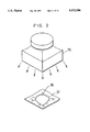
- FIG. 3 is a schematic view showing electron beam irradiation which is a manufacturing method of a semiconductor integrated circuit device which is a first embodiment of a semiconductor device disclosed in the present invention
- FIG. 4 is a schematic block diagram showing a circuit which is a general measuring method of latch-up resistance of a semiconductor integrated circuit device
- FIG. 5 is a graph showing a relation between IL after irradiation (As Exposed) and the quantity of irradiation;
- FIG. 6 is a graph showing a change of IL at irradiation and annealing
- FIG. 7 is a graph showing a relation between IL after annealing and the quantity of irradiation
- FIG. 8 is a graph showing a relation between tRR (recovery time of pn-type junction when electric current of 4 mA/mm 2 is sent at the forward direction) and the quantity of irradiation;
- FIG. 9 is a graph showing a relation of each irradiation beam between a leakage current of pn-type junction after annealing and tRR (minority-carrier lifetime);
- FIG. 10 is a graph showing a relation between a likeable current after annealing and IL
- FIG. 11 is a schematic plan view showing a semiconductor integrated circuit device which is a second embodiment of a semiconductor device disclosed in the present invention.
- FIG. 12 is a schematic blockdiagram showing a circuit of a semiconductor image sensor device
- FIG. 13 is a schematic view showing a section of A-A' in FIG. 12;
- FIG. 14 is a schematic view showing a section of B-B' in FIG. 12;
- FIG. 15 is a schematic cross section showing a semiconductor device which is a third embodiment of a semiconductor device disclosed in the present invention.
- FIG. 16 is a graph showing a relation between WB and Tstg
- FIG. 17 is a schematic cross section showing a part of a semiconductor integrated circuit device which is a fourth embodiment of a semiconductor device disclosed in the present invention.
- FIG. 18 is a schematic cross section showing a semiconductor integrated circuit device employing conventional CMOS structure
- FIG. 19 is a schematic block diagram showing an equivalent circuit of a semiconductor integrated circuit device employing conventional CMOS structure.
- FIG. 1 is a schematic cross section showing a part of a semiconductor integrated circuit device which is a first embodiment of a semiconductor device disclosed in the present invention. Its outward is similar to a conventional semiconductor device shown in FIG. 18. It is a schematic drawing and so an intermediate insulating layer, Al wiring, a surface protecting film (a passivation film) and so on are omitted.
- a CMOS circuit 23 comprises a N-channel MOS transistor 22 and a P-channel MOS transistor 24. 26 is a N-type well. 25 and 29 are P + -type impurity regions. 13, 16, 18, and 20 are N + -type impurity regions. 21 and 27 are gate electrodes of the MOS transistor.
- FIG. 2 is a schematic plan view showing a part of a semiconductor integrated circuit device which is a first embodiment of a semiconductor device disclosed in the present invention.
- a semiconductor device applied to this embodiment is 256 K bit SRAM employing CMOS-type circuit structure of about 4.4 ⁇ 13.0 mm in area (chip size). Its design rule is 1.0 ⁇ m rule.
- a substrate 11 is of P - -type and 20-30 ⁇ .cm in concentration.
- an epi wafer is applied to the substrate 11.
- an epi wafer is not used, even the shortest distance from an input terminal 12 to the CMOS portion 23 with a guard ring 15 in between in 300 ⁇ m and the latch-up resistance is only several dozens mA.
- the requirements for a semiconductor integrated circuit device are that the least latch-up resistance by current injection method is 100 mA and that Vcc is 5.5 V.
- an electron beam is irradiated to the semiconductor integrated circuit device which is perfection as an wafer finished passivation.
- FIG. 3 is a schematic diagram showing irradiation of an electron beam which is a manufacturing method of a semiconductor integrated circuit device which is the first embodiment of a semiconductor device disclosed in the present invention.
- a wafer 36 is put in a polyethylene bag 37. Air in this bag is pumped out so as to be vacuum at high degree of vacuum over 1E-2 Torr. Furthermore this bag is airtight The wafer is placed about one meter away from an irradiation nozzle 35 and an electron beam from a high energy electron beam generator is irradiated to the wafer in the air.
- FIG. 4 is a schematic block diagram showing a circuit which is a general way to measure latch-up resistance.
- a semiconductor integrated circuit device to be measured (D.U.T, which is short for Device Under Test) in injected 5.5 V to its Vcc and then current is injected to each of input terminals.
- the current value at which the semiconductor integrated circuit device starts latch-up is latch-up resistance (IL).
- FIG. 5 is a graph showing a relation between IL after irradiation and the quantity of irradiation.
- "Initial" means latch-up resistance before irradiation. It is observed that IL remarkably improves by irradiating an electron beam and a neutron flux. Irradiating r-rays improves IL very slightly. However, after irradiation, the semiconductor integrated circuit device (SRAM) does't work normally at all. That's because the value of a leakage current in pn-type junction and the value of VTH in a MOS transistor get excessively big.
- SRAM semiconductor integrated circuit device
- annealing heat treatment in N2 atmosphere
- the wafer irradiated an electron beam restores the characteristics of leakage current in pn-type junction and that of a MOS transistor enough.
- IL declines a little, however it is not a trouble.
- Annealing also restores the characteristics of leakage current in pn-type junction and that of a MOS transistor in the wafer irradiated a neutron flux, however, it is insufficient.
- FIG. 6 is a graph showing the change of the value of IL caused by irradiation and annealing.
- FIG. 7 is a graph showing a relation between IL after annealing and the quantity of irradiation. As seem from FIG. 7, the wafer irradiated an electron beam of over 2 MeV and over 1 E15/cm 2 only obtains necessary IL, and furthermore restores normal function of a semiconductor integrated circuit device.
- FIG. 8 is a graph showing a relation between tRR (recovery time of pn-type junction to which current of 4 mA/mm2 is sent at the forward direction) and the quantity of irradiation.
- tRR shows directly minority carrier lifetime and it follows that improvement of IL in the present invention is brought by the decline of minority carrier lifetime.
- the wafer irradiated a neutron flux does not restore enough the function of a semiconductor integrated circuit device, though it has IL of the same value as that of the wafer irradiated an electron beam. That is to say, mainly, there are much leakage current in pn-type junction.
- FIG. 9 is a graph showing a relation of each irradiation beam between a leakage current of pn-type junction after annealing and tRR (minority-carrier lifetime). It shows that a relation between a leakage current and a minority-carrier lifetime differs with beams. That means a position (level) of a recombination center formed in a band gap of silicon is different. Then a level of DLTS method D.V. Lang, Appl. Phys. 45-7 (1974), 3014, 3023.! and that of ICTS method H.Okushi and Y. Tokumura, Jpn. J. Appl. Phys. 19 (1980) L335.! are compared in a fixed quantity. Table 1 is a table showing measurement results of levels.
- a defect level produced by electron beam irradiation indicates the maximum value of a DLTS signal at 150 K.
- Its activation energy from valence band Ev; ⁇ E is under 0.1 eV.
- This deep level is about 1.6-2.0 E13/cm 3 in concentration and is in a band gap of silicon. Furthermore this deep level functions as a recombination center and then helps to improve latch-up resistance.
- the shallow levels of which the activation energy is under 0.1 eV are at a concentration of 1.2-1.7 E15/cm 3 .
- FIG. 10 is a graph showing a relation between a leakage current and IL after annealing.
- the distance from an input terminal to a CMOS portion of a semiconductor integrated circuit device employing CMOS structure is about 300 ⁇ m.
- the above-stated level is required for a semiconductor integrated circuit device which has a sufficient latch-up resistance without using an epi wafer, and furthermore of which a leakage current of pn-type junction is within the permissible level.
- a novel and excellent point of this present invention is here; Actually, trade-off between latch-up resistance, a leakage current, and other characteristics is not gained until the level in a silicon band gap is within the above-stated level. Therefore the above-stated level is formed (and the characteristics of a MOS transistor is also restored) by irradiating an electron beam of which the energy is over 2 MeV at a density of 1 e15/cm 2 and then annealing at 200°-300° C. for about one hour. This is very important. That's because the level can be formed by electron beam irradiation after a passivation process of the process sequence (a wafer process) of a semiconductor integrated circuit device as explained above.
- An electron beam can be irradiated after passivation film is formed as annealing is performed at a low temperature (200°-300° C.). Namely, if it is found that latch-up resistance is not enough because of an unexpected design mistake such as a size mistake at a testing process after a semiconductor integrated circuit device is completed, levels can be formed at that time. Of course, the levels can be provided in a wafer process, if so, the degree of freedom to provide conditions of annealing increases as a wafer can be heated over 500° C.
- the levels disclosed in the present invention can be provided or formed by electron beam irradiation. After a monocrystal silicon as semiconductor substrate is formed, the levels are formed by electron beam irradiation. Then a semiconductor device is formed with a manufacturing process of a semiconductor integrated circuit device. Electron beam irradiation can be done either before or after cutting in wafer-shape.
- an electron beam is irradiated to all the wafer.
- the process time is shortened, the increase of a leakage current of pn-type junction is suppressed, and the deterioration of the characteristics of a MOS transistor is lessened. This is hidden from the view, however obviously useful.
- FIG. 11 is a schematic plan view showing a semiconductor integrated circuit device which is a second embodiment of a semiconductor device disclosed in the present invention. It is a semiconductor image sensor device, which is a semiconductor integrated circuit device for receiving a light, converting the light into an electric signal, and outputting the electric signal. Now, this embodiment is explained with an example of a semiconductor image sensor device of line-type used in a facsimile and so on. In this device, several photo transistors are placed side by side and the sensor output is controlled by a control circuit portion 123 and is outputted from a pad 124.
- FIG. 12 is a schematic block diagram showing a circuit of a semiconductor image sensor device.
- photo transistors 121-122 which are NPN transistors of a floating base receive a light 129, generate an electric charge, and store the electric charge.
- the photo transistor When the photo transistor is selected by transmission gates 126 and 130, it outputs a collector current which is hFE times the electric charge stored by photo transistor to an output terminal 128.
- a reset transistor 125 is provided in order to initialize the output of the photo transistor as a sensor.
- a transmission gate B 127 is provided so as to forward the output to the output terminal 128.
- a pitch to arrange photo transistors of 64 bit is 125 ⁇ m in a semiconductor image sensor device of 8 dot/mm.
- FIG. 13 is a schematic diagram showing a section of A-A' shown in FIG. 11.
- FIG. 13 shows photo transistors placed side by side with each other.
- a photo transistor 141 comprises a emitter electrode 143, a N + -type emitter region 145, P - -type base region 144 and a N 31 -type collector region 146.
- Photoelectric carriers 147 occurred inside of the N - substrate 146 diffuse and scatter. Some photoelectric carriers are detected at the adjacent photo transistor 141, that means, signal separation between photo transistors (bits) is incompetent or the contrast is bad.
- bits signal separation between photo transistors
- the present invention without using an epi wafer, carriers diffusing to adjacent bits declines and good signal separation and good contrast is obtained. Some carriers remain even after the bit is selected and then cause the decline of the afterimage characteristic. However, the present invention can solve this problem well.
- FIG. 14 is a schematic view showing a section B-B' of FIG. 11. It shows a part of a semiconductor image sensor device which is adjacent to a chip edge 152.
- the chip edge 152 is a cross section cut with a dicing saw and the like.
- a region of N + -type layer 153 is prepared as a cutting portion which is referred to as a scribe area 154.
- a wafer is inspected in order to make sure of the quality.
- the semiconductor image sensor device detects signals by receiving the light, however, occasionally wrong signals appears from the bits located the edges of the sensors (the photo transistors 121-122). That's because the photoelectric carriers 151 generated by a light which entered the scribe area 154 diffuse and scatters.
- the present invention without an epi wafer, prevents the carriers generated by a light which entered the scribe area from getting into the sensors.
- This embodiment is described with a line-type semiconductor image sensor device, but the present invention can be also applied to a capacity-coupling type semiconductor image sensor device, so-called CCD (charge-coupled device).
- CCD charge-coupled device
- FIG. 15 is a schematic cross section showing a semiconductor device which is a third embodiment of the present invention. It is a signal NPN bipolar transistor comprising a emitter electrode 161, a base electrode 162, a N + -type emitter region 163, a P - -type base region 164, a P - -type guard ring region 168, a N + -type channel stopper region 169, a N - -type collector region 165, and a N + -type collector region 166.
- T off specifically the time that excessive minor carriers in the base region 164 is stored, Tstg.
- FIG. 16 is a graph showing a relation between WB and Tstg.
- Tstg of the inventive transistor irradiated an electron beam reduces by half in comparison with that of a transistor which is not irradiated any beam.
- FIG. 17 is a schematic cross section showing a part of a semiconductor integrated circuit device which is a fourth embodiment of a semiconductor device disclosed in the present invention. It is a BiCMOS-type semiconductor integrated circuit device in which the bipolar elements and the CMOS elements are intermingled. As described above, by applying the present invention, both good latch-up resistance in a CMOS portion 190 and good switching speed in a bipolar portion 183 can be obtained.
- the NPN bipolar portion 183 comprises a N + -type emitter region 185, a P - -type base region 182, and N + -type collector regions 184, 186, and 187, wherein each of the regions has an electrode.
- the CMOS portion 190 comprises a P-channel MOS transistor provided on the surface of a N - -type region 195 and a N-channel MOS transistor provided on the surface of a P - -type region 196.
- the P-channel transistor includes a P + -type impurity region 189 functioning as a source/drain region and a gate electrode 192.
- the N-channel MOS transistor includes a N + -type impurity region 193 functioning as a source/drain region and a gate electrode 194.
- an electron beam of over 2 MeV and 1 E15/cm 2 is irradiated to a wafer and then annealing is performed at over 200° C. to the wafer for more than one hour.
- shallow level traps of which the activation energy from valence band EV is under 0.1 eV and which are produced at a concentration of about 1.2-1.7 E15/cm 3 and deep level traps of which the activation energy is about 0.28-0.32 eV and which are provided at a concentration of about 1.6-2.0 E13/cm 3 are obtained.
Landscapes
- Engineering & Computer Science (AREA)
- Power Engineering (AREA)
- Microelectronics & Electronic Packaging (AREA)
- Physics & Mathematics (AREA)
- Condensed Matter Physics & Semiconductors (AREA)
- General Physics & Mathematics (AREA)
- Computer Hardware Design (AREA)
- Ceramic Engineering (AREA)
- Testing Or Measuring Of Semiconductors Or The Like (AREA)
- Semiconductor Integrated Circuits (AREA)
- Metal-Oxide And Bipolar Metal-Oxide Semiconductor Integrated Circuits (AREA)
Priority Applications (1)
| Application Number | Priority Date | Filing Date | Title |
|---|---|---|---|
| US08/588,395 US5672906A (en) | 1992-06-25 | 1996-01-18 | Semiconductor device having defects of deep level generated by electron beam irradiation in a semiconductor substrate |
Applications Claiming Priority (4)
| Application Number | Priority Date | Filing Date | Title |
|---|---|---|---|
| JP4-167076 | 1992-06-25 | ||
| JP16707692 | 1992-06-25 | ||
| US8196993A | 1993-06-24 | 1993-06-24 | |
| US08/588,395 US5672906A (en) | 1992-06-25 | 1996-01-18 | Semiconductor device having defects of deep level generated by electron beam irradiation in a semiconductor substrate |
Related Parent Applications (1)
| Application Number | Title | Priority Date | Filing Date |
|---|---|---|---|
| US8196993A Division | 1992-06-25 | 1993-06-24 |
Publications (1)
| Publication Number | Publication Date |
|---|---|
| US5672906A true US5672906A (en) | 1997-09-30 |
Family
ID=26491232
Family Applications (1)
| Application Number | Title | Priority Date | Filing Date |
|---|---|---|---|
| US08/588,395 Expired - Lifetime US5672906A (en) | 1992-06-25 | 1996-01-18 | Semiconductor device having defects of deep level generated by electron beam irradiation in a semiconductor substrate |
Country Status (2)
| Country | Link |
|---|---|
| US (1) | US5672906A (ko) |
| KR (1) | KR940006262A (ko) |
Cited By (6)
| Publication number | Priority date | Publication date | Assignee | Title |
|---|---|---|---|---|
| US5994162A (en) * | 1998-02-05 | 1999-11-30 | International Business Machines Corporation | Integrated circuit-compatible photo detector device and fabrication process |
| US6570198B2 (en) * | 2000-10-20 | 2003-05-27 | Seiko Instruments Inc. | Linear image sensor integrated circuit |
| US20040014254A1 (en) * | 1998-09-18 | 2004-01-22 | Capella Microsystems,Inc. | Photodetector and device employing the photodetector for converting an optical signal into an electrical signal |
| US20090206366A1 (en) * | 2008-02-15 | 2009-08-20 | Kazuyuki Sawada | Semiconductor device and method for fabricating the same |
| CN107112370A (zh) * | 2015-06-30 | 2017-08-29 | 富士电机株式会社 | 半导体装置及其制造方法 |
| CN113668064A (zh) * | 2021-07-29 | 2021-11-19 | 山西烁科晶体有限公司 | 一种优化碳化硅晶片电阻率的辐照方法 |
-
1993
- 1993-06-25 KR KR1019930011754A patent/KR940006262A/ko not_active Application Discontinuation
-
1996
- 1996-01-18 US US08/588,395 patent/US5672906A/en not_active Expired - Lifetime
Cited By (11)
| Publication number | Priority date | Publication date | Assignee | Title |
|---|---|---|---|---|
| US5994162A (en) * | 1998-02-05 | 1999-11-30 | International Business Machines Corporation | Integrated circuit-compatible photo detector device and fabrication process |
| US20040014254A1 (en) * | 1998-09-18 | 2004-01-22 | Capella Microsystems,Inc. | Photodetector and device employing the photodetector for converting an optical signal into an electrical signal |
| US6887735B2 (en) * | 1998-09-18 | 2005-05-03 | Capella Microsystems, Inc. | Photodetector and device employing the photodetector for converting an optical signal into an electrical signal |
| US6570198B2 (en) * | 2000-10-20 | 2003-05-27 | Seiko Instruments Inc. | Linear image sensor integrated circuit |
| US20090206366A1 (en) * | 2008-02-15 | 2009-08-20 | Kazuyuki Sawada | Semiconductor device and method for fabricating the same |
| US7759711B2 (en) * | 2008-02-15 | 2010-07-20 | Panasonic Corporation | Semiconductor device with substrate having increased resistance due to lattice defect and method for fabricating the same |
| CN107112370A (zh) * | 2015-06-30 | 2017-08-29 | 富士电机株式会社 | 半导体装置及其制造方法 |
| US20170301751A1 (en) * | 2015-06-30 | 2017-10-19 | Fuji Electric Co., Ltd. | Semiconductor device and method of manufacturing the same |
| US10134832B2 (en) * | 2015-06-30 | 2018-11-20 | Fuji Electric Co., Ltd. | Semiconductor device and method of manufacturing the same |
| CN107112370B (zh) * | 2015-06-30 | 2020-08-28 | 富士电机株式会社 | 半导体装置及其制造方法 |
| CN113668064A (zh) * | 2021-07-29 | 2021-11-19 | 山西烁科晶体有限公司 | 一种优化碳化硅晶片电阻率的辐照方法 |
Also Published As
| Publication number | Publication date |
|---|---|
| KR940006262A (ko) | 1994-03-23 |
Similar Documents
| Publication | Publication Date | Title |
|---|---|---|
| US4920396A (en) | CMOS having buried layer for carrier recombination | |
| US4484388A (en) | Method for manufacturing semiconductor Bi-CMOS device | |
| US4963973A (en) | Semiconductor device | |
| US4100561A (en) | Protective circuit for MOS devices | |
| US4047217A (en) | High-gain, high-voltage transistor for linear integrated circuits | |
| US20080142899A1 (en) | Radiation immunity of integrated circuits using backside die contact and electrically conductive layers | |
| JPS61154063A (ja) | 光半導体装置およびその製造方法 | |
| GB2090701A (en) | Improvements in or relating to input protection for MOS integrated circuits | |
| US3538399A (en) | Pn junction gated field effect transistor having buried layer of low resistivity | |
| US4936928A (en) | Semiconductor device | |
| US20080230817A1 (en) | Semiconductor photodetector device | |
| US7190563B2 (en) | Electrostatic discharge protection in a semiconductor device | |
| US5672906A (en) | Semiconductor device having defects of deep level generated by electron beam irradiation in a semiconductor substrate | |
| US3745424A (en) | Semiconductor photoelectric transducer | |
| JPH0567753A (ja) | 二重構造ウエルを有する半導体装置およびその製造方法 | |
| KR100268508B1 (ko) | 개선된 래치업보호용 입/출력 과전압 억제회로 | |
| JPH07169922A (ja) | シリコン制御整流器 | |
| US6064098A (en) | Semiconductor processing methods of forming complementary metal oxide semiconductor memory and other circuitry, and memory and other circuitry | |
| EP0634054A1 (en) | Detector circuit with a semiconductor diode operating as a detector and with an amplifier circuit integrated with the diode | |
| KR100295381B1 (ko) | 반도체 집적회로의 기판 및 반도체 집적회로의 제조방법 | |
| US5607867A (en) | Method of forming a controlled low collector breakdown voltage transistor for ESD protection circuits | |
| JP3135418B2 (ja) | 半導体装置及びその製造方法 | |
| US5146297A (en) | Precision voltage reference with lattice damage | |
| US4889826A (en) | Static induction transistor and manufacturing method of the same | |
| CA1285334C (en) | Schottky barrier diode with highly doped surface region |
Legal Events
| Date | Code | Title | Description |
|---|---|---|---|
| AS | Assignment |
Owner name: SEIKO INSTRUMENTS INC., JAPAN Free format text: ASSIGNMENT OF ASSIGNORS INTEREST;ASSIGNORS:SAITO, YUTAKA;AKIBA, TAKAO;NONAKA, KOJU;AND OTHERS;REEL/FRAME:008610/0231 Effective date: 19960905 |
|
| STCF | Information on status: patent grant |
Free format text: PATENTED CASE |
|
| FPAY | Fee payment |
Year of fee payment: 4 |
|
| FPAY | Fee payment |
Year of fee payment: 8 |
|
| FPAY | Fee payment |
Year of fee payment: 12 |