US5589709A - Lead frame capacitor and capacitively-coupled isolator circuit using same - Google Patents
Lead frame capacitor and capacitively-coupled isolator circuit using same Download PDFInfo
- Publication number
- US5589709A US5589709A US08/401,027 US40102795A US5589709A US 5589709 A US5589709 A US 5589709A US 40102795 A US40102795 A US 40102795A US 5589709 A US5589709 A US 5589709A
- Authority
- US
- United States
- Prior art keywords
- circuit
- lead frame
- isolator
- electrodes
- isolator circuit
- Prior art date
- Legal status (The legal status is an assumption and is not a legal conclusion. Google has not performed a legal analysis and makes no representation as to the accuracy of the status listed.)
- Expired - Lifetime
Links
Images


Classifications
-
- H—ELECTRICITY
- H10—SEMICONDUCTOR DEVICES; ELECTRIC SOLID-STATE DEVICES NOT OTHERWISE PROVIDED FOR
- H10W—GENERIC PACKAGES, INTERCONNECTIONS, CONNECTORS OR OTHER CONSTRUCTIONAL DETAILS OF DEVICES COVERED BY CLASS H10
- H10W90/00—Package configurations
- H10W90/811—Multiple chips on leadframes
-
- H—ELECTRICITY
- H10—SEMICONDUCTOR DEVICES; ELECTRIC SOLID-STATE DEVICES NOT OTHERWISE PROVIDED FOR
- H10W—GENERIC PACKAGES, INTERCONNECTIONS, CONNECTORS OR OTHER CONSTRUCTIONAL DETAILS OF DEVICES COVERED BY CLASS H10
- H10W44/00—Electrical arrangements for controlling or matching impedance
- H10W44/601—Capacitive arrangements
-
- H—ELECTRICITY
- H10—SEMICONDUCTOR DEVICES; ELECTRIC SOLID-STATE DEVICES NOT OTHERWISE PROVIDED FOR
- H10W—GENERIC PACKAGES, INTERCONNECTIONS, CONNECTORS OR OTHER CONSTRUCTIONAL DETAILS OF DEVICES COVERED BY CLASS H10
- H10W70/00—Package substrates; Interposers; Redistribution layers [RDL]
- H10W70/40—Leadframes
- H10W70/475—Capacitors in combination with leadframes
-
- H—ELECTRICITY
- H05—ELECTRIC TECHNIQUES NOT OTHERWISE PROVIDED FOR
- H05K—PRINTED CIRCUITS; CASINGS OR CONSTRUCTIONAL DETAILS OF ELECTRIC APPARATUS; MANUFACTURE OF ASSEMBLAGES OF ELECTRICAL COMPONENTS
- H05K1/00—Printed circuits
- H05K1/16—Printed circuits incorporating printed electric components, e.g. printed resistors, capacitors or inductors
- H05K1/162—Printed circuits incorporating printed electric components, e.g. printed resistors, capacitors or inductors incorporating printed capacitors
-
- H—ELECTRICITY
- H05—ELECTRIC TECHNIQUES NOT OTHERWISE PROVIDED FOR
- H05K—PRINTED CIRCUITS; CASINGS OR CONSTRUCTIONAL DETAILS OF ELECTRIC APPARATUS; MANUFACTURE OF ASSEMBLAGES OF ELECTRICAL COMPONENTS
- H05K3/00—Apparatus or processes for manufacturing printed circuits
- H05K3/10—Apparatus or processes for manufacturing printed circuits in which conductive material is applied to the insulating support in such a manner as to form the desired conductive pattern
- H05K3/20—Apparatus or processes for manufacturing printed circuits in which conductive material is applied to the insulating support in such a manner as to form the desired conductive pattern by affixing prefabricated conductor pattern
- H05K3/202—Apparatus or processes for manufacturing printed circuits in which conductive material is applied to the insulating support in such a manner as to form the desired conductive pattern by affixing prefabricated conductor pattern using self-supporting metal foil pattern
-
- H—ELECTRICITY
- H10—SEMICONDUCTOR DEVICES; ELECTRIC SOLID-STATE DEVICES NOT OTHERWISE PROVIDED FOR
- H10W—GENERIC PACKAGES, INTERCONNECTIONS, CONNECTORS OR OTHER CONSTRUCTIONAL DETAILS OF DEVICES COVERED BY CLASS H10
- H10W72/00—Interconnections or connectors in packages
- H10W72/50—Bond wires
- H10W72/531—Shapes of wire connectors
- H10W72/536—Shapes of wire connectors the connected ends being ball-shaped
-
- H—ELECTRICITY
- H10—SEMICONDUCTOR DEVICES; ELECTRIC SOLID-STATE DEVICES NOT OTHERWISE PROVIDED FOR
- H10W—GENERIC PACKAGES, INTERCONNECTIONS, CONNECTORS OR OTHER CONSTRUCTIONAL DETAILS OF DEVICES COVERED BY CLASS H10
- H10W72/00—Interconnections or connectors in packages
- H10W72/50—Bond wires
- H10W72/531—Shapes of wire connectors
- H10W72/5363—Shapes of wire connectors the connected ends being wedge-shaped
-
- H—ELECTRICITY
- H10—SEMICONDUCTOR DEVICES; ELECTRIC SOLID-STATE DEVICES NOT OTHERWISE PROVIDED FOR
- H10W—GENERIC PACKAGES, INTERCONNECTIONS, CONNECTORS OR OTHER CONSTRUCTIONAL DETAILS OF DEVICES COVERED BY CLASS H10
- H10W72/00—Interconnections or connectors in packages
- H10W72/50—Bond wires
- H10W72/541—Dispositions of bond wires
- H10W72/5449—Dispositions of bond wires not being orthogonal to a side surface of the chip, e.g. fan-out arrangements
-
- H—ELECTRICITY
- H10—SEMICONDUCTOR DEVICES; ELECTRIC SOLID-STATE DEVICES NOT OTHERWISE PROVIDED FOR
- H10W—GENERIC PACKAGES, INTERCONNECTIONS, CONNECTORS OR OTHER CONSTRUCTIONAL DETAILS OF DEVICES COVERED BY CLASS H10
- H10W72/00—Interconnections or connectors in packages
- H10W72/90—Bond pads, in general
- H10W72/931—Shapes of bond pads
- H10W72/932—Plan-view shape, i.e. in top view
-
- H—ELECTRICITY
- H10—SEMICONDUCTOR DEVICES; ELECTRIC SOLID-STATE DEVICES NOT OTHERWISE PROVIDED FOR
- H10W—GENERIC PACKAGES, INTERCONNECTIONS, CONNECTORS OR OTHER CONSTRUCTIONAL DETAILS OF DEVICES COVERED BY CLASS H10
- H10W74/00—Encapsulations, e.g. protective coatings
-
- H—ELECTRICITY
- H10—SEMICONDUCTOR DEVICES; ELECTRIC SOLID-STATE DEVICES NOT OTHERWISE PROVIDED FOR
- H10W—GENERIC PACKAGES, INTERCONNECTIONS, CONNECTORS OR OTHER CONSTRUCTIONAL DETAILS OF DEVICES COVERED BY CLASS H10
- H10W90/00—Package configurations
- H10W90/701—Package configurations characterised by the relative positions of pads or connectors relative to package parts
- H10W90/751—Package configurations characterised by the relative positions of pads or connectors relative to package parts of bond wires
- H10W90/756—Package configurations characterised by the relative positions of pads or connectors relative to package parts of bond wires between a chip and a stacked lead frame, conducting package substrate or heat sink
-
- Y—GENERAL TAGGING OF NEW TECHNOLOGICAL DEVELOPMENTS; GENERAL TAGGING OF CROSS-SECTIONAL TECHNOLOGIES SPANNING OVER SEVERAL SECTIONS OF THE IPC; TECHNICAL SUBJECTS COVERED BY FORMER USPC CROSS-REFERENCE ART COLLECTIONS [XRACs] AND DIGESTS
- Y10—TECHNICAL SUBJECTS COVERED BY FORMER USPC
- Y10S—TECHNICAL SUBJECTS COVERED BY FORMER USPC CROSS-REFERENCE ART COLLECTIONS [XRACs] AND DIGESTS
- Y10S257/00—Active solid-state devices, e.g. transistors, solid-state diodes
- Y10S257/903—FET configuration adapted for use as static memory cell
- Y10S257/904—FET configuration adapted for use as static memory cell with passive components,, e.g. polysilicon resistors
-
- Y—GENERAL TAGGING OF NEW TECHNOLOGICAL DEVELOPMENTS; GENERAL TAGGING OF CROSS-SECTIONAL TECHNOLOGIES SPANNING OVER SEVERAL SECTIONS OF THE IPC; TECHNICAL SUBJECTS COVERED BY FORMER USPC CROSS-REFERENCE ART COLLECTIONS [XRACs] AND DIGESTS
- Y10—TECHNICAL SUBJECTS COVERED BY FORMER USPC
- Y10T—TECHNICAL SUBJECTS COVERED BY FORMER US CLASSIFICATION
- Y10T29/00—Metal working
- Y10T29/43—Electric condenser making
- Y10T29/435—Solid dielectric type
Definitions
- the present invention relates to a capacitor and a capacitively-coupled isolator circuit for providing ground reference potential isolation in an integrated circuit package.
- Isolator circuits are used to couple signals between circuits having different ground reference potentials. In some situations, the respective grounds can have a difference in potential as high as several thousand volts.
- opto-coupled isolation transformer-coupled isolation
- capacitively-coupled isolation there are three methods for providing isolation between circuits having different ground reference potentials: opto-coupled isolation, transformer-coupled isolation, and capacitively-coupled isolation.
- Opto-coupled and transformer-coupled isolation techniques suffer the disadvantage that the coupling devices are relatively bulky and not well suited for use in an integrated circuit.
- Capacitors on the other hand, can be made smaller and can be integrated on a semiconductor die.
- isolation capacitors on a ceramic substrate disposed in a plastic encapsulated integrated circuit package between two semiconductor dies containing the input and output stages of the isolator circuit (see, e.g., Why U.S. Pat. No. 4,780,795).
- Such a hybrid structure requires that the isolation capacitors be premanufactured on a separate substrate apart from the plastic package.
- a capacitor which includes electrodes formed from adapted portions of the lead frame structure used in conventional integrated circuit assembly and which makes use of conventional integrated circuit packaging material as the capacitor dielectric material.
- an isolator circuit wherein a pair of the above lead frame capacitors are used for providing isolation between two circuits at respective ground reference potentials.
- the isolator circuit is provided in a single integrated circuit package and can be fabricated using conventional integrated circuit assembly and packaging techniques.
- the isolator circuit includes a low power digital isolator circuit having a transmitter capacitively-coupled to a differential receiver in a conventional integrated circuit package design.
- the digital isolator circuit can include an optional noise filter to prevent glitches at the output.
- an external oscillator can be used to synchronize data output to an external clock.
- FIG. 1 is a schematic diagram providing a simplified illustration of a capacitor made in accordance with principles of the present invention
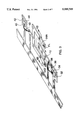
- FIG. 2A is a fragmentary perspective view of an embodiment of a lead frame for use in forming a lead frame capacitor in accordance with principles of the present invention
- FIG. 2B is a cross-sectional view of the lead frame of FIG. 2A, taken from line 2B--2B of FIG. 2A;
- FIG. 3 is a perspective view of the lead frame of FIGS. 2A-B after semiconductor die attachment and wire bonding;
- FIG. 4A is a fragmentary perspective view of the lead frame of FIG. 3 after encapsulation with dielectric molding material
- FIG. 4B is a cross-sectional view of the lead frame of FIG. 3, taken from line 4B--4B of FIG. 3, after encapsulation with dielectric molding material;
- FIG. 5 is a schematic block diagram of an embodiment of an isolator circuit incorporating a pair of lead frame capacitors in accordance with principles of the present invention
- FIG. 6 is a detailed block diagram of a low power digital isolator circuit constructed in accordance with principles of the present invention.
- FIG. 7 illustrates the various signal waveforms for the digital isolator circuit of FIG. 6.
- FIG. 8 is a plan view of an embodiment of a lead frame for the low power digital isolator circuit of FIG. 6.
- FIG. 1 is a schematic diagram providing a simplified illustration of a capacitor 10 made in accordance with the present invention.
- Capacitor 10 includes electrodes 12 and 14 embedded and separated from each other by dielectric material 16. Electrodes 12 and 14 are formed from portions of a lead frame structure of the type used in conventional integrated circuit assembly. Dielectric material 16 is formed from molding material of the type used for encapsulation in conventional integrated circuit plastic packages. In a typical isolator circuit application, electrodes 12 and 14 would be electrically connected by conventional wire bonding to different integrated circuit dies operating at different ground reference potentials.
- FIGS. 2-4 illustrate various aspects of an exemplary embodiment of capacitor 10.
- FIG. 2A is a fragmentary perspective view of a lead frame structure 30 configured to provide a capacitor in accordance with the present invention.
- lead frame structure 30 includes capacitor electrodes 12 and 14 and die attachment pads 32 and 42.
- Electrode 14 includes electrode fingers 14A and 14B, each of which is positioned to extend parallel to and on opposite sides of a single electrode finger of electrode 12.
- Portion 30A of lead frame structure 30 is a temporary support structure joining electrodes 12 and 14 and die attachment pads 32 and 42 during die attachment, wire bonding and encapsulation.
- Lead frame structure 30 can be adapted to provide electrodes 12 and 14 and die attachment pads 32 and 34 using conventional lead frame fabrication processes (e.g., stamping or etching).
- electrodes 12 and 14 will form a coplanar and interdigitated capacitor wherein fringing electric fields provide the capacitance between electrode finger 12 and each of electrode fingers 14A and 14B.
- One of the factors which determines the capacitance of capacitor 10 is the distance between the electrodes. This distance is illustrated in FIG. 2B, which shows a cross-sectional view of lead frame structure 30 of FIG. 2A, taken from line 2B--2B of FIG. 2.
- lead frame electrode fingers 14A and 14B are separated from lead frame electrode 12 by an electrode separation distance of "ES”.
- the distance "ES” along with other physical parameters relating to the size and shape of capacitor 10, are variables that can be easily controlled when fabricating lead frame structure 30 to achieve capacitors of different values and to meet the particular size constraints of conventional integrated circuit packages.
- FIG. 3 is a perspective view of the lead frame structure 30 of FIGS. 2A and 2B after semiconductor die attachment and wire bonding.
- semiconductor dies 34 and 44 are respectively attached to die attachment pads 32 and 42.
- a silver-filed epoxy may be used to provide a conductive attachment between the dies and their respective attachment pads.
- Semiconductor dies 34 and 44 include respective bonding pads 36 and 46 coupled to circuitry (not shown) on the dies.
- Wire bonds 38,48 are used to make electrical connections between semiconductor dies 34,44 and lead frame electrodes 12,14, respectively.
- semiconductor dies 34 and 44 will be capacitively coupled together through lead frame electrodes 12 and 14.
- the electrode fringe length "FL" see dashed line labelled "FL" that substantially contributes to determining the value of the capacitance of the lead frame capacitor.
- FIGS. 2-4 illustrate an embodiment of the lead frame capacitor of the present invention wherein the capacitor electrodes are coplanar and interdigitated.
- the capacitor electrodes form what is commonly referred to as a "fringe capacitor” due to the fringing electric fields that provide the capacitance.
- the capacitance value of capacitor 10 is determined substantially by the electrode separation distance "ES" (FIG. 2B), the electrode fringe length "FL" (FIG. 3) and the dielectric constant of dielectric molding material 40. (Assuming, of course, that the dielectric thickness "DT" [FIG. 4B] is significantly greater than the electrode separation distance "ES".)
- the electrode fringe length "FU" like the electrode separation distance "ES” can be easily controlled when fabricating lead frame structure 30 and can be varied as desired to achieve different capacitance values. As is well known, for example, increasing either the electrode fringe length "FL” or the dielectric constant of the dielectric molding material generally increases the value of the capacitance, whereas increasing the electrode separation distance "ED" generally decreases the value of the capacitance.
- lead frame capacitance values ranging at least from approximately 0.1 picofarad to 2 picofarad should be readily achievable within a conventional eighteen lead molded plastic dual-in-line (DIP) package (e.g., a package approximately 23 mm long by 6 mm wide by 3 mm high).
- DIP dual-in-line
- capacitor electrode shapes other than those shown in FIGS. 2-4 also can be formed in accordance with the present invention.
- the breakdown voltage of the lead frame capacitor of the present invention will be determined substantially by the electrode separation distance "ES" (FIG. 2B) and the dielectric properties of the dielectric molding material. For example, as the electrode separation distance increases, the breakdown voltage generally increases (although the lead frame capacitance accordingly decreases). Furthermore, as the breakdown strength of the dielectric molding material increases, the breakdown voltage of the capacitor also generally increases.
- the present invention can be used to achieve isolation voltages in excess of a thousand volts.
- a common type of plastic molding material used in injection molded plastic packages is novalak epoxy.
- Novalak is a thermoplastic phenolformaldehyde-type resin.
- a breakdown voltage in excess of 1000 volts can be obtained with this material.
- Lead frame structure 30 can be made from a conventional lead frame material.
- a conventional lead frame material For example, an iron-nickel-based alloy approximately 0.254 mm thick has been successfully used, although many other conducting materials and thickness could be used as well.
- the encapsulation material of the present invention can be a conventional molding material used in integrated circuit packaging (e.g., novalak epoxy having a dielectric constant of approximately 4), many other dielectric materials could be used as well. It is preferable that such dielectric materials have a high breakdown strength, high dielectric constant and low loss.
- FIGS. 2-4 illustrate that in order to fabricate the lead frame capacitor of the present invention, the following steps are carried out.
- Capacitor electrodes are first patterned into a single sheet of lead frame material. Electrical connections between the capacitor electrodes and circuitry on one or more integrated circuit chips are then made by wire bonding. Lastly, the capacitor electrodes are encapsulated with dielectric molding material to provide dielectric insulation between electrodes.
- a feature of the lead frame capacitor of the present invention is that each of the above steps are performed during the fabrication of conventional integrated circuits.
- the lead frame capacitor of the present invention can be provided in an integrated circuit at little or no additional cost and without added assembly or packaging complexity.
- FIG. 5 is a schematic block diagram of an embodiment 50 of an isolator circuit incorporating a pair of the lead frame capacitors of the present invention.
- Isolator circuit 50 includes circuit 62 (having terminals 62A, 62B and 62C) and circuit 64 (having terminals 64A, 64B and 64C).
- Circuit 50 also includes lead frame capacitors 52 and 54 encapsulated with dielectric molding material 56. Terminals 62A and 64A are capacitively coupled together through lead-frame capacitor 52, while terminals 62B and 64B are capacitively coupled together through lead-frame capacitor 54. Terminals 62C and 64C are connected to respective ground reference potentials GND1 and GND2.
- Circuits 62 and 64 may be of various types.
- circuit 62 could be a driver circuit for generating electrical signals to be capacitively coupled across lead frame capacitors 52 and 54.
- Circuit 64 could be a receiver circuit for receiving such signals.
- GND1 of driver 62 could be at a different potential than GND2 of receiver 64. Thus, such a circuit could provide isolation between respective circuits.
- circuits 62 and 64 could each be a transceiver circuit for both transmitting an electrical signal across lead frame capacitors 52 and 54 and for receiving such signals.
- GND1 of transceiver 62 could be at a different potential than GND2 of transceiver 64.
- FIG. 6 provides a more detailed block diagram of an exemplary embodiment of a low power digital isolator circuit 100 constructed in accordance with the principles of the present invention and which utilizes a pair of the lead frame capacitors discussed above.
- FIG. 7 illustrates the various signal waveforms for the digital isolator circuit of FIG. 6.
- Transmitter 110 includes gated oscillator 112 and drivers 114 and 116.
- the supply current for gated oscillator 112 and drivers 114,116 are provided through digital input 118.
- digital input (DIN) 118 exceeds a predetermined voltage (e.g., 3 volts)
- gated oscillator 112 turns on and provides a fixed-frequency square wave (at, for example, 4 MHz) to drivers 114 and 116 through driver inputs 114A and 116A, respectively.
- the outputs 114B and 116B of drivers 114 and 116 thus oscillate out of phase with each other at the same fixed frequency of gated oscillator 112. (See waveforms 118, 114B and 116B in FIG. 7, which illustrate the waveforms at terminals 118, 114B and 116 of FIG. 6, respectively.)
- Drivers 114 and 116 couple the fixed-frequency square wave signal from gated oscillator 112 through lead frame capacitors 105 and 115 and form differential signals at inputs 131 and 132 of comparator 130.
- Comparator 130 is a hysteretic comparator so as to prevent a change in output state until inputs 131 and 132 are significantly different in voltage.
- Comparator output 133 is used to drive input 134A of one-shot circuit 134.
- one-shot circuit output 134B coupled through TTL buffer 135, goes HIGH.
- the time constant of one-shot circuit 134 is set to a predetermined multiple (e.g., two) of the period of oscillation of oscillator 112. As a result, output signal 135A will stay HIGH as long as the oscillation continues.
- gated oscillator 112 of transmitter 110 turns OFF and one-shot circuit output signal 135A resets LOW.
- one-shot circuit output signal 135A substantially tracks digital input DIN independent of whether GND1 is at a same or different potential than GND2.
- This feature of the present invention is provided by lead frame capacitors 105 and 115 which supply an isolation barrier in isolator circuit 100.
- an optional filter 136 is preferably added to receiver circuit 120.
- Filter 136 is a binary counter clocked by either an internal free running oscillator 140 or an external oscillator (not shown) coupled to isolator circuit 100 through external oscillator input 148.
- Clock detector circuit 145 decouples internal oscillator 140 from filter 136 and couples the external oscillator (through switches 146 and 147, respectively) after detecting, for example, three consecutive pulses on external oscillator input 148. (Waveform 136A, shown in FIG. 7, illustrates the oscillation waveform at input 136A of filter 136.)
- the frequency of internal oscillator 140 is preferably designed to match the frequency (although not synchronized) of gated oscillator 112 in transmitter 110.
- filter 136 For digital output DOUT 138A (through TTL buffer 138) to go HIGH, filter 136 must count a predetermined number of consecutive clock cycles (for example, four) with one-shot circuit output 134B remaining HIGH.
- filter 136 For digital output DOUT 138A (through TTL buffer 138) to go LOW, filter 136 must also count a predetermined number of consecutive clock cycles (for example, four) with one-shot circuit output 134B remaining LOW.
- Waveform DOUT 138A shown in FIG. 7, illustrates how data output 138A goes HIGH and returns LOW after four consecutive clock cycles. (The shaded areas in waveform DOUT 138A are due to oscillator 112 not being synchronized with oscillator input 136A of filter 136.)
- filter 136 provides enhanced noise and glitch immunity to isolator circuit 100.
- the digital input DIN 118 is LOW and gated oscillator 112 is OFF and there is a very large fast-rising common mode signal at ground GND1 110A and input DIN 118 (i.e., DIN is tied to GND1) with respect to ground GND2 of receiver 120. Any mismatch in lead-frame capacitors 105 and 115 will convert the common mode signal into a differential glitch at inputs 131 and 132 of comparator 130.
- FIG. 6 is a plan view of an embodiment of a preferred lead frame 150, after die attachment and wire bonding, for the low power digital isolator circuit of FIGS. 6 and 7.
- Lead frame 150 has a size which corresponds to the size of the lead frame in a conventional eighteen lead dual-in-line (DIP) package (e.g., approximately 23 mm long by 6 mm wide), except that it has ten (five on each side) of its center leads replaced to provide area for the lead frame capacitors.
- DIP lead dual-in-line
- transmitter 110 is manufactured on semiconductor die 151 which is attached to die pad 153 of lead frame 150.
- receiver circuit 120 is manufactured on semiconductor die 152 which is attached to die pad 154 of lead frame 150.
- Lead frame 150 also includes interdigitated fingers 156A, 156B and 157, for forming lead-frame capacitor 105, and interdigitated fingers 166A, 166B and 167, for forming lead-frame capacitor 115.
- Lead frame 150 also includes regions 165 which are removed after the complete isolator circuit is encapsulated with dielectric molding material so as to allow package pins 170 to be electrically isolated from each other. Locking holes 160 are included on lead frame 150 so as to allow the dielectric molding material to firmly hold package pins 170 in place during user handling.
- the circuit preferably uses low cost capacitors incorporated into the lead frame of a conventional integrated circuit package. Using conventional dielectric molding materials, the circuit can provide up to 1000 volts of isolation from input to output for TTL digital signals. Input currents as low as 60 and 600 microamps are achievable for embodiments which can handle frequencies of up to 20 and 200 kps, respectively.
Landscapes
- Lead Frames For Integrated Circuits (AREA)
- Semiconductor Integrated Circuits (AREA)
Abstract
Description
Claims (17)
Priority Applications (1)
| Application Number | Priority Date | Filing Date | Title |
|---|---|---|---|
| US08/401,027 US5589709A (en) | 1992-12-03 | 1995-03-08 | Lead frame capacitor and capacitively-coupled isolator circuit using same |
Applications Claiming Priority (2)
| Application Number | Priority Date | Filing Date | Title |
|---|---|---|---|
| US07/985,881 US5444600A (en) | 1992-12-03 | 1992-12-03 | Lead frame capacitor and capacitively-coupled isolator circuit using the same |
| US08/401,027 US5589709A (en) | 1992-12-03 | 1995-03-08 | Lead frame capacitor and capacitively-coupled isolator circuit using same |
Related Parent Applications (1)
| Application Number | Title | Priority Date | Filing Date |
|---|---|---|---|
| US07/985,881 Division US5444600A (en) | 1992-12-03 | 1992-12-03 | Lead frame capacitor and capacitively-coupled isolator circuit using the same |
Publications (1)
| Publication Number | Publication Date |
|---|---|
| US5589709A true US5589709A (en) | 1996-12-31 |
Family
ID=25531882
Family Applications (5)
| Application Number | Title | Priority Date | Filing Date |
|---|---|---|---|
| US07/985,881 Expired - Lifetime US5444600A (en) | 1992-12-03 | 1992-12-03 | Lead frame capacitor and capacitively-coupled isolator circuit using the same |
| US08/401,028 Expired - Lifetime US5926358A (en) | 1992-12-03 | 1995-03-08 | Lead frame capacitor and capacitively-coupled isolator circuit using same |
| US08/401,033 Expired - Lifetime US5650357A (en) | 1992-12-03 | 1995-03-08 | Process for manufacturing a lead frame capacitor and capacitively-coupled isolator circuit using same |
| US08/401,027 Expired - Lifetime US5589709A (en) | 1992-12-03 | 1995-03-08 | Lead frame capacitor and capacitively-coupled isolator circuit using same |
| US08/807,197 Expired - Lifetime US5945728A (en) | 1992-12-03 | 1997-02-27 | Lead frame capacitor and capacitively coupled isolator circuit |
Family Applications Before (3)
| Application Number | Title | Priority Date | Filing Date |
|---|---|---|---|
| US07/985,881 Expired - Lifetime US5444600A (en) | 1992-12-03 | 1992-12-03 | Lead frame capacitor and capacitively-coupled isolator circuit using the same |
| US08/401,028 Expired - Lifetime US5926358A (en) | 1992-12-03 | 1995-03-08 | Lead frame capacitor and capacitively-coupled isolator circuit using same |
| US08/401,033 Expired - Lifetime US5650357A (en) | 1992-12-03 | 1995-03-08 | Process for manufacturing a lead frame capacitor and capacitively-coupled isolator circuit using same |
Family Applications After (1)
| Application Number | Title | Priority Date | Filing Date |
|---|---|---|---|
| US08/807,197 Expired - Lifetime US5945728A (en) | 1992-12-03 | 1997-02-27 | Lead frame capacitor and capacitively coupled isolator circuit |
Country Status (4)
| Country | Link |
|---|---|
| US (5) | US5444600A (en) |
| EP (1) | EP0600488B1 (en) |
| JP (1) | JP2690264B2 (en) |
| DE (1) | DE69332140T2 (en) |
Cited By (12)
| Publication number | Priority date | Publication date | Assignee | Title |
|---|---|---|---|---|
| US5939766A (en) * | 1996-07-24 | 1999-08-17 | Advanced Micro Devices, Inc. | High quality capacitor for sub-micrometer integrated circuits |
| US6084285A (en) * | 1997-10-20 | 2000-07-04 | The Board Of Trustees Of The Leland Stanford Junior University | Lateral flux capacitor having fractal-shaped perimeters |
| US6300617B1 (en) | 1998-03-04 | 2001-10-09 | Nonvolatile Electronics, Incorporated | Magnetic digital signal coupler having selected/reversal directions of magnetization |
| US6362972B1 (en) | 2000-04-13 | 2002-03-26 | Molex Incorporated | Contactless interconnection system |
| US6612852B1 (en) | 2000-04-13 | 2003-09-02 | Molex Incorporated | Contactless interconnection system |
| US20060061350A1 (en) * | 2004-09-17 | 2006-03-23 | Nve Corporation | Inverted magnetic isolator |
| US20080278256A1 (en) * | 2007-05-11 | 2008-11-13 | Intersil Americas Inc. | Rf - coupled digital isolator |
| US8497700B2 (en) | 2011-10-21 | 2013-07-30 | Samsung Electro-Mechanics | Systems and methods for propagating digital data across an isolation barrier |
| CN103617992A (en) * | 2013-11-27 | 2014-03-05 | 苏州贝克微电子有限公司 | Lead frame capacitor and capacitive coupling isolator circuit |
| US20140162575A1 (en) * | 2012-12-07 | 2014-06-12 | Anayas360.Com, Llc | Highly integrated millimeter-wave soc layout techniques for improved performance and modeling accuracy |
| US9257834B1 (en) | 2015-02-13 | 2016-02-09 | The Silanna Group Pty Ltd. | Single-laminate galvanic isolator assemblies |
| TWI642147B (en) * | 2018-01-29 | 2018-11-21 | 新加坡商光寶新加坡有限公司 | Capacitor coupling package structure for capacitive coupling isolator |
Families Citing this family (95)
| Publication number | Priority date | Publication date | Assignee | Title |
|---|---|---|---|---|
| US5444600A (en) * | 1992-12-03 | 1995-08-22 | Linear Technology Corporation | Lead frame capacitor and capacitively-coupled isolator circuit using the same |
| EP0650739B1 (en) | 1993-10-28 | 2003-02-26 | Medrad, Inc. | Total system for contrast delivery |
| US5491360A (en) * | 1994-12-28 | 1996-02-13 | National Semiconductor Corporation | Electronic package for isolated circuits |
| JP3565991B2 (en) * | 1996-06-26 | 2004-09-15 | 株式会社ルネサステクノロジ | Semiconductor integrated circuit and method of manufacturing semiconductor integrated circuit |
| DE19639369A1 (en) * | 1996-09-25 | 1998-03-26 | Philips Patentverwaltung | Circuit board |
| US6137827A (en) * | 1997-04-22 | 2000-10-24 | Silicon Laboratories, Inc. | Isolation system with digital communication across a capacitive barrier |
| US5982018A (en) | 1997-05-23 | 1999-11-09 | Micron Technology, Inc. | Thin film capacitor coupons for memory modules and multi-chip modules |
| US20030042571A1 (en) * | 1997-10-23 | 2003-03-06 | Baoxing Chen | Chip-scale coils and isolators based thereon |
| US6054908A (en) * | 1997-12-12 | 2000-04-25 | Trw Inc. | Variable bandwidth filter |
| US6268643B1 (en) * | 1997-12-22 | 2001-07-31 | Texas Instruments Incorporated | Lead frame device for delivering electrical power to a semiconductor die |
| DE19805785C1 (en) * | 1998-02-12 | 1999-06-17 | Siemens Ag | Power semiconductor module having temperature dependent lead breaking material |
| KR19990072936A (en) | 1998-02-27 | 1999-09-27 | 가나이 쓰도무 | Isolator and modem unit using the same |
| US6114756A (en) | 1998-04-01 | 2000-09-05 | Micron Technology, Inc. | Interdigitated capacitor design for integrated circuit leadframes |
| KR100294449B1 (en) * | 1998-07-15 | 2001-07-12 | 윤종용 | Semiconductor integrated circuit device with capacitor formed under bonding pad |
| US6087882A (en) * | 1998-12-04 | 2000-07-11 | Analog Devices, Inc. | Ultra-low power magnetically coupled digital isolator using spin valve resistors |
| US6351033B1 (en) * | 1999-10-06 | 2002-02-26 | Agere Systems Guardian Corp. | Multifunction lead frame and integrated circuit package incorporating the same |
| KR20030084256A (en) * | 2002-04-26 | 2003-11-01 | 삼화전기주식회사 | Solid state electrolytic capacitor and lead frame used therefor |
| DE10243197B4 (en) | 2002-09-18 | 2011-05-05 | Infineon Technologies Ag | Digital signal transmission method |
| JP3916072B2 (en) * | 2003-02-04 | 2007-05-16 | 住友電気工業株式会社 | AC coupling circuit |
| US6880134B2 (en) * | 2003-04-09 | 2005-04-12 | Freescale Semiconductor, Inc. | Method for improving capacitor noise and mismatch constraints in a semiconductor device |
| EP1618712A2 (en) * | 2003-04-30 | 2006-01-25 | Analog Devices, Inc. | Signal isolators using micro-transformers |
| US7253506B2 (en) * | 2003-06-23 | 2007-08-07 | Power-One, Inc. | Micro lead frame package |
| US7307502B2 (en) * | 2003-07-16 | 2007-12-11 | Marvell World Trade Ltd. | Power inductor with reduced DC current saturation |
| US7023313B2 (en) * | 2003-07-16 | 2006-04-04 | Marvell World Trade Ltd. | Power inductor with reduced DC current saturation |
| US7489219B2 (en) * | 2003-07-16 | 2009-02-10 | Marvell World Trade Ltd. | Power inductor with reduced DC current saturation |
| US7872454B2 (en) * | 2003-08-21 | 2011-01-18 | Marvell World Trade Ltd. | Digital low dropout regulator |
| US7760525B2 (en) * | 2003-08-21 | 2010-07-20 | Marvell World Trade Ltd. | Voltage regulator |
| US6929485B1 (en) * | 2004-03-16 | 2005-08-16 | Agilent Technologies, Inc. | Lead frame with interdigitated pins |
| US8324872B2 (en) * | 2004-03-26 | 2012-12-04 | Marvell World Trade, Ltd. | Voltage regulator with coupled inductors having high coefficient of coupling |
| US7447492B2 (en) * | 2004-06-03 | 2008-11-04 | Silicon Laboratories Inc. | On chip transformer isolator |
| US8169108B2 (en) * | 2004-06-03 | 2012-05-01 | Silicon Laboratories Inc. | Capacitive isolator |
| US8198951B2 (en) * | 2004-06-03 | 2012-06-12 | Silicon Laboratories Inc. | Capacitive isolation circuitry |
| US7577223B2 (en) | 2004-06-03 | 2009-08-18 | Silicon Laboratories Inc. | Multiplexed RF isolator circuit |
| US7821428B2 (en) | 2004-06-03 | 2010-10-26 | Silicon Laboratories Inc. | MCU with integrated voltage isolator and integrated galvanically isolated asynchronous serial data link |
| US7460604B2 (en) * | 2004-06-03 | 2008-12-02 | Silicon Laboratories Inc. | RF isolator for isolating voltage sensing and gate drivers |
| US7421028B2 (en) * | 2004-06-03 | 2008-09-02 | Silicon Laboratories Inc. | Transformer isolator for digital power supply |
| US8441325B2 (en) | 2004-06-03 | 2013-05-14 | Silicon Laboratories Inc. | Isolator with complementary configurable memory |
| US7302247B2 (en) * | 2004-06-03 | 2007-11-27 | Silicon Laboratories Inc. | Spread spectrum isolator |
| US7738568B2 (en) * | 2004-06-03 | 2010-06-15 | Silicon Laboratories Inc. | Multiplexed RF isolator |
| US7737871B2 (en) | 2004-06-03 | 2010-06-15 | Silicon Laboratories Inc. | MCU with integrated voltage isolator to provide a galvanic isolation between input and output |
| US7902627B2 (en) | 2004-06-03 | 2011-03-08 | Silicon Laboratories Inc. | Capacitive isolation circuitry with improved common mode detector |
| US7376212B2 (en) * | 2004-06-03 | 2008-05-20 | Silicon Laboratories Inc. | RF isolator with differential input/output |
| US7190152B2 (en) * | 2004-07-13 | 2007-03-13 | Marvell World Trade Ltd. | Closed-loop digital control system for a DC/DC converter |
| US7535262B2 (en) | 2004-10-19 | 2009-05-19 | International Rectifier Corporation | High voltage level shifting by capacitive coupling |
| US7761719B2 (en) * | 2005-03-28 | 2010-07-20 | Akros Silicon Inc. | Ethernet module |
| US7719305B2 (en) * | 2006-07-06 | 2010-05-18 | Analog Devices, Inc. | Signal isolator using micro-transformers |
| US8093983B2 (en) * | 2006-08-28 | 2012-01-10 | Avago Technologies Ecbu Ip (Singapore) Pte. Ltd. | Narrowbody coil isolator |
| US9105391B2 (en) | 2006-08-28 | 2015-08-11 | Avago Technologies General Ip (Singapore) Pte. Ltd. | High voltage hold-off coil transducer |
| US7960845B2 (en) | 2008-01-03 | 2011-06-14 | Linear Technology Corporation | Flexible contactless wire bonding structure and methodology for semiconductor device |
| US8089311B2 (en) * | 2008-01-22 | 2012-01-03 | Analog Devices, Inc. | Signal amplifier |
| US8084894B2 (en) * | 2008-02-04 | 2011-12-27 | Analog Devices, Inc. | Solid state relay |
| US7741896B2 (en) * | 2008-02-15 | 2010-06-22 | Avago Technologies Ecbu Ip (Singapore) Pte. Ltd. | High voltage drive circuit employing capacitive signal coupling and associated devices and methods |
| US7741935B2 (en) * | 2008-02-15 | 2010-06-22 | Avago Technologies Ecbu Ip (Singapore) Pte. Ltd. | High voltage isolation semiconductor capacitor digital communication device and corresponding package |
| US8188814B2 (en) * | 2008-02-15 | 2012-05-29 | Avago Technologies Ecbu Ip (Singapore) Pte. Ltd. | High voltage isolation dual capacitor communication system |
| US7983059B2 (en) * | 2008-09-02 | 2011-07-19 | Analog Devices, Inc. | High frequency power converter based on transformers |
| US7902665B2 (en) * | 2008-09-02 | 2011-03-08 | Linear Technology Corporation | Semiconductor device having a suspended isolating interconnect |
| US8582669B2 (en) * | 2008-10-30 | 2013-11-12 | Analog Devices, Inc. | Noise reduction circuit in a digital isolator system |
| US8902016B2 (en) | 2009-10-21 | 2014-12-02 | Stmicroelectronics S.R.L. | Signal transmission through LC resonant circuits |
| US8791711B2 (en) * | 2009-10-21 | 2014-07-29 | Stmicroelectronics S.R.L. | Testing of electronic devices through capacitive interface |
| US8451032B2 (en) | 2010-12-22 | 2013-05-28 | Silicon Laboratories Inc. | Capacitive isolator with schmitt trigger |
| US9087713B2 (en) | 2012-10-12 | 2015-07-21 | Power Integrations, Inc. | Semiconductor device with shared region |
| US8976561B2 (en) | 2012-11-14 | 2015-03-10 | Power Integrations, Inc. | Switch mode power converters using magnetically coupled galvanically isolated lead frame communication |
| US9035435B2 (en) | 2012-11-14 | 2015-05-19 | Power Integrations, Inc. | Magnetically coupled galvanically isolated communication using lead frame |
| US8818296B2 (en) | 2012-11-14 | 2014-08-26 | Power Integrations, Inc. | Noise cancellation for a magnetically coupled communication link utilizing a lead frame |
| US9276479B2 (en) | 2013-01-22 | 2016-03-01 | Power Integrations, Inc. | Receive circuit for use in a power converter |
| US9331587B2 (en) | 2013-01-22 | 2016-05-03 | Power Integrations, Inc. | Power converter controller with multiple power sources |
| US9178411B2 (en) | 2013-01-22 | 2015-11-03 | Power Integrations, Inc. | Charging circuit for a power converter controller |
| US9374011B2 (en) | 2013-01-22 | 2016-06-21 | Power Integrations, Inc. | Secondary controller for use in synchronous flyback converter |
| US9166486B2 (en) | 2013-03-08 | 2015-10-20 | Power Integrations, Inc. | Power converter using multiple controllers |
| US9019728B2 (en) | 2013-03-08 | 2015-04-28 | Power Integrations, Inc. | Power converter output voltage clamp and supply terminal |
| US9136765B2 (en) | 2013-03-08 | 2015-09-15 | Power Integrations, Inc. | Techniques for controlling a power converter using multiple controllers |
| US9166575B2 (en) | 2013-03-08 | 2015-10-20 | Power Integrations, Inc. | Low threshold voltage comparator |
| US9337253B2 (en) * | 2013-03-09 | 2016-05-10 | Microchip Technology Incorporated | Method and apparatus for constructing an isolation capacitor in an integrated circuit |
| US9071146B2 (en) | 2013-03-13 | 2015-06-30 | Power Integrations, Inc. | AC voltage sensor with low power consumption |
| US9401657B2 (en) | 2013-03-13 | 2016-07-26 | Power Integrations, Inc. | Input voltage sensor responsive to load conditions |
| US9246392B2 (en) | 2013-03-13 | 2016-01-26 | Power Integrations, Inc. | Switched mode power converter controller with ramp time modulation |
| US9293997B2 (en) | 2013-03-14 | 2016-03-22 | Analog Devices Global | Isolated error amplifier for isolated power supplies |
| US9496926B2 (en) | 2013-05-24 | 2016-11-15 | Texas Instruments Incorporated | Galvanic isolator |
| CN103280442A (en) * | 2013-05-27 | 2013-09-04 | 苏州贝克微电子有限公司 | Capacitors using same lead frame and capacitive coupling isolating circuit |
| US10536309B2 (en) | 2014-09-15 | 2020-01-14 | Analog Devices, Inc. | Demodulation of on-off-key modulated signals in signal isolator systems |
| US9660848B2 (en) | 2014-09-15 | 2017-05-23 | Analog Devices Global | Methods and structures to generate on/off keyed carrier signals for signal isolators |
| US10270630B2 (en) | 2014-09-15 | 2019-04-23 | Analog Devices, Inc. | Demodulation of on-off-key modulated signals in signal isolator systems |
| US9998301B2 (en) | 2014-11-03 | 2018-06-12 | Analog Devices, Inc. | Signal isolator system with protection for common mode transients |
| EP3293889B1 (en) | 2016-09-13 | 2019-02-27 | Allegro MicroSystems, LLC | Signal isolator having bidirectional diagnostic signal exchange |
| JP6923248B2 (en) * | 2017-03-31 | 2021-08-18 | 新日本無線株式会社 | Semiconductor device |
| US10243442B1 (en) | 2017-11-22 | 2019-03-26 | Power Integrations, Inc. | Controller with frequency to on-time converter |
| CN111801842B (en) * | 2018-03-07 | 2022-03-22 | 住友电工光电子器件创新株式会社 | Semiconductor device with a plurality of semiconductor chips |
| US11115244B2 (en) | 2019-09-17 | 2021-09-07 | Allegro Microsystems, Llc | Signal isolator with three state data transmission |
| US11205611B1 (en) | 2020-06-15 | 2021-12-21 | Texas Instruments Incorporated | Leadframe capacitors |
| CN112039517B (en) * | 2020-09-04 | 2024-03-22 | 上海川土微电子有限公司 | Ultra-low power consumption capacitive digital isolator circuit based on Pulse-Coding |
| US12356552B2 (en) * | 2021-06-25 | 2025-07-08 | Intel Corporation | Capacitor formed with coupled dies |
| CN114823611A (en) * | 2021-08-17 | 2022-07-29 | 重庆线易电子科技有限责任公司 | Isolator and electronic component |
| CN114121864A (en) * | 2021-10-20 | 2022-03-01 | 上海闻泰信息技术有限公司 | System-in-package structure and manufacturing method thereof |
| CN114121865A (en) * | 2021-10-20 | 2022-03-01 | 上海闻泰信息技术有限公司 | System-in-package structure and manufacturing method thereof |
| CN115768198B (en) * | 2022-11-10 | 2024-09-06 | 昆山国显光电有限公司 | Display panel and display device |
Citations (65)
| Publication number | Priority date | Publication date | Assignee | Title |
|---|---|---|---|---|
| US2600343A (en) * | 1948-10-07 | 1952-06-10 | Kenyon Instr Company Inc | Method of making conductive patterns |
| US2777110A (en) * | 1952-10-07 | 1957-01-08 | Sprague Electric Co | Miniature high dielectric multicapacitor unit |
| US2885601A (en) * | 1954-05-28 | 1959-05-05 | Rca Corp | Insulation of printed circuits |
| US2896028A (en) * | 1954-09-30 | 1959-07-21 | Rca Corp | Printed circuit for high frequency amplifier apparatus |
| US3104377A (en) * | 1958-04-02 | 1963-09-17 | Itt | Storage device |
| US3168704A (en) * | 1961-03-06 | 1965-02-02 | Clevite Corp | Multivibrator amplifier with time delay modulating audio input |
| DE1197561B (en) * | 1960-09-21 | 1965-07-29 | Ass Elect Ind | Solid-state electrical component |
| US3264569A (en) * | 1964-12-07 | 1966-08-02 | Tia Electric Company | Transiently regenerative amplifier with a. c. and d. c. regeneration |
| US3316458A (en) * | 1965-01-29 | 1967-04-25 | Hughes Aircraft Co | Electronic circuit assembly with recessed substrate mounting means |
| US3437943A (en) * | 1965-03-16 | 1969-04-08 | Leeds & Northrup Co | Synchronized modulator-demodulator system |
| US3489952A (en) * | 1967-05-15 | 1970-01-13 | Singer Co | Encapsulated microelectronic devices |
| US3537022A (en) * | 1968-01-10 | 1970-10-27 | Hewlett Packard Co | Signal translating circuit |
| US3593208A (en) * | 1969-03-17 | 1971-07-13 | Bell Telephone Labor Inc | Microwave quadrature coupler having lumped-element capacitors |
| US3614832A (en) * | 1966-03-09 | 1971-10-26 | Ibm | Decal connectors and methods of forming decal connections to solid state devices |
| DE2114940A1 (en) * | 1970-09-21 | 1972-03-23 | Mess & Regelungst Veb K | Circuit arrangement for high-resistance DC voltage amplifiers |
| US3675095A (en) * | 1971-06-10 | 1972-07-04 | Rca Corp | Capacitors of constant capacitance |
| US3679941A (en) * | 1969-09-22 | 1972-07-25 | Gen Electric | Composite integrated circuits including semiconductor chips mounted on a common substrate with connections made through a dielectric encapsulator |
| US3714540A (en) * | 1970-11-10 | 1973-01-30 | Oxy Metal Finishing Corp | Isolation and transforming circuit |
| US3745508A (en) * | 1972-05-25 | 1973-07-10 | Bourns Inc | Selectable fixed impedance device |
| US3757175A (en) * | 1971-01-06 | 1973-09-04 | Soo Kim Chang | Tor chips mounted on a single substrate composite integrated circuits with coplnaar connections to semiconduc |
| US3764938A (en) * | 1972-08-28 | 1973-10-09 | Bell Telephone Labor Inc | Resonance suppression in interdigital capacitors useful as dc bias breaks in diode oscillator circuits |
| US3833838A (en) * | 1972-11-13 | 1974-09-03 | A Christiansen | Electronic component mounting wafers for repeated connection in a variety of circuit designs |
| GB1469944A (en) * | 1975-04-21 | 1977-04-06 | Decca Ltd | Planar capacitor |
| US4023053A (en) * | 1974-12-16 | 1977-05-10 | Tokyo Shibaura Electric Co., Ltd. | Variable capacity diode device |
| US4038488A (en) * | 1975-05-12 | 1977-07-26 | Cambridge Memories, Inc. | Multilayer ceramic multi-chip, dual in-line packaging assembly |
| US4117411A (en) * | 1977-09-26 | 1978-09-26 | Moore Products Co. | Isolation circuit with duty cycle feedback |
| DE2723363A1 (en) * | 1977-05-24 | 1978-11-30 | Philips Patentverwaltung | Capacitor with cylindrical dielectric former and conducting elements - has geometrically shaped dividing line separating tracks deposited by standardised process for mass prodn. |
| US4143508A (en) * | 1975-06-19 | 1979-03-13 | Citizen Watch Co. Ltd. | Electronic circuit block |
| US4167647A (en) * | 1974-10-02 | 1979-09-11 | Santa Barbara Research Center | Hybrid microelectronic circuit package |
| US4173033A (en) * | 1975-12-04 | 1979-10-30 | Daikin Kogyo Co., Ltd. | Polymeric dielectric for capacitors and the like consisting essentially of a vinylidene fluoride-trifluoroethylene copolymer |
| US4178556A (en) * | 1977-04-22 | 1979-12-11 | Attwood Brian E | Class D amplifier system |
| US4188651A (en) * | 1978-03-27 | 1980-02-12 | Sprague Electric Company | Ceramic capacitor with surface electrodes |
| US4193028A (en) * | 1978-05-05 | 1980-03-11 | Honeywell Inc. | Eddy current instrumentation circuitry for distinguishing flaw signals from spurious noise signals |
| US4249135A (en) * | 1980-03-25 | 1981-02-03 | Fisher Charles B | Amplifier with switched capacitors |
| US4292595A (en) * | 1979-11-13 | 1981-09-29 | Burr-Brown Research Corporation | Capacitance coupled isolation amplifier and method |
| US4376274A (en) * | 1980-10-01 | 1983-03-08 | Communications Patents Limited | Printed circuit transformers |
| US4391531A (en) * | 1980-12-19 | 1983-07-05 | Timex Corporation | Electrooptical display/lead frame subassembly and timepiece module including same |
| SU1048485A1 (en) * | 1982-05-13 | 1983-10-15 | Предприятие П/Я В-2119 | Operational amplifier |
| US4410905A (en) * | 1981-08-14 | 1983-10-18 | Amp Incorporated | Power, ground and decoupling structure for chip carriers |
| JPS58197862A (en) * | 1982-05-14 | 1983-11-17 | Nec Corp | Hermetic package for semiconductor device |
| US4506108A (en) * | 1983-04-01 | 1985-03-19 | Sperry Corporation | Copper body power hybrid package and method of manufacture |
| US4536638A (en) * | 1982-09-30 | 1985-08-20 | Witold Krynicki | Chip assembly |
| US4551747A (en) * | 1982-10-05 | 1985-11-05 | Mayo Foundation | Leadless chip carrier apparatus providing for a transmission line environment and improved heat dissipation |
| US4561039A (en) * | 1981-04-27 | 1985-12-24 | Alps Electric Co., Ltd. | Thick film electronic circuit |
| US4600907A (en) * | 1985-03-07 | 1986-07-15 | Tektronix, Inc. | Coplanar microstrap waveguide interconnector and method of interconnection |
| US4622619A (en) * | 1985-03-13 | 1986-11-11 | Rogers Corporation | Decoupling capacitor and method of manufacture thereof |
| JPS62108553A (en) * | 1985-11-06 | 1987-05-19 | Nec Corp | Resin seal type semiconductor device |
| US4680613A (en) * | 1983-12-01 | 1987-07-14 | Fairchild Semiconductor Corporation | Low impedance package for integrated circuit die |
| US4697858A (en) * | 1986-02-07 | 1987-10-06 | National Semiconductor Corporation | Active bus backplane |
| US4705917A (en) * | 1985-08-27 | 1987-11-10 | Hughes Aircraft Company | Microelectronic package |
| US4748419A (en) * | 1986-04-28 | 1988-05-31 | Burr-Brown Corporation | Isolation amplifier with precise timing of signals coupled across isolation barrier |
| US4780795A (en) * | 1986-04-28 | 1988-10-25 | Burr-Brown Corporation | Packages for hybrid integrated circuit high voltage isolation amplifiers and method of manufacture |
| US4835486A (en) * | 1986-04-28 | 1989-05-30 | Burr-Brown Corporation | Isolation amplifier with precise timing of signals coupled across isolation barrier |
| JPH02238655A (en) * | 1989-03-10 | 1990-09-20 | Nec Corp | Semiconductor package |
| US4974054A (en) * | 1988-02-24 | 1990-11-27 | Hitachi, Ltd. | Resin molded semiconductor device |
| DE3915998A1 (en) * | 1989-05-17 | 1990-11-29 | Vdo Schindling | Electronic component with integrated circuit - has voltage supply strip lines coupled each to capacitor electrode |
| JPH02294061A (en) * | 1989-05-08 | 1990-12-05 | Nippondenso Co Ltd | Multi chip package structure |
| US4991001A (en) * | 1988-03-31 | 1991-02-05 | Kabushiki Kaisha Toshiba | IC packing device with impedance adjusting insulative layer |
| JPH0378248A (en) * | 1989-08-22 | 1991-04-03 | Seiko Instr Inc | Semiconductor device |
| US5057805A (en) * | 1990-05-16 | 1991-10-15 | Mitsubishi Denki Kabushiki Kaisha | Microwave semiconductor device |
| JPH0444242A (en) * | 1990-06-07 | 1992-02-14 | Fuji Electric Co Ltd | Manufacture of semiconductor device |
| JPH04162657A (en) * | 1990-10-26 | 1992-06-08 | Hitachi Ltd | Lead frame for semiconductor device |
| US5223220A (en) * | 1990-03-27 | 1993-06-29 | Pacific Biotech, Inc. | Solid phase immunoassay device and method of making same |
| US5229640A (en) * | 1992-09-01 | 1993-07-20 | Avx Corporation | Surface mountable clock oscillator module |
| US5302921A (en) * | 1991-05-31 | 1994-04-12 | Seiko Epson Corporation | Piezoelectric oscillator having reduced radiation of higher harmonics |
Family Cites Families (5)
| Publication number | Priority date | Publication date | Assignee | Title |
|---|---|---|---|---|
| JPS58197962A (en) * | 1982-05-13 | 1983-11-17 | Matsushita Electric Ind Co Ltd | Synchronizing device |
| FR2598032B1 (en) * | 1986-04-28 | 1991-08-09 | Burr Brown Corp | HYBRID INTEGRATED CIRCUIT FOR INSULATION AMPLIFIER |
| JP2714056B2 (en) * | 1988-10-19 | 1998-02-16 | キヤノン株式会社 | Ink jet recording apparatus capable of detachably attaching waste ink container and waste ink container used therein |
| US5233220A (en) * | 1989-06-30 | 1993-08-03 | Texas Instruments Incorporated | Balanced capacitance lead frame for integrated circuits and integrated circuit device with separate conductive layer |
| US5444600A (en) * | 1992-12-03 | 1995-08-22 | Linear Technology Corporation | Lead frame capacitor and capacitively-coupled isolator circuit using the same |
-
1992
- 1992-12-03 US US07/985,881 patent/US5444600A/en not_active Expired - Lifetime
-
1993
- 1993-12-02 DE DE69332140T patent/DE69332140T2/en not_active Expired - Lifetime
- 1993-12-02 EP EP93119453A patent/EP0600488B1/en not_active Expired - Lifetime
- 1993-12-03 JP JP5304235A patent/JP2690264B2/en not_active Expired - Lifetime
-
1995
- 1995-03-08 US US08/401,028 patent/US5926358A/en not_active Expired - Lifetime
- 1995-03-08 US US08/401,033 patent/US5650357A/en not_active Expired - Lifetime
- 1995-03-08 US US08/401,027 patent/US5589709A/en not_active Expired - Lifetime
-
1997
- 1997-02-27 US US08/807,197 patent/US5945728A/en not_active Expired - Lifetime
Patent Citations (65)
| Publication number | Priority date | Publication date | Assignee | Title |
|---|---|---|---|---|
| US2600343A (en) * | 1948-10-07 | 1952-06-10 | Kenyon Instr Company Inc | Method of making conductive patterns |
| US2777110A (en) * | 1952-10-07 | 1957-01-08 | Sprague Electric Co | Miniature high dielectric multicapacitor unit |
| US2885601A (en) * | 1954-05-28 | 1959-05-05 | Rca Corp | Insulation of printed circuits |
| US2896028A (en) * | 1954-09-30 | 1959-07-21 | Rca Corp | Printed circuit for high frequency amplifier apparatus |
| US3104377A (en) * | 1958-04-02 | 1963-09-17 | Itt | Storage device |
| DE1197561B (en) * | 1960-09-21 | 1965-07-29 | Ass Elect Ind | Solid-state electrical component |
| US3168704A (en) * | 1961-03-06 | 1965-02-02 | Clevite Corp | Multivibrator amplifier with time delay modulating audio input |
| US3264569A (en) * | 1964-12-07 | 1966-08-02 | Tia Electric Company | Transiently regenerative amplifier with a. c. and d. c. regeneration |
| US3316458A (en) * | 1965-01-29 | 1967-04-25 | Hughes Aircraft Co | Electronic circuit assembly with recessed substrate mounting means |
| US3437943A (en) * | 1965-03-16 | 1969-04-08 | Leeds & Northrup Co | Synchronized modulator-demodulator system |
| US3614832A (en) * | 1966-03-09 | 1971-10-26 | Ibm | Decal connectors and methods of forming decal connections to solid state devices |
| US3489952A (en) * | 1967-05-15 | 1970-01-13 | Singer Co | Encapsulated microelectronic devices |
| US3537022A (en) * | 1968-01-10 | 1970-10-27 | Hewlett Packard Co | Signal translating circuit |
| US3593208A (en) * | 1969-03-17 | 1971-07-13 | Bell Telephone Labor Inc | Microwave quadrature coupler having lumped-element capacitors |
| US3679941A (en) * | 1969-09-22 | 1972-07-25 | Gen Electric | Composite integrated circuits including semiconductor chips mounted on a common substrate with connections made through a dielectric encapsulator |
| DE2114940A1 (en) * | 1970-09-21 | 1972-03-23 | Mess & Regelungst Veb K | Circuit arrangement for high-resistance DC voltage amplifiers |
| US3714540A (en) * | 1970-11-10 | 1973-01-30 | Oxy Metal Finishing Corp | Isolation and transforming circuit |
| US3757175A (en) * | 1971-01-06 | 1973-09-04 | Soo Kim Chang | Tor chips mounted on a single substrate composite integrated circuits with coplnaar connections to semiconduc |
| US3675095A (en) * | 1971-06-10 | 1972-07-04 | Rca Corp | Capacitors of constant capacitance |
| US3745508A (en) * | 1972-05-25 | 1973-07-10 | Bourns Inc | Selectable fixed impedance device |
| US3764938A (en) * | 1972-08-28 | 1973-10-09 | Bell Telephone Labor Inc | Resonance suppression in interdigital capacitors useful as dc bias breaks in diode oscillator circuits |
| US3833838A (en) * | 1972-11-13 | 1974-09-03 | A Christiansen | Electronic component mounting wafers for repeated connection in a variety of circuit designs |
| US4167647A (en) * | 1974-10-02 | 1979-09-11 | Santa Barbara Research Center | Hybrid microelectronic circuit package |
| US4023053A (en) * | 1974-12-16 | 1977-05-10 | Tokyo Shibaura Electric Co., Ltd. | Variable capacity diode device |
| GB1469944A (en) * | 1975-04-21 | 1977-04-06 | Decca Ltd | Planar capacitor |
| US4038488A (en) * | 1975-05-12 | 1977-07-26 | Cambridge Memories, Inc. | Multilayer ceramic multi-chip, dual in-line packaging assembly |
| US4143508A (en) * | 1975-06-19 | 1979-03-13 | Citizen Watch Co. Ltd. | Electronic circuit block |
| US4173033A (en) * | 1975-12-04 | 1979-10-30 | Daikin Kogyo Co., Ltd. | Polymeric dielectric for capacitors and the like consisting essentially of a vinylidene fluoride-trifluoroethylene copolymer |
| US4178556A (en) * | 1977-04-22 | 1979-12-11 | Attwood Brian E | Class D amplifier system |
| DE2723363A1 (en) * | 1977-05-24 | 1978-11-30 | Philips Patentverwaltung | Capacitor with cylindrical dielectric former and conducting elements - has geometrically shaped dividing line separating tracks deposited by standardised process for mass prodn. |
| US4117411A (en) * | 1977-09-26 | 1978-09-26 | Moore Products Co. | Isolation circuit with duty cycle feedback |
| US4188651A (en) * | 1978-03-27 | 1980-02-12 | Sprague Electric Company | Ceramic capacitor with surface electrodes |
| US4193028A (en) * | 1978-05-05 | 1980-03-11 | Honeywell Inc. | Eddy current instrumentation circuitry for distinguishing flaw signals from spurious noise signals |
| US4292595A (en) * | 1979-11-13 | 1981-09-29 | Burr-Brown Research Corporation | Capacitance coupled isolation amplifier and method |
| US4249135A (en) * | 1980-03-25 | 1981-02-03 | Fisher Charles B | Amplifier with switched capacitors |
| US4376274A (en) * | 1980-10-01 | 1983-03-08 | Communications Patents Limited | Printed circuit transformers |
| US4391531A (en) * | 1980-12-19 | 1983-07-05 | Timex Corporation | Electrooptical display/lead frame subassembly and timepiece module including same |
| US4561039A (en) * | 1981-04-27 | 1985-12-24 | Alps Electric Co., Ltd. | Thick film electronic circuit |
| US4410905A (en) * | 1981-08-14 | 1983-10-18 | Amp Incorporated | Power, ground and decoupling structure for chip carriers |
| SU1048485A1 (en) * | 1982-05-13 | 1983-10-15 | Предприятие П/Я В-2119 | Operational amplifier |
| JPS58197862A (en) * | 1982-05-14 | 1983-11-17 | Nec Corp | Hermetic package for semiconductor device |
| US4536638A (en) * | 1982-09-30 | 1985-08-20 | Witold Krynicki | Chip assembly |
| US4551747A (en) * | 1982-10-05 | 1985-11-05 | Mayo Foundation | Leadless chip carrier apparatus providing for a transmission line environment and improved heat dissipation |
| US4506108A (en) * | 1983-04-01 | 1985-03-19 | Sperry Corporation | Copper body power hybrid package and method of manufacture |
| US4680613A (en) * | 1983-12-01 | 1987-07-14 | Fairchild Semiconductor Corporation | Low impedance package for integrated circuit die |
| US4600907A (en) * | 1985-03-07 | 1986-07-15 | Tektronix, Inc. | Coplanar microstrap waveguide interconnector and method of interconnection |
| US4622619A (en) * | 1985-03-13 | 1986-11-11 | Rogers Corporation | Decoupling capacitor and method of manufacture thereof |
| US4705917A (en) * | 1985-08-27 | 1987-11-10 | Hughes Aircraft Company | Microelectronic package |
| JPS62108553A (en) * | 1985-11-06 | 1987-05-19 | Nec Corp | Resin seal type semiconductor device |
| US4697858A (en) * | 1986-02-07 | 1987-10-06 | National Semiconductor Corporation | Active bus backplane |
| US4748419A (en) * | 1986-04-28 | 1988-05-31 | Burr-Brown Corporation | Isolation amplifier with precise timing of signals coupled across isolation barrier |
| US4780795A (en) * | 1986-04-28 | 1988-10-25 | Burr-Brown Corporation | Packages for hybrid integrated circuit high voltage isolation amplifiers and method of manufacture |
| US4835486A (en) * | 1986-04-28 | 1989-05-30 | Burr-Brown Corporation | Isolation amplifier with precise timing of signals coupled across isolation barrier |
| US4974054A (en) * | 1988-02-24 | 1990-11-27 | Hitachi, Ltd. | Resin molded semiconductor device |
| US4991001A (en) * | 1988-03-31 | 1991-02-05 | Kabushiki Kaisha Toshiba | IC packing device with impedance adjusting insulative layer |
| JPH02238655A (en) * | 1989-03-10 | 1990-09-20 | Nec Corp | Semiconductor package |
| JPH02294061A (en) * | 1989-05-08 | 1990-12-05 | Nippondenso Co Ltd | Multi chip package structure |
| DE3915998A1 (en) * | 1989-05-17 | 1990-11-29 | Vdo Schindling | Electronic component with integrated circuit - has voltage supply strip lines coupled each to capacitor electrode |
| JPH0378248A (en) * | 1989-08-22 | 1991-04-03 | Seiko Instr Inc | Semiconductor device |
| US5223220A (en) * | 1990-03-27 | 1993-06-29 | Pacific Biotech, Inc. | Solid phase immunoassay device and method of making same |
| US5057805A (en) * | 1990-05-16 | 1991-10-15 | Mitsubishi Denki Kabushiki Kaisha | Microwave semiconductor device |
| JPH0444242A (en) * | 1990-06-07 | 1992-02-14 | Fuji Electric Co Ltd | Manufacture of semiconductor device |
| JPH04162657A (en) * | 1990-10-26 | 1992-06-08 | Hitachi Ltd | Lead frame for semiconductor device |
| US5302921A (en) * | 1991-05-31 | 1994-04-12 | Seiko Epson Corporation | Piezoelectric oscillator having reduced radiation of higher harmonics |
| US5229640A (en) * | 1992-09-01 | 1993-07-20 | Avx Corporation | Surface mountable clock oscillator module |
Non-Patent Citations (2)
| Title |
|---|
| The Art of Electronics , 2nd Edition, by P. Horowitz and W. Hill, published by Cambridge University Press, pp. 462 465, 1989. * |
| The Art of Electronics, 2nd Edition, by P. Horowitz and W. Hill, published by Cambridge University Press, pp. 462-465, 1989. |
Cited By (20)
| Publication number | Priority date | Publication date | Assignee | Title |
|---|---|---|---|---|
| US5939766A (en) * | 1996-07-24 | 1999-08-17 | Advanced Micro Devices, Inc. | High quality capacitor for sub-micrometer integrated circuits |
| US6084285A (en) * | 1997-10-20 | 2000-07-04 | The Board Of Trustees Of The Leland Stanford Junior University | Lateral flux capacitor having fractal-shaped perimeters |
| US6300617B1 (en) | 1998-03-04 | 2001-10-09 | Nonvolatile Electronics, Incorporated | Magnetic digital signal coupler having selected/reversal directions of magnetization |
| US6362972B1 (en) | 2000-04-13 | 2002-03-26 | Molex Incorporated | Contactless interconnection system |
| US6612852B1 (en) | 2000-04-13 | 2003-09-02 | Molex Incorporated | Contactless interconnection system |
| US20090251131A1 (en) * | 2004-09-17 | 2009-10-08 | Nve Corporation | Inverted magnetic isolator |
| US20110199073A1 (en) * | 2004-09-17 | 2011-08-18 | Nve Corporation | Inverted magnetic isolator |
| US8884606B2 (en) | 2004-09-17 | 2014-11-11 | Nve Corporation | Inverted magnetic isolator |
| US7952345B2 (en) | 2004-09-17 | 2011-05-31 | Nve Corporation | Inverted magnetic isolator |
| US7557562B2 (en) | 2004-09-17 | 2009-07-07 | Nve Corporation | Inverted magnetic isolator |
| US20060061350A1 (en) * | 2004-09-17 | 2006-03-23 | Nve Corporation | Inverted magnetic isolator |
| US7468547B2 (en) * | 2007-05-11 | 2008-12-23 | Intersil Americas Inc. | RF-coupled digital isolator |
| US20080278256A1 (en) * | 2007-05-11 | 2008-11-13 | Intersil Americas Inc. | Rf - coupled digital isolator |
| US8080865B2 (en) | 2007-05-11 | 2011-12-20 | Intersil Americas, Inc. | RF-coupled digital isolator |
| US20080278255A1 (en) * | 2007-05-11 | 2008-11-13 | Intersil Americas Inc. | Rf-coupled digital isolator |
| US8497700B2 (en) | 2011-10-21 | 2013-07-30 | Samsung Electro-Mechanics | Systems and methods for propagating digital data across an isolation barrier |
| US20140162575A1 (en) * | 2012-12-07 | 2014-06-12 | Anayas360.Com, Llc | Highly integrated millimeter-wave soc layout techniques for improved performance and modeling accuracy |
| CN103617992A (en) * | 2013-11-27 | 2014-03-05 | 苏州贝克微电子有限公司 | Lead frame capacitor and capacitive coupling isolator circuit |
| US9257834B1 (en) | 2015-02-13 | 2016-02-09 | The Silanna Group Pty Ltd. | Single-laminate galvanic isolator assemblies |
| TWI642147B (en) * | 2018-01-29 | 2018-11-21 | 新加坡商光寶新加坡有限公司 | Capacitor coupling package structure for capacitive coupling isolator |
Also Published As
| Publication number | Publication date |
|---|---|
| US5444600A (en) | 1995-08-22 |
| DE69332140D1 (en) | 2002-08-29 |
| EP0600488B1 (en) | 2002-07-24 |
| EP0600488A3 (en) | 1995-02-01 |
| JPH06283662A (en) | 1994-10-07 |
| JP2690264B2 (en) | 1997-12-10 |
| US5926358A (en) | 1999-07-20 |
| EP0600488A2 (en) | 1994-06-08 |
| US5650357A (en) | 1997-07-22 |
| US5945728A (en) | 1999-08-31 |
| DE69332140T2 (en) | 2003-03-20 |
Similar Documents
| Publication | Publication Date | Title |
|---|---|---|
| US5589709A (en) | Lead frame capacitor and capacitively-coupled isolator circuit using same | |
| US9337253B2 (en) | Method and apparatus for constructing an isolation capacitor in an integrated circuit | |
| EP0689254A1 (en) | Accoustic isolator | |
| GB2461156A (en) | High voltage drive circuit having capacitive isolation | |
| US6249024B1 (en) | Power module with repositioned positive and reduced inductance and capacitance | |
| GB2324411A (en) | Lead frame structure and semiconductor package | |
| JPS6114668B2 (en) | ||
| US9892997B2 (en) | Adaptable molded leadframe package and related method | |
| US5220196A (en) | Semiconductor device | |
| EP3378079A1 (en) | Esd protection of mems rf applications | |
| KR100576302B1 (en) | Semiconductor device | |
| CN103617992A (en) | Lead frame capacitor and capacitive coupling isolator circuit | |
| JP2003258152A (en) | Monolithic microwave integrated circuit package with thermal vias | |
| JPS62257759A (en) | Hybrid integrated circuit high voltage insulated amplifier package and manufacture of the same | |
| CN103280442A (en) | Capacitors using same lead frame and capacitive coupling isolating circuit | |
| JPH0217664A (en) | Resin mold type semiconductor device for high-frequency and manufacture thereof | |
| JPS62139347A (en) | Metal lead frame for packaging resin-sealed type semiconductor | |
| CN116544032A (en) | Lead frame capacitor | |
| JPH05335471A (en) | Integrated circuit | |
| JPH0719148Y2 (en) | Microwave circuit package | |
| KR970005698B1 (en) | Decoupling capacitor semiconductor package | |
| KR0145079B1 (en) | Semiconductor device packages and integrated circuit packages with outwardly arced die cavities | |
| JPH04127563A (en) | Package for semiconductor device | |
| JPH01108751A (en) | Integrated circuit device | |
| JPS60250659A (en) | Composite semiconductor device |
Legal Events
| Date | Code | Title | Description |
|---|---|---|---|
| STCF | Information on status: patent grant |
Free format text: PATENTED CASE |
|
| FPAY | Fee payment |
Year of fee payment: 4 |
|
| FPAY | Fee payment |
Year of fee payment: 8 |
|
| CC | Certificate of correction | ||
| FEPP | Fee payment procedure |
Free format text: PAYOR NUMBER ASSIGNED (ORIGINAL EVENT CODE: ASPN); ENTITY STATUS OF PATENT OWNER: LARGE ENTITY |
|
| FPAY | Fee payment |
Year of fee payment: 12 |
|
| AS | Assignment |
Owner name: ANALOG DEVICES INTERNATIONAL UNLIMITED COMPANY, IRELAND Free format text: CHANGE OF NAME;ASSIGNOR:LINEAR TECHNOLOGY LLC;REEL/FRAME:057423/0429 Effective date: 20181105 Owner name: LINEAR TECHNOLOGY LLC, CALIFORNIA Free format text: CHANGE OF NAME;ASSIGNOR:LINEAR TECHNOLOGY CORPORATION;REEL/FRAME:057421/0355 Effective date: 20170502 |