US5390039A - Optical network for detecting collisions based on the reflection of a transmitting signal - Google Patents
Optical network for detecting collisions based on the reflection of a transmitting signal Download PDFInfo
- Publication number
- US5390039A US5390039A US08/243,528 US24352894A US5390039A US 5390039 A US5390039 A US 5390039A US 24352894 A US24352894 A US 24352894A US 5390039 A US5390039 A US 5390039A
- Authority
- US
- United States
- Prior art keywords
- signal
- code
- reflection
- transmission
- reception
- Prior art date
- Legal status (The legal status is an assumption and is not a legal conclusion. Google has not performed a legal analysis and makes no representation as to the accuracy of the status listed.)
- Expired - Fee Related
Links
Images


Classifications
-
- H—ELECTRICITY
- H04—ELECTRIC COMMUNICATION TECHNIQUE
- H04L—TRANSMISSION OF DIGITAL INFORMATION, e.g. TELEGRAPHIC COMMUNICATION
- H04L12/00—Data switching networks
- H04L12/28—Data switching networks characterised by path configuration, e.g. LAN [Local Area Networks] or WAN [Wide Area Networks]
- H04L12/40—Bus networks
- H04L12/40006—Architecture of a communication node
- H04L12/40013—Details regarding a bus controller
-
- H—ELECTRICITY
- H04—ELECTRIC COMMUNICATION TECHNIQUE
- H04L—TRANSMISSION OF DIGITAL INFORMATION, e.g. TELEGRAPHIC COMMUNICATION
- H04L12/00—Data switching networks
- H04L12/28—Data switching networks characterised by path configuration, e.g. LAN [Local Area Networks] or WAN [Wide Area Networks]
- H04L12/40—Bus networks
- H04L12/407—Bus networks with decentralised control
- H04L12/413—Bus networks with decentralised control with random access, e.g. carrier-sense multiple-access with collision detection (CSMA-CD)
Definitions
- the present invention relates to an optical communication network having a collision detection function of transmitted optical signals.
- CSMA/CD Carrier Sense Multiple Access/Collision Detection
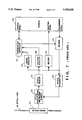
- FIG. 7 is a schematic block diagram of a communication interface unit of a terminal device employing the CSMA/CD method in the optical communication network (to be referred to as an optical CSMA/CD method hereinafter). The operation of the terminal will be described below with reference to FIG. 7.
- a terminal 39 connected to an optical fiber 10 via a optical coupler 21 and a communication interface transmits a signal to be transmitted onto the optical fiber 10, and sends it to another terminal on the network.
- a transmission operation based on the optical CSMA/CD method is performed in the following protocol.
- the terminal 39 which requests transmission outputs a control signal indicating a data transmission request to a communication controller 34.
- the communication controller 34 causes a carrier detector 25 to check if a signal from another terminal is transmitted onto the optical fiber 10. If it is detected that no signal from another terminal exists on the optical fiber 10, the communication controller 34 outputs, to the terminal 39, a control signal indicating that it is possible to start transmission.
- a transmission signal output from the terminal 39 in response to this control signal is encoded by an encoder 31, and the encoded signal is then converted into an optical signal by an optical transmitter 24.
- the optical signal is transmitted onto the optical fiber 10 via a demultiplexing/multiplexing element 22 and the optical coupler 21. In this case, the signal sent from the encoder 31 is input to the carrier detector 25, a collision detector 35 and a decoder 30 together with a signal received by an optical receiver 23, thereby the communication controller 34 monitors whether or not the transmission signal is normally transmitted.
- the present invention has been made to solve the above problems, and has its object to provide a reliable optical communication network, which can prevent erroneous detection of a transmission signal which is transmitted from its own terminal and reflected by a portion in a transmission path as a collision with a transmission signal from another terminal.
- Another object of the present invention is to provide an optical communication network having a collision detection function of transmitted optical signals which comprises detection means for detecting a reflection signal generated upon reflection of a transmission signal at an intermediate portion of a transmission path from a reception signal, and removing means for removing the reflection signal detected by the detection means from the reception signal.
- a Further object of the present invention is to provide an optical communication network connected through an optical transmission path, and having a collision detection function of transmitted optical signals which comprises reflection means for reflecting a transmission signal, and detection means for detecting a signal collision on the basis of the signal reflected by the reflection means
- FIG. 1 is a block diagram showing a communication interface according to the first embodiment of the present invention
- FIG. 2 is a schematic view showing an optical communication network of the first embodiment
- FIG. 3 is a block diagram showing a communication interface according to the second embodiment of the present invention.
- FIG. 4 is a block diagram showing a communication interface according to the third embodiment of the present invention.
- FIGS. 5(a) and 5(b) are schematic views showing light reflection portions in the third embodiment
- FIG. 6 is a block diagram showing a communication interface according to the fourth embodiment of the present invention.
- FIG. 7 is a block diagram for explaining a conventional optical CSMA/CD method.
- FIGS. 1 and 2 show an arrangement of the first embodiment of the present invention.
- FIG. 1 is a schematic block diagram showing an arrangement of a communication interface unit
- FIG. 2 is a schematic diagram showing a network arrangement using the unit shown in FIG. 1.
- reference numeral 10 denotes a transmission path using an optical fiber, which path constitutes a communication network.
- Reference numeral 21 denotes a optical coupler for sending some light components on the optical fiber 10 to a demultiplexing/multiplexing element 22, and sending light components from the demultiplexing/multiplexing element 22 onto the optical fiber 10.
- Reference numeral 23 denotes an optical receiver for converting optical signals into electrical signals.
- the optical receiver 23 includes a photodetector, an amplifier, and the like.
- Reference numeral 24 denotes an optical transmitter for converting electrical signals into optical signals.
- the optical transmitter 24 includes a semiconductor laser, a driver for the laser, and the like.
- Reference numeral 25 denotes a carrier detector for detecting whether or not a signal is transmitted onto the optical fiber 10.
- Reference numeral 26 denotes a local oscillator for generating a signal having a frequency almost equal to an input center frequency of a surface acoustic wave convolver 32 (to be described later).
- Reference numeral 27 denotes a time inverter for time-inverting a code string output from an encoder 31 (to be described later) in each unit time.
- Reference numerals 28 and 29 denote mixers.
- Reference numeral 30 denotes a decoder for decoding a code string converted by the optical receiver 23 into a normal signal.
- Reference numeral 31 denotes the encoder for encoding a signal to be transmitted into a code string suitable for transmission on the transmission path.
- Reference numeral 32 denotes the surface acoustic wave convolver for performing a convolution integral operation of input signals from the mixers 28 and 29.
- Reference numeral 33 denotes a detector.
- Reference numeral 34 denotes a communication controller for controlling transmission/reception with a terminal 39 (to be described later).
- Reference numeral 35 denotes a collision detector for detecting a collision of signals, and informing it to the communication controller 34.
- Reference numeral 36 denotes a subtracter for subtracting an output signal from the encoder 31 from an output signal from the optical receiver 23.
- Each of components 211 to 215 shown in FIG. 2 corresponds to the optical coupler 21 shown in FIG. 1, and each of components 411 to 415 corresponds to the terminal 39.
- Each of components 311 to 315 represents the overall arrangement excluding the optical fiber 10, the optical coupler 21, and the terminal 39 from the arrangement shown in FIG. 1, and will be referred to as a communication interface (I/F) hereinafter.
- I/F communication interface
- this embodiment employs a so-called bus-type network as a network pattern.
- Each terminal sends a signal onto the optical fiber 10 via the optical coupler using the communication I/F.
- Each terminal fetches some signal components on the optical fiber 10 via the optical coupler into the communication I/F, thereby receiving the signal.
- the terminal 39 When the terminal 39 transmits a signal according to a normal CSMA/CD protocol, it outputs a transmission request signal to the communication controller 34. In response to this signal, the communication controller 34 causes the carrier detector 25 to check whether or not a signal from another terminal is transmitted onto the optical fiber transmission path 10. As a result, if it is detected that no signal from another terminal is transmitted onto the optical fiber 10, the communication controller 34 outputs a signal for permitting transmission to the terminal 39. Upon reception of this signal, the terminal 39 causes the encoder 31 to convert a transmission signal into a code string suitable for a communication, and then causes the optical transmitter 24 to convert the code string into an optical signal. Thereafter, the terminal 39 transmits the optical signal onto the optical fiber 10 via the demultiplexing/multiplexing element 22 and the optical coupler 21.
- the output signal H(t) from the surface acoustic wave convolver 32 is input to the detector 33, and a component e j2wt is removed from the signal H(t).
- the output signal from the detector 33 is input to the amplitude/delay time detector 37.
- information indicating whether or not the same code string is included in both the signal input from the optical receiver 23 and the signal input from the encoder 31, and information indicating a delay amount of the code string if it is included are obtained from the output signal from the detector 33.
- this means that its own transmission signal reflected on the optical fiber transmission path 10 is received, and the presence/absence of a reflection signal and its delay time can be detected based on the output signal from the detector 33. Since the transmission signal and the reflection signal include a perfectly identical code string (F(t) G(t)), an attenuation amount of the reflection signal can also be detected based on the value of the coefficient k.
- the output signal from the encoder 31 is properly delayed and amplified (or attenuated) by the variable delay/amplifier circuit 38 in accordance with the information indicating the presence/absence of the reflection signal, the delay time of the reflection signal, and the attenuation amount obtained in this manner.
- the output signal from the delay/amplifier circuit 38 is subtracted from a reception signal input via the optical receiver 23 by the subtracter 36, thereby a reflection component of the transmission signal from its own terminal is removed from the reception signal, and only a Signal component from another terminal can be input to the collision detector 35.
- the communication controller 34 receives the output signal from the collision detector 3.5, and monitors whether or not a collision with a signal from another terminal occurs during transmission of a signal from its own terminal. When a collision occurs, the controller 34 informs this to the terminal 39, and sends a cancel signal indicating that the transmission signal is invalidated onto the optical fiber transmission path 10 via the encoder 31.
- a terminal which performs data transmission performs collision detection with always removing a reflection signal of a transmission signal output from its own terminal from a reception signal, a collision can be prevented from being erroneously detected due to the reflection signal.
- FIG. 3 is a schematic block diagram showing an arrangement of a communication interface unit of the second embodiment.
- the second embodiment can also be suitably used in an optical communication network shown in FIG. 2 like in the first embodiment.
- FIG. 3 denote blocks having the same functions as those in FIG. 1, and a description thereof will be omitted.
- a difference from the first embodiment is that the time inverter 27, the local oscillator 26, the surface acoustic wave convolver 32, and the mixers 28 and 29 are removed, and a waveshaper 40 and a sliding correlator 41 are added.
- a variable delay circuit 43 is used in this embodiment.
- a principal difference in operation between this embodiment and the first embodiment described above is as follows. That is, in the first embodiment, when a reflection signal of a signal transmitted from its own terminal is identified, a signal is processed as an analog amount. However, in this embodiment, the signal is processed as a digital amount.
- the operation of the second embodiment will be described below with reference to FIG. 3. Note that a protocol at the beginning of transmission is the same as that in the first embodiment.
- an optical signal received via the optical coupler 21 is transmitted to the optical receiver 23 via the demultiplexing/multiplexing element 22 and converted into an electrical signal by the optical receiver 23.
- the electrical signal is input to the waveshaper 40.
- the waveshaper 40 has a function of converting the input signal into a digital signal. More specifically, the optical receiver 23 outputs an electrical signal of a voltage proportional to the intensity of an input optical signal.
- the waveshaper 40 detects a threshold value of voltages corresponding to "0" and "1" from the output electrical signal, determines whether the input signal is "0" or "1" at each timing, and outputs a corresponding voltage.
- the output signal from the waveshaper 40 is input to one input terminal of the sliding correlator 41.
- the other input terminal of the correlator 41 receives an output signal from the encoder 31.
- the sliding correlator 41 is a kind of digital circuit, and compares two input code strings while sliding them along the time base, thereby obtaining a correlation between the two input code strings. More specifically, the sliding correlator 41 compares two code strings while shifting them along the time base, and when two code strings coincide with each other, the correlator 41 outputs a maximum signal.
- the correlator 41 whether or not the output signal from the waveshaper 40 and the output signal from the encoder 31 include the same code string, i.e., whether or not an input signal from the optical transmission path 10 includes a reflection signal component, can be detected. If the reflection signal component is included, a delay amount of the reflection signal from an original signal can also be detected.
- the output signal from the encoder 31 is delayed by a time corresponding to the detected delay time by the variable delay circuit 43.
- the subtracter 36 subtracts the output signal from the delay circuit 43 from the output signal from the waveshaper 40. In this manner, a reflection signal component of a transmission signal from its own terminal can be removed from a reception signal.
- this signal is input to the collision detector 35 and collision detection is performed.
- the protocol after the collision is detected is the same as that in the first embodiment.
- the first embodiment employs a surface acoustic wave convolver 32, processing for identifying a reflection signal component of a transmission signal from its own terminal can be performed at high speed, and the first embodiment is suitable for high-speed data transmission.
- the first embodiment requires a local oscillator 26, a time inverter 27, and the like, a system becomes relatively expensive.
- the second embodiment employs a sliding correlator 41, and performs identification processing of a reflection signal in a digital manner, a relatively inexpensive system can be realized although the second embodiment may not be applied to high-speed transmission.
- a surface acoustic wave convolver or a sliding correlator is used to perform a convolution integral operation or a correlation operation of signals.
- a CCD correlator may be used as long as it can provide the same function as that of the convolver or the correlator.
- FIG. 4 shows the third embodiment of the present invention.
- FIG. 4 is a schematic block diagram showing an arrangement of a node of a network, and a network has the same arrangement as that shown in FIG. 2.
- reference numeral 10 denotes an optical fiber as a transmission path, which constitutes a communication network.
- Reference numeral 21 denotes a optical coupler for sending some light components on the optical fiber 10 to a demultiplexing/multiplexing element 22, and sending light components from the demultiplexing/multiplexing element 22 onto the optical fiber 10.
- Reference numeral 23 denotes an optical receiver for converting optical signals into electrical signals.
- the optical receiver 23 includes a photodetector, an amplifier, and the like.
- Reference numeral 24 denotes an optical transmitter for converting electrical signals into optical signals.
- the optical transmitter 24 includes a light source such as a semiconductor laser, a driver for the laser, and the like.
- Reference numeral 50 denotes a light reflector for reflecting some components of an optical signal sent from the optical transmitter 24, and returning the reflected light components to the optical receiver 23.
- This embodiment also employs a so-called bus-type optical network as a network pattern.
- Each terminal sends a signal onto the optical fiber 10 via the optical coupler 21 using the communication I/F, or causes the optical coupler 21 to fetch some components of signals on the transmission path 10 into the communication I/F, thereby receiving signals.
- the terminal 39 monitors the transmission signal using the optical signal reflected by the light reflector 50.
- the terminal 39 transmits a signal
- two cases must be identified. More specifically, as described above, one case is that another terminal has started transmission at almost the same time due to a transmission delay of a signal on the optical fiber 10. Another case is that the transmission signal from its own terminal, which signal is reflected by a reflection surface on the optical fiber transmission path 10 is transmitted to the optical receiver 23 of its own node via the optical coupler 21.
- an optical signal from another terminal, and a transmission optical signal from its own terminal, which signal is partially reflected by the light reflector 50, are input on the optical receiver 23, and a signal collision is detected by the collision detector 35. After an elapse of a predetermined period of time, the normal CSMA/CD re-transmission protocol is executed.
- the reflectance of the light reflector 50 is set so that, of optical signal components transmitted from the optical transmitter 24, the amount of light components reflected by the light reflector 50 and incident on the optical receiver 23 is sufficiently larger than the amount of light components reflected on the optical fiber transmission path 10, and returned to the optical receiver 23.
- the minimum light-receiving sensitivity of the optical receiver 23 is set to be an intermediate value between the amount of light components reflected by the light reflector 50 and the amount of light components reflected by the reflection surface on the optical fiber transmission path 10
- the optical receiver 23 can detect only the optical signal components reflected by the light reflector 50, and interference caused by the optical signal components reflected by the reflection surface on the optical fiber transmission path 10 can be eliminated, thus avoiding erroneous detection of a signal collision.
- the reflectance of the light reflector 50 can be selected in correspondence with the arrangement of the optical communication network according to the above-mentioned setting method.
- FIGS. 5(a) and 5(b) are schematic views showing the light reflector 50 of this embodiment.
- a partial reflection film 112 for reflecting some components of incident light is arranged midway along the optical fiber 110.
- an optical demultiplexing/multiplexing device 114 prepared by, e.g., welding using an optical fiber is utilized.
- the terminal end of one optical fiber 111 connected to the optical coupler 21 serves as a reflection end 113.
- the reflectance of each of the partial reflection film 112 and the reflection end 113 can be set so that reflection light having a sufficiently larger light amount than that of return light from the optical fiber transmission path as an error signal can be returned to the optical receiver 23, thereby preventing erroneous detection of a signal collision.
- the light reflector shown in FIG. 5(b) utilizes the optical demultiplexing/multiplexing device 114.
- the optical demultiplexing/multiplexing device 114 may be used as the optical demultiplexing/multiplexing element 22 shown in FIG. 4.
- the light reflector 50 may be arranged in the optical demultiplexing/multiplexing element 22 as long as it has the above-mentioned function.
- the reflector 50 may be arranged in the optical coupler 21.
- FIG. 6 is a schematic block diagram showing an arrangement of a node of this embodiment. This embodiment can also be suitably used in the optical communication network shown in FIG. 2 like in the first embodiment.
- FIG. 6 denote blocks having the same functions as in FIG. 4, and a detailed description thereof will be omitted.
- a difference from FIG. 4 is that an optical attenuator 51 for decreasing the light amount of passing light is added between the optical coupler 21 and the light reflector 50.
- the transmission and reception protocols of this embodiment are the same as those in the third embodiment.
- a difference from the third embodiment is as follows. Since the optical attenuator 51 is added, the light amount of an optical signal incident from another node to the optical receiver 23 is decreased by an attenuation amount defined by the optical attenuator 51, and the light amount of an optical signal returned to the optical receiver 23 upon reflection on the optical fiber transmission path 10 is decreased by the attenuation amount defined when the signal reciprocates through the optical attenuator 51.
- the difference between the light amount of a return signal incident from the light reflector 50 to the optical receiver 23 and the light amount of a return signal from the reflection surface on the optical fiber transmission path 10 is increased as compared to the third embodiment.
- the minimum light-receiving sensitivity of the optical receiver 23 is set to be an intermediate value between the two light amounts, interference caused by the return signal from the reflection surface on the optical fiber transmission path 10 can be eliminated, and erroneous detection of a signal collision can be avoided.
- At least one optical attenuator 51 need only be arranged between the optical fiber transmission path 10 and the light reflector 50, and may be included in the optical coupler 21.
- the light amount of a signal returned from the reflection surface on the optical fiber transmission path 10 to the optical receiver 23 can be decreased more than that in the third embodiment, performance in preventing erroneous detection of a signal collision can be improved.
- the number of the light reflectors 50 is not limited to one.
- a plurality of light reflectors 50 may be arranged as long as erroneous detection of a monitor signal and a signal collision can be prevented.
- the description has been made using a normal bus-type optical communication network as an example.
- the present invention can be applied to any other optical communication networks, such as a bus-type optical communication network in which an optical amplifier is arranged on a communication path, or a non-bus type network, e.g., a star-type optical communication network, or a loop-type optical communication network, as long as a transmission signal from its own node is returned to the optical receiver 23, and causes erroneous detection of a signal collision.
- the present invention can be applied to an optical communication network which is multiplexed using, e.g., a waveform multiplexing method if a system requires collision detection of signals on a transmission path.
Priority Applications (1)
| Application Number | Priority Date | Filing Date | Title |
|---|---|---|---|
| US08/243,528 US5390039A (en) | 1990-08-27 | 1994-05-16 | Optical network for detecting collisions based on the reflection of a transmitting signal |
Applications Claiming Priority (7)
| Application Number | Priority Date | Filing Date | Title |
|---|---|---|---|
| JP2-222515 | 1990-08-27 | ||
| JP2222515A JP2817116B2 (ja) | 1990-08-27 | 1990-08-27 | 通信インターフェース装置及び光通信ネットワーク |
| JP2222514A JP2817115B2 (ja) | 1990-08-27 | 1990-08-27 | 通信インターフェース装置及び光通信ネットワーク |
| JP2-222514 | 1990-08-27 | ||
| US74881191A | 1991-08-22 | 1991-08-22 | |
| US8058593A | 1993-06-24 | 1993-06-24 | |
| US08/243,528 US5390039A (en) | 1990-08-27 | 1994-05-16 | Optical network for detecting collisions based on the reflection of a transmitting signal |
Related Parent Applications (1)
| Application Number | Title | Priority Date | Filing Date |
|---|---|---|---|
| US8058593A Continuation | 1990-08-27 | 1993-06-24 |
Publications (1)
| Publication Number | Publication Date |
|---|---|
| US5390039A true US5390039A (en) | 1995-02-14 |
Family
ID=26524923
Family Applications (1)
| Application Number | Title | Priority Date | Filing Date |
|---|---|---|---|
| US08/243,528 Expired - Fee Related US5390039A (en) | 1990-08-27 | 1994-05-16 | Optical network for detecting collisions based on the reflection of a transmitting signal |
Country Status (4)
| Country | Link |
|---|---|
| US (1) | US5390039A (de) |
| EP (1) | EP0473100B1 (de) |
| AT (1) | ATE130145T1 (de) |
| DE (1) | DE69114414T2 (de) |
Cited By (6)
| Publication number | Priority date | Publication date | Assignee | Title |
|---|---|---|---|---|
| WO1996020462A1 (en) * | 1994-12-28 | 1996-07-04 | Motorola Inc. | Method, transceiver, and system for providing wireless communication compatible with 10base-t ethernet |
| US5586054A (en) * | 1994-07-08 | 1996-12-17 | Fluke Corporation | time-domain reflectometer for testing coaxial cables |
| US5903369A (en) * | 1996-07-03 | 1999-05-11 | Ltel Corporation | Optical wireless communication method and apparatus |
| US6848010B1 (en) * | 2000-03-31 | 2005-01-25 | Intel Corporation | Data collision detection in networks |
| US20050089326A1 (en) * | 2003-10-03 | 2005-04-28 | Zvi Regev | Cancellation of transmitted signal crosstalk in optical receivers of diplexer-based fiber optic transceivers |
| US20110008045A1 (en) * | 2009-07-09 | 2011-01-13 | Alcatel-Lucent Usa, Inc. | Detecting collisions on multipoint shared optical media |
Families Citing this family (1)
| Publication number | Priority date | Publication date | Assignee | Title |
|---|---|---|---|---|
| DE10106699C2 (de) * | 2001-02-14 | 2003-11-27 | Leica Microsystems | Berührungssensor und Vorrichtung zum Schutz eines hervorstehenden Bauteils |
Citations (13)
| Publication number | Priority date | Publication date | Assignee | Title |
|---|---|---|---|---|
| US3928805A (en) * | 1973-09-20 | 1975-12-23 | Marconi Co Canada | Detectability of emergency beacon |
| JPS5662436A (en) * | 1979-10-29 | 1981-05-28 | Nec Corp | Optical multiplex transmission system |
| JPS5687946A (en) * | 1979-12-20 | 1981-07-17 | Fujitsu Ltd | Optical fiber communication equipment |
| JPS58132674A (ja) * | 1982-02-03 | 1983-08-08 | Nippon Telegr & Teleph Corp <Ntt> | 伝送線路障害探索法 |
| JPS58204644A (ja) * | 1982-05-24 | 1983-11-29 | Toshiba Corp | 光ネットワ−ク監視装置 |
| US4516221A (en) * | 1981-06-26 | 1985-05-07 | Hitachi, Ltd. | Data communication system |
| DD224730A1 (de) * | 1984-06-12 | 1985-07-10 | Ilmenau Tech Hochschule | Anordnung zur darstellung der faltungsoperation |
| US4723311A (en) * | 1982-12-14 | 1988-02-02 | Siemens Aktiengesellschaft | Method and apparatus for recognizing data collisions in an optical data bus |
| US4751701A (en) * | 1985-11-14 | 1988-06-14 | Hughes Network Systems, Inc. | TDM collision detector |
| US4809361A (en) * | 1985-11-13 | 1989-02-28 | Fujitsu Limited | Optical composite transceiver |
| US4815802A (en) * | 1984-12-03 | 1989-03-28 | Canon Kabushiki Kaisha | Surface acoustic wave generating apparatus including a positive feedback-type generator |
| US4975926A (en) * | 1989-03-30 | 1990-12-04 | Guenther Knapp | Wireless indoor data communication system |
| US5005212A (en) * | 1989-12-12 | 1991-04-02 | At&T Bell Laboratories | Interference suppression in optical communication systems |
-
1991
- 1991-08-26 AT AT91114303T patent/ATE130145T1/de not_active IP Right Cessation
- 1991-08-26 DE DE69114414T patent/DE69114414T2/de not_active Expired - Fee Related
- 1991-08-26 EP EP91114303A patent/EP0473100B1/de not_active Expired - Lifetime
-
1994
- 1994-05-16 US US08/243,528 patent/US5390039A/en not_active Expired - Fee Related
Patent Citations (13)
| Publication number | Priority date | Publication date | Assignee | Title |
|---|---|---|---|---|
| US3928805A (en) * | 1973-09-20 | 1975-12-23 | Marconi Co Canada | Detectability of emergency beacon |
| JPS5662436A (en) * | 1979-10-29 | 1981-05-28 | Nec Corp | Optical multiplex transmission system |
| JPS5687946A (en) * | 1979-12-20 | 1981-07-17 | Fujitsu Ltd | Optical fiber communication equipment |
| US4516221A (en) * | 1981-06-26 | 1985-05-07 | Hitachi, Ltd. | Data communication system |
| JPS58132674A (ja) * | 1982-02-03 | 1983-08-08 | Nippon Telegr & Teleph Corp <Ntt> | 伝送線路障害探索法 |
| JPS58204644A (ja) * | 1982-05-24 | 1983-11-29 | Toshiba Corp | 光ネットワ−ク監視装置 |
| US4723311A (en) * | 1982-12-14 | 1988-02-02 | Siemens Aktiengesellschaft | Method and apparatus for recognizing data collisions in an optical data bus |
| DD224730A1 (de) * | 1984-06-12 | 1985-07-10 | Ilmenau Tech Hochschule | Anordnung zur darstellung der faltungsoperation |
| US4815802A (en) * | 1984-12-03 | 1989-03-28 | Canon Kabushiki Kaisha | Surface acoustic wave generating apparatus including a positive feedback-type generator |
| US4809361A (en) * | 1985-11-13 | 1989-02-28 | Fujitsu Limited | Optical composite transceiver |
| US4751701A (en) * | 1985-11-14 | 1988-06-14 | Hughes Network Systems, Inc. | TDM collision detector |
| US4975926A (en) * | 1989-03-30 | 1990-12-04 | Guenther Knapp | Wireless indoor data communication system |
| US5005212A (en) * | 1989-12-12 | 1991-04-02 | At&T Bell Laboratories | Interference suppression in optical communication systems |
Non-Patent Citations (2)
| Title |
|---|
| "Services Integration and Multiplexing for Broad-Band Communication Systems", I.E.E.E. Journal on Selected Areas in Communications, vol. SAC-4, No. 4, Jul. 1986, pp. 551-564. |
| Services Integration and Multiplexing for Broad Band Communication Systems , I.E.E.E. Journal on Selected Areas in Communications, vol. SAC 4, No. 4, Jul. 1986, pp. 551 564. * |
Cited By (9)
| Publication number | Priority date | Publication date | Assignee | Title |
|---|---|---|---|---|
| US5586054A (en) * | 1994-07-08 | 1996-12-17 | Fluke Corporation | time-domain reflectometer for testing coaxial cables |
| WO1996020462A1 (en) * | 1994-12-28 | 1996-07-04 | Motorola Inc. | Method, transceiver, and system for providing wireless communication compatible with 10base-t ethernet |
| US5636213A (en) * | 1994-12-28 | 1997-06-03 | Motorola | Method, transceiver, and system for providing wireless communication compatible with 10BASE-T Ethernet |
| AU681053B2 (en) * | 1994-12-28 | 1997-08-14 | Google Technology Holdings LLC | Method, transceiver, and system for providing wireless communication compatible with 10base-T ethernet |
| US5903369A (en) * | 1996-07-03 | 1999-05-11 | Ltel Corporation | Optical wireless communication method and apparatus |
| US6848010B1 (en) * | 2000-03-31 | 2005-01-25 | Intel Corporation | Data collision detection in networks |
| US20050089326A1 (en) * | 2003-10-03 | 2005-04-28 | Zvi Regev | Cancellation of transmitted signal crosstalk in optical receivers of diplexer-based fiber optic transceivers |
| US20110008045A1 (en) * | 2009-07-09 | 2011-01-13 | Alcatel-Lucent Usa, Inc. | Detecting collisions on multipoint shared optical media |
| US8290368B2 (en) * | 2009-07-09 | 2012-10-16 | Alcatel Lucent | Detecting collisions on multipoint shared optical media |
Also Published As
| Publication number | Publication date |
|---|---|
| ATE130145T1 (de) | 1995-11-15 |
| DE69114414D1 (de) | 1995-12-14 |
| DE69114414T2 (de) | 1996-04-18 |
| EP0473100A1 (de) | 1992-03-04 |
| EP0473100B1 (de) | 1995-11-08 |
Similar Documents
| Publication | Publication Date | Title |
|---|---|---|
| JP3701979B2 (ja) | ワイヤレス・キャリア・センス多元接続システムにおいて、衝突検出を行う方法,装置,ワイヤレス送受信機およびコンピュータ | |
| US5631757A (en) | Full-duplex data communication system using different transmit and receive data symbol lengths | |
| GB2292495A (en) | Fault location in optical communications systems | |
| JPH11509067A (ja) | 光伝送システムにおける自己刺激信号の検出 | |
| JPH06268598A (ja) | 光通信監視システムおよび方法 | |
| US5390039A (en) | Optical network for detecting collisions based on the reflection of a transmitting signal | |
| EP1701186A1 (de) | Elektrooptischer Verzögerungsleitungs-diskriminator | |
| JPH11136188A (ja) | 光ファイバーネットワーク上の光伝送のための方法、及び光通信ネットワーク | |
| JP3529263B2 (ja) | 空間伝送用光送受信回路および空間伝送装置 | |
| EP0840963B1 (de) | Verfahren und einrichtung zur abstandmessung in einem tdma-system, eines passiven optischen netzes | |
| US4998295A (en) | Receiver having an interferometer | |
| JP2817115B2 (ja) | 通信インターフェース装置及び光通信ネットワーク | |
| JP2817116B2 (ja) | 通信インターフェース装置及び光通信ネットワーク | |
| RU2115245C1 (ru) | Способ контроля оптических широкополосных соединительных линий вплоть до пассивного стыка | |
| JPH0650841A (ja) | 光ファイバ線路破断検出方法およびその装置 | |
| JP2616480B2 (ja) | バースト光受信回路 | |
| JP2546171B2 (ja) | 反射光消去形光送受信回路 | |
| JP4069036B2 (ja) | マーク率評価装置 | |
| JP2601778B2 (ja) | 光スイッチの同期切替通信方法 | |
| JPH104386A (ja) | 光ホモダイン検波通信方式及び装置とこれを用いた光符号分割多重伝送方式及び装置 | |
| JP3176947B2 (ja) | 光ケーブル切断検出方法 | |
| JPH0568152U (ja) | 光信号受信装置 | |
| JPH06350531A (ja) | 光入力断検出方法及び光入力断検出装置 | |
| JPH06132892A (ja) | データ転送方式 | |
| JPH05327620A (ja) | 光線路断検出装置 |
Legal Events
| Date | Code | Title | Description |
|---|---|---|---|
| CC | Certificate of correction | ||
| FPAY | Fee payment |
Year of fee payment: 4 |
|
| FEPP | Fee payment procedure |
Free format text: PAYOR NUMBER ASSIGNED (ORIGINAL EVENT CODE: ASPN); ENTITY STATUS OF PATENT OWNER: LARGE ENTITY Free format text: PAYER NUMBER DE-ASSIGNED (ORIGINAL EVENT CODE: RMPN); ENTITY STATUS OF PATENT OWNER: LARGE ENTITY |
|
| FPAY | Fee payment |
Year of fee payment: 8 |
|
| REMI | Maintenance fee reminder mailed | ||
| LAPS | Lapse for failure to pay maintenance fees | ||
| STCH | Information on status: patent discontinuation |
Free format text: PATENT EXPIRED DUE TO NONPAYMENT OF MAINTENANCE FEES UNDER 37 CFR 1.362 |
|
| FP | Lapsed due to failure to pay maintenance fee |
Effective date: 20070214 |