US5374587A - Method of manufacturing optical semiconductor element - Google Patents
Method of manufacturing optical semiconductor element Download PDFInfo
- Publication number
- US5374587A US5374587A US07/920,880 US92088092A US5374587A US 5374587 A US5374587 A US 5374587A US 92088092 A US92088092 A US 92088092A US 5374587 A US5374587 A US 5374587A
- Authority
- US
- United States
- Prior art keywords
- active layer
- amplifier
- semiconductor
- ridge
- mask
- Prior art date
- Legal status (The legal status is an assumption and is not a legal conclusion. Google has not performed a legal analysis and makes no representation as to the accuracy of the status listed.)
- Expired - Fee Related
Links
Images


Classifications
-
- H—ELECTRICITY
- H10—SEMICONDUCTOR DEVICES; ELECTRIC SOLID-STATE DEVICES NOT OTHERWISE PROVIDED FOR
- H10H—INORGANIC LIGHT-EMITTING SEMICONDUCTOR DEVICES HAVING POTENTIAL BARRIERS
- H10H20/00—Individual inorganic light-emitting semiconductor devices having potential barriers, e.g. light-emitting diodes [LED]
- H10H20/80—Constructional details
- H10H20/84—Coatings, e.g. passivation layers or antireflective coatings
-
- H—ELECTRICITY
- H01—ELECTRIC ELEMENTS
- H01S—DEVICES USING THE PROCESS OF LIGHT AMPLIFICATION BY STIMULATED EMISSION OF RADIATION [LASER] TO AMPLIFY OR GENERATE LIGHT; DEVICES USING STIMULATED EMISSION OF ELECTROMAGNETIC RADIATION IN WAVE RANGES OTHER THAN OPTICAL
- H01S5/00—Semiconductor lasers
- H01S5/20—Structure or shape of the semiconductor body to guide the optical wave ; Confining structures perpendicular to the optical axis, e.g. index or gain guiding, stripe geometry, broad area lasers, gain tailoring, transverse or lateral reflectors, special cladding structures, MQW barrier reflection layers
- H01S5/22—Structure or shape of the semiconductor body to guide the optical wave ; Confining structures perpendicular to the optical axis, e.g. index or gain guiding, stripe geometry, broad area lasers, gain tailoring, transverse or lateral reflectors, special cladding structures, MQW barrier reflection layers having a ridge or stripe structure
- H01S5/227—Buried mesa structure ; Striped active layer
-
- H—ELECTRICITY
- H10—SEMICONDUCTOR DEVICES; ELECTRIC SOLID-STATE DEVICES NOT OTHERWISE PROVIDED FOR
- H10H—INORGANIC LIGHT-EMITTING SEMICONDUCTOR DEVICES HAVING POTENTIAL BARRIERS
- H10H20/00—Individual inorganic light-emitting semiconductor devices having potential barriers, e.g. light-emitting diodes [LED]
- H10H20/01—Manufacture or treatment
- H10H20/011—Manufacture or treatment of bodies, e.g. forming semiconductor layers
- H10H20/013—Manufacture or treatment of bodies, e.g. forming semiconductor layers having light-emitting regions comprising only Group III-V materials
-
- H—ELECTRICITY
- H10—SEMICONDUCTOR DEVICES; ELECTRIC SOLID-STATE DEVICES NOT OTHERWISE PROVIDED FOR
- H10P—GENERIC PROCESSES OR APPARATUS FOR THE MANUFACTURE OR TREATMENT OF DEVICES COVERED BY CLASS H10
- H10P14/00—Formation of materials, e.g. in the shape of layers or pillars
- H10P14/20—Formation of materials, e.g. in the shape of layers or pillars of semiconductor materials
- H10P14/24—Formation of materials, e.g. in the shape of layers or pillars of semiconductor materials using chemical vapour deposition [CVD]
-
- H—ELECTRICITY
- H10—SEMICONDUCTOR DEVICES; ELECTRIC SOLID-STATE DEVICES NOT OTHERWISE PROVIDED FOR
- H10P—GENERIC PROCESSES OR APPARATUS FOR THE MANUFACTURE OR TREATMENT OF DEVICES COVERED BY CLASS H10
- H10P14/00—Formation of materials, e.g. in the shape of layers or pillars
- H10P14/20—Formation of materials, e.g. in the shape of layers or pillars of semiconductor materials
- H10P14/27—Formation of materials, e.g. in the shape of layers or pillars of semiconductor materials using selective deposition, e.g. simultaneous growth of monocrystalline and non-monocrystalline semiconductor materials
- H10P14/271—Formation of materials, e.g. in the shape of layers or pillars of semiconductor materials using selective deposition, e.g. simultaneous growth of monocrystalline and non-monocrystalline semiconductor materials characterised by the preparation of substrate for selective deposition
-
- H—ELECTRICITY
- H10—SEMICONDUCTOR DEVICES; ELECTRIC SOLID-STATE DEVICES NOT OTHERWISE PROVIDED FOR
- H10P—GENERIC PROCESSES OR APPARATUS FOR THE MANUFACTURE OR TREATMENT OF DEVICES COVERED BY CLASS H10
- H10P14/00—Formation of materials, e.g. in the shape of layers or pillars
- H10P14/20—Formation of materials, e.g. in the shape of layers or pillars of semiconductor materials
- H10P14/29—Formation of materials, e.g. in the shape of layers or pillars of semiconductor materials characterised by the substrates
- H10P14/2901—Materials
- H10P14/2907—Materials being Group IIIA-VA materials
- H10P14/2909—Phosphides
-
- H—ELECTRICITY
- H10—SEMICONDUCTOR DEVICES; ELECTRIC SOLID-STATE DEVICES NOT OTHERWISE PROVIDED FOR
- H10P—GENERIC PROCESSES OR APPARATUS FOR THE MANUFACTURE OR TREATMENT OF DEVICES COVERED BY CLASS H10
- H10P14/00—Formation of materials, e.g. in the shape of layers or pillars
- H10P14/20—Formation of materials, e.g. in the shape of layers or pillars of semiconductor materials
- H10P14/34—Deposited materials, e.g. layers
- H10P14/3402—Deposited materials, e.g. layers characterised by the chemical composition
- H10P14/3414—Deposited materials, e.g. layers characterised by the chemical composition being group IIIA-VIA materials
- H10P14/3418—Phosphides
-
- H—ELECTRICITY
- H10—SEMICONDUCTOR DEVICES; ELECTRIC SOLID-STATE DEVICES NOT OTHERWISE PROVIDED FOR
- H10P—GENERIC PROCESSES OR APPARATUS FOR THE MANUFACTURE OR TREATMENT OF DEVICES COVERED BY CLASS H10
- H10P14/00—Formation of materials, e.g. in the shape of layers or pillars
- H10P14/20—Formation of materials, e.g. in the shape of layers or pillars of semiconductor materials
- H10P14/34—Deposited materials, e.g. layers
- H10P14/3402—Deposited materials, e.g. layers characterised by the chemical composition
- H10P14/3414—Deposited materials, e.g. layers characterised by the chemical composition being group IIIA-VIA materials
- H10P14/3421—Arsenides
-
- H—ELECTRICITY
- H01—ELECTRIC ELEMENTS
- H01S—DEVICES USING THE PROCESS OF LIGHT AMPLIFICATION BY STIMULATED EMISSION OF RADIATION [LASER] TO AMPLIFY OR GENERATE LIGHT; DEVICES USING STIMULATED EMISSION OF ELECTROMAGNETIC RADIATION IN WAVE RANGES OTHER THAN OPTICAL
- H01S5/00—Semiconductor lasers
- H01S5/20—Structure or shape of the semiconductor body to guide the optical wave ; Confining structures perpendicular to the optical axis, e.g. index or gain guiding, stripe geometry, broad area lasers, gain tailoring, transverse or lateral reflectors, special cladding structures, MQW barrier reflection layers
- H01S5/22—Structure or shape of the semiconductor body to guide the optical wave ; Confining structures perpendicular to the optical axis, e.g. index or gain guiding, stripe geometry, broad area lasers, gain tailoring, transverse or lateral reflectors, special cladding structures, MQW barrier reflection layers having a ridge or stripe structure
- H01S5/227—Buried mesa structure ; Striped active layer
- H01S5/2272—Buried mesa structure ; Striped active layer grown by a mask induced selective growth
-
- H—ELECTRICITY
- H01—ELECTRIC ELEMENTS
- H01S—DEVICES USING THE PROCESS OF LIGHT AMPLIFICATION BY STIMULATED EMISSION OF RADIATION [LASER] TO AMPLIFY OR GENERATE LIGHT; DEVICES USING STIMULATED EMISSION OF ELECTROMAGNETIC RADIATION IN WAVE RANGES OTHER THAN OPTICAL
- H01S5/00—Semiconductor lasers
- H01S5/50—Amplifier structures not provided for in groups H01S5/02 - H01S5/30
- H01S5/5036—Amplifier structures not provided for in groups H01S5/02 - H01S5/30 the arrangement being polarisation-selective
-
- Y—GENERAL TAGGING OF NEW TECHNOLOGICAL DEVELOPMENTS; GENERAL TAGGING OF CROSS-SECTIONAL TECHNOLOGIES SPANNING OVER SEVERAL SECTIONS OF THE IPC; TECHNICAL SUBJECTS COVERED BY FORMER USPC CROSS-REFERENCE ART COLLECTIONS [XRACs] AND DIGESTS
- Y10—TECHNICAL SUBJECTS COVERED BY FORMER USPC
- Y10S—TECHNICAL SUBJECTS COVERED BY FORMER USPC CROSS-REFERENCE ART COLLECTIONS [XRACs] AND DIGESTS
- Y10S148/00—Metal treatment
- Y10S148/026—Deposition thru hole in mask
Definitions
- the present invention relates to a method of manufacturing an optical semiconductor element and, more particularly, to a method of manufacturing an optical semiconductor element having an epitaxially grown ridge.
- an optical amplifier As an optical amplifier, a rare-earth (Er, Nd, or the like) added optical fiber amplifier, and a semiconductor laser amplifier (to be abbreviated to as an LD amplifier hereinafter) are expected to be useful in optical communications.
- an LD amplifier especially has compactness so that it should be appropriate to compact integrated components, and can cope with any wavelengths for optical communications.
- the polarization dependency of the gain in the LD amplifier is eliminated by adopting a strained quantum well structure (reference 1), a buried double-hetero structure having an active layer with a small width (up to 4,000 ⁇ or less) (reference 2), or a structure having a thick active layer (reference 4).
- reference 1 a strained quantum well structure
- reference 2 a buried double-hetero structure having an active layer with a small width (up to 4,000 ⁇ or less)
- reference 4 a structure having a thick active layer
- the LD amplifier having the narrow active layer of the reference 2 has a difficulty in its manufacturing process, and it is difficult to form this LD amplifier with good reproducibility.
- a compound semiconductor including the active layer is incised into a narrow (4,000- ⁇ wide) mesa-stripe shape. It is very difficult to realize this incision process by a conventional wet etching process with good reproducibility.
- the ripple of the gain must be considered.
- the ripple is caused by reflection of signal light propagating through a waveguide in the amplifier on the facet of an LD amplifier element.
- an optical semiconductor element including at least the steps of forming a mask having a stripe-like gap or interval on a semiconductor substrate, epitaxially growing a semiconductor ridge including an active layer only on gap or interval portion of the semiconductor substrate, and epitaxially growing a semiconductor cladding layer to cover the ridge, wherein a width of the active layer is less than 5,000 ⁇ .
- the polarization dependency of the gain of an LD amplifier having a bulk active layer is caused by the fact that the ratio of light (propagating wave) confined in a region where optical amplification is performed (active layer) (i.e., optical confinement ratio) has a polarization dependency.
- active layer i.e., optical confinement ratio
- TE light has a confinement ratio in the stacking direction which is larger than the confinement ratio of TM light.
- the optical confinement ratio is associated with the ratio of light leaking and propagating outside the active layer. The larger ratio of such leaking light is larger for the TM light than it is for the light.
- the leaking ratio of TM light is smaller than that of TE light, and this fact compensates for a small optical confinement ratio of TM light in the stacking direction.
- the optical confinement ratio of TE light is higher than that of TM light. For this reason, the gain of TE light is larger than that of TM light.
- the width of the active layer should be decreased to be as small as about 5,000 ⁇ , so that the sectional shape of the active layer approaches to a symmetrical sectional shape, thereby decreasing the polarization dependency of the optical confinement ratio in the active layer.
- the active layer having the above-mentioned sectional shape can be formed without posing a problem in its manufacturing process.
- a ridge having an active layer can be epitaxially grown on a semiconductor substrate, so that the ridge width is decreased toward the upper portion of the ridge.
- the ridge is epitaxially grown on an exposed (100) surface between the masks which have a stripe-like gap or interval in a (011) direction.
- the ridge has (111) side surfaces and is formed at 55° direction.
- the ripples of the gain are caused by reflection of a propagating wave on the facet of the LD amplifier.
- it is effective to form a window structure where the active layer as a waveguide disappears.
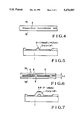
- FIG. 1 is a sectional view showing a ridge formed in an epitaxial growth process according to the present invention
- FIG. 2 is a perspective view showing an LD amplifier manufactured by a method according to an embodiment of the present invention
- FIG. 3 is a sectional view of the LD amplifier taken along a plane including a line A-A' in FIG. 2, and perpendicular to a substrate;
- FIG. 4 is a top view of a substrate formed with a mask according to the embodiment shown in FIG. 2;
- FIG. 5 is a sectional view, taken along a position V-V' in FIG. 4, of the substrate formed with a ridge according to the embodiment shown in FIG. 1;
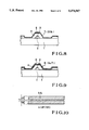
- FIG. 6 is a top view of the substrate when an inner portion of the mask is etched
- FIG. 7 is a sectional view of the substrate when another epitaxial growth is performed on the substrate shown in FIG. 6;
- FIG. 8 is a sectional view of the substrate obtained by forming an insulating film 7 on the structure shown in FIG. 7;
- FIG. 9 is a sectional view of the substrate obtained when the insulating layer 7 is removed on the upper surface of a capping layer 6, and an electrode 8 is formed;
- FIG. 10 is a top view of a substrate formed with a mask according to another embodiment of a method of the present invention adopting a structure having no window structure.
- FIG. 2 shows an LD amplifier manufactured by a method according to an embodiment of the present invention.
- FIG. 3 shows the sectional structure of the LD amplifier cut along a plane parallel to a line A-A' in FIG. 2 and perpendicular to the surface of a substrate 1. This LD amplifier is manufactured in the following procedure.
- a mask of a 21.5- ⁇ m wide stripe-like SiO 2 thin film having a gap portion with a width of 1.5 ⁇ m and a length of 300 ⁇ m is formed on the surface (100 surface) of an n-type InP substrate 1 (FIG. 4).
- the stripe-like SiO 2 thin film is formed by a thermal CVD method at a temperature of 375° C. using an (SiO 2 +O 2 ) normal pressure gas as a source gas. At this time, the thickness of the SiO 2 thin film is about 1,000 ⁇ .
- the mask is formed via a conventional resist process and an SiO 2 etching process by a dilute hydrogen fluoride solution treatment. This method is known to those who are skilled in the art.
- Epitaxial growth is selectively performed on the gap portion from which the surface of the substrate is exposed, thereby forming a ridge including an n-type cladding layer 2 and an i-type active layer 3.
- the active layer 3 has a thickness of 2,000 ⁇ , and a width of 4,000 ⁇ (FIG. 5).
- This epitaxial growth implies the following phenomenon. That is, when the substrate is heated in a source gas atmosphere with semiconductor composition, the source gas is decomposed, and the components of the semiconductor are deposited. With this epitaxial growth, a semiconductor layer having a pyramid-like section is formed, as shown in FIG. 5. Layers formed on the outer sides of the mask are those which are inevitably formed when a ridge is epitaxially grown, and which have no influence to the functions of the LD amplifier.
- a p-type p + -type/InP InGaAs layer is epitaxially grown on the gap portion widened to 6.5 ⁇ m so as to cover the ridge, thereby simultaneously forming a p-type cladding layer 4 and a window structure 5. Furthermore, a p + -type capping layer 6 is formed. This state is shown in FIG. 7.
- the window structure 5 is named after a structure in which when the p-type cladding layer 4 is deposited on a portion between the two ridge ends, no i-type active layer 3 is present on this portion.
- an LD amplifier is finally incised from the substrate, the substrate is cleaved at the central line of this window structure portion.
- the window portion is present at the end of the LD amplifier, and a facet where the active layer disappears at this end portion is also called a window facet.
- This window structure can provide an effect for decreasing the ratio at which waveguide light (light propagating along the optical waveguide of the element) is reflected by the facet, and is returned to the waveguide, i.e., the facet reflectance.
- the entire surface of the substrate is covered with an SiO 2 insulating film 7 (FIG. 8).
- the SiO 2 thin film is formed of the same material as that of the mask, and is formed by, e.g., the thermal CVD method at a temperature of 375° C. using an (SiO 2 +O 2 ) normal pressure gas as a source gas. At this time, the thickness of the SiO 2 thin film is about 2,000 ⁇ .
- insulating film 7 on the upper surface of the p + -type capping layer 6 is removed by etching.
- insulating film is SiO 2 .
- a remove of SiO 2 film is taken via a conventional resist process and an SiO 2 etching process by a dilute hydrogen fluoride solution treatment. This method is known to those who are skilled in the art.
- an Au/Ti electrode 8 is formed on the surface including the exposed p + -type capping layer 6 (FIG. 9).
- an Au layer has a thickness of 4,000 ⁇ , and a Ti layer has a thickness of 500 ⁇ .
- FIG. 2 shows a section taken along a line A-A' in FIG. 2.
- An AR (anti-reflection) coating is formed on the two facets (cleaved surfaces) of the incised element.
- This embodiment is not limited to the compositions of the illustrated active layer, cladding layer, capping layer, and window structure portion.
- an insulating film other than SiO 2 may be used as the insulating film.
- an electrode having another composition may be used.
- This embodiment is not limited to any scales of mask width gap between the mask and mask thickness.
- the above embodiment relates to a method of manufacturing an LD amplifier with a window structure described in the claim appended hereto, and element characteristics.
- An LD amplifier having no window structure is manufactured by the following manufacturing method.
- the LD amplifier having no window structure manufactured in the above-mentioned procedure was evaluated. As a result, when a laser beam having a wavelength of 1.3 ⁇ m was incident on the optical amplifier element at an injection current of 120 mA, characteristics having an internal gain of 20 dB or higher, a polarization dependency (TE-TM gain difference) of 1.5 dB or less, and a ripple of about 0.5 dB could be obtained.
- TE-TM gain difference polarization dependency
- an LD amplifier having a sufficient gain, small polarization dependency of the gain, and small ripple of the gain can be manufactured easily even in terms of processes.
Landscapes
- Physics & Mathematics (AREA)
- Geometry (AREA)
- Condensed Matter Physics & Semiconductors (AREA)
- General Physics & Mathematics (AREA)
- Electromagnetism (AREA)
- Optics & Photonics (AREA)
- Semiconductor Lasers (AREA)
- Recrystallisation Techniques (AREA)
Applications Claiming Priority (2)
| Application Number | Priority Date | Filing Date | Title |
|---|---|---|---|
| JP3216027A JP2876839B2 (ja) | 1991-07-31 | 1991-07-31 | 光半導体素子の製造方法 |
| JP3-216027 | 1991-07-31 |
Publications (1)
| Publication Number | Publication Date |
|---|---|
| US5374587A true US5374587A (en) | 1994-12-20 |
Family
ID=16682152
Family Applications (1)
| Application Number | Title | Priority Date | Filing Date |
|---|---|---|---|
| US07/920,880 Expired - Fee Related US5374587A (en) | 1991-07-31 | 1992-07-28 | Method of manufacturing optical semiconductor element |
Country Status (4)
| Country | Link |
|---|---|
| US (1) | US5374587A (de) |
| EP (1) | EP0525779B1 (de) |
| JP (1) | JP2876839B2 (de) |
| DE (1) | DE69224335T2 (de) |
Families Citing this family (8)
| Publication number | Priority date | Publication date | Assignee | Title |
|---|---|---|---|---|
| JP2746065B2 (ja) * | 1993-07-29 | 1998-04-28 | 日本電気株式会社 | 光半導体素子の製造方法 |
| JP2682421B2 (ja) | 1993-12-28 | 1997-11-26 | 日本電気株式会社 | 半導体光集積回路の製造方法 |
| FR2745961B1 (fr) * | 1996-03-05 | 1998-04-10 | Alcatel Optronics | Amplificateur optique a semi-conducteur |
| DE19911717A1 (de) * | 1999-03-16 | 2000-09-28 | Osram Opto Semiconductors Gmbh | Monolithisches elektrolumineszierendes Bauelement und Verfahren zu dessen Herstellung |
| JP2004048079A (ja) * | 2000-05-17 | 2004-02-12 | Sony Corp | 半導体レーザ |
| JP2004048080A (ja) * | 2000-05-17 | 2004-02-12 | Sony Corp | 半導体レーザの製造方法 |
| US6731424B1 (en) * | 2001-03-15 | 2004-05-04 | Onetta, Inc. | Dynamic gain flattening in an optical communication system |
| JP4732155B2 (ja) | 2004-12-28 | 2011-07-27 | キヤノン株式会社 | 画像処理装置及び制御方法 |
Citations (10)
| Publication number | Priority date | Publication date | Assignee | Title |
|---|---|---|---|---|
| US4077817A (en) * | 1975-12-31 | 1978-03-07 | Texas Instruments Incorporated | Making a semiconductor laser structure by liquid phase epitaxy |
| US4946802A (en) * | 1986-05-31 | 1990-08-07 | Mitsubishi Denki Kabushiki Kaisha | Semiconductor laser device fabricating method |
| US4950622A (en) * | 1988-04-28 | 1990-08-21 | Korea Advanced Institute Of Science And Technology | Method for manufacturing a surface emitting type AlGaAs/GaAs semiconductor laser diode |
| US5026662A (en) * | 1986-07-28 | 1991-06-25 | British Telecommunications Public Limited Company | Method for fabricating a semiconductor stripe laser |
| US5028562A (en) * | 1988-02-26 | 1991-07-02 | Mitsubishi Denki Kabushiki Kaisha | Method for producing a semiconductor laser using selective epitaxy |
| US5045500A (en) * | 1988-07-22 | 1991-09-03 | Mitsubishi Denki Kabushiki Kaisha | Method of making a semiconductor laser |
| US5070510A (en) * | 1989-12-12 | 1991-12-03 | Sharp Kabushiki Kaisha | Semiconductor laser device |
| US5179566A (en) * | 1988-09-01 | 1993-01-12 | Seiko Epson Corporation | Light-generating device and method of fabricating same |
| US5250462A (en) * | 1990-08-24 | 1993-10-05 | Nec Corporation | Method for fabricating an optical semiconductor device |
| US5258326A (en) * | 1991-05-28 | 1993-11-02 | Eastman Kodak Company | Quantum device fabrication method |
Family Cites Families (4)
| Publication number | Priority date | Publication date | Assignee | Title |
|---|---|---|---|---|
| JPS568890A (en) * | 1979-06-27 | 1981-01-29 | Nec Corp | Semiconductor laser and manufacture thereof |
| JPS62144385A (ja) * | 1985-12-19 | 1987-06-27 | Fujitsu Ltd | 半導体レ−ザ及びその製造方法 |
| JPH0314280A (ja) * | 1989-06-13 | 1991-01-22 | Nec Corp | 大出力半導体レーザ及びその製造方法 |
| JPH03126283A (ja) * | 1989-10-11 | 1991-05-29 | Toshiba Corp | 窓構造半導体レーザ素子の製造方法 |
-
1991
- 1991-07-31 JP JP3216027A patent/JP2876839B2/ja not_active Expired - Fee Related
-
1992
- 1992-07-28 US US07/920,880 patent/US5374587A/en not_active Expired - Fee Related
- 1992-07-30 EP EP92113029A patent/EP0525779B1/de not_active Expired - Lifetime
- 1992-07-30 DE DE69224335T patent/DE69224335T2/de not_active Expired - Fee Related
Patent Citations (10)
| Publication number | Priority date | Publication date | Assignee | Title |
|---|---|---|---|---|
| US4077817A (en) * | 1975-12-31 | 1978-03-07 | Texas Instruments Incorporated | Making a semiconductor laser structure by liquid phase epitaxy |
| US4946802A (en) * | 1986-05-31 | 1990-08-07 | Mitsubishi Denki Kabushiki Kaisha | Semiconductor laser device fabricating method |
| US5026662A (en) * | 1986-07-28 | 1991-06-25 | British Telecommunications Public Limited Company | Method for fabricating a semiconductor stripe laser |
| US5028562A (en) * | 1988-02-26 | 1991-07-02 | Mitsubishi Denki Kabushiki Kaisha | Method for producing a semiconductor laser using selective epitaxy |
| US4950622A (en) * | 1988-04-28 | 1990-08-21 | Korea Advanced Institute Of Science And Technology | Method for manufacturing a surface emitting type AlGaAs/GaAs semiconductor laser diode |
| US5045500A (en) * | 1988-07-22 | 1991-09-03 | Mitsubishi Denki Kabushiki Kaisha | Method of making a semiconductor laser |
| US5179566A (en) * | 1988-09-01 | 1993-01-12 | Seiko Epson Corporation | Light-generating device and method of fabricating same |
| US5070510A (en) * | 1989-12-12 | 1991-12-03 | Sharp Kabushiki Kaisha | Semiconductor laser device |
| US5250462A (en) * | 1990-08-24 | 1993-10-05 | Nec Corporation | Method for fabricating an optical semiconductor device |
| US5258326A (en) * | 1991-05-28 | 1993-11-02 | Eastman Kodak Company | Quantum device fabrication method |
Non-Patent Citations (14)
| Title |
|---|
| I. Cha et al. "1.5 μm Band Travelling-Wave Semiconductor Optical Amplifiers with Window Facet Structure", Electronic Letters vol. 25 (1989) No. 18 pp. 1,241-1,242. |
| I. Cha et al. 1.5 m Band Travelling Wave Semiconductor Optical Amplifiers with Window Facet Structure , Electronic Letters vol. 25 (1989) No. 18 pp. 1,241 1,242. * |
| K. Magari et al. "Polarization Insensitive Traveling wave Type Amplifier Using Strained Multiple Quantum Well Structure", IEEE Photonics Technology Letters vol. 2 (1990) pp. 556-558. |
| K. Magari et al. Polarization Insensitive Traveling wave Type Amplifier Using Strained Multiple Quantum Well Structure , IEEE Photonics Technology Letters vol. 2 (1990) pp. 556 558. * |
| M. S. Lin et al. "Temperature Dependence of Polarization Characteristics in Buried Facet Semiconductor Laser Amplifiers", IEEE Journal of quantum Electronics vol. 26 (1990) pp. 1,772-1,778. |
| M. S. Lin et al. Temperature Dependence of Polarization Characteristics in Buried Facet Semiconductor Laser Amplifiers , IEEE Journal of quantum Electronics vol. 26 (1990) pp. 1,772 1,778. * |
| N. A. Olsson et al. "Polarisation-Independent Optical Amplifier with Buried Facets", Electronics Letters vol. 25 (1989) pp. 1,048-1,049. |
| N. A. Olsson et al. Polarisation Independent Optical Amplifier with Buried Facets , Electronics Letters vol. 25 (1989) pp. 1,048 1,049. * |
| S. Cole et al. "Polarisation-Insensitive, Near-Travelling-Wave Semiconductor Laser Amplifiers at 1.5 μm", Electronics Letters vol. 25 (1989) pp. 314-315. |
| S. Cole et al. Polarisation Insensitive, Near Travelling Wave Semiconductor Laser Amplifiers at 1.5 m , Electronics Letters vol. 25 (1989) pp. 314 315. * |
| T. Kato et al. "DFB-LD/Modulator Integrated Light Source by Bandgap Energy Controlled Selective Movpe", Electronics Letters vol. 28 (1992) pp. 153-154. |
| T. Kato et al. DFB LD/Modulator Integrated Light Source by Bandgap Energy Controlled Selective Movpe , Electronics Letters vol. 28 (1992) pp. 153 154. * |
| Y. D. Galeuchet et al. "Selective area MOVPE of GaInAs/InP heterostructures on masked and nonplanar (100) and (111) substrates", Journal of Crystal Growth vol. 107 (1991) p. 147. |
| Y. D. Galeuchet et al. Selective area MOVPE of GaInAs/InP heterostructures on masked and nonplanar (100) and (111) substrates , Journal of Crystal Growth vol. 107 (1991) p. 147. * |
Also Published As
| Publication number | Publication date |
|---|---|
| JPH0537092A (ja) | 1993-02-12 |
| JP2876839B2 (ja) | 1999-03-31 |
| EP0525779A3 (en) | 1993-04-07 |
| EP0525779B1 (de) | 1998-02-04 |
| EP0525779A2 (de) | 1993-02-03 |
| DE69224335T2 (de) | 1998-09-17 |
| DE69224335D1 (de) | 1998-03-12 |
Similar Documents
| Publication | Publication Date | Title |
|---|---|---|
| US5418183A (en) | Method for a reflective digitally tunable laser | |
| JP3285426B2 (ja) | 半導体光集積素子及びその製造方法 | |
| JP2842292B2 (ja) | 半導体光集積装置および製造方法 | |
| EP0378098B1 (de) | Optische Halbleitervorrichtung | |
| JP2937751B2 (ja) | 光半導体装置の製造方法 | |
| JPH0864906A (ja) | 半導体装置の製法 | |
| US5374587A (en) | Method of manufacturing optical semiconductor element | |
| JP2870486B2 (ja) | 半導体レーザ素子 | |
| US6204078B1 (en) | Method of fabricating photonic semiconductor device using selective MOVPE | |
| KR0174303B1 (ko) | 반도체장치 및 그 제조방법 | |
| EP4122062B1 (de) | Elektroabsorptionsmodulierter laser | |
| JP3264179B2 (ja) | 半導体発光装置およびその製造方法 | |
| US5805628A (en) | Semiconductor laser | |
| US6026106A (en) | Composite optical device | |
| JPH077232A (ja) | 光半導体装置 | |
| WO2007072807A1 (ja) | 半導体素子、および半導体素子の製造方法 | |
| JPH08292336A (ja) | 光半導体集積回路の製造方法 | |
| US5424242A (en) | Method for making an optoelectronic amplifier device, and applications to various optoelectronic | |
| JP2770848B2 (ja) | 半導体レーザと光変調器との集積化光源およびその製造方法 | |
| JP2000188441A (ja) | 光半導体装置及びその製造方法 | |
| WO2021209114A1 (en) | Optical device | |
| JP3146821B2 (ja) | 半導体光集積素子の製造方法 | |
| JP2682482B2 (ja) | 化合物半導体集積回路の製造方法 | |
| US20050008055A1 (en) | Facet passivation for edge emitting semiconductor lasers | |
| JPH07221390A (ja) | 半導体光集積素子及びその製造方法 |
Legal Events
| Date | Code | Title | Description |
|---|---|---|---|
| AS | Assignment |
Owner name: NEC CORPORATION, JAPAN Free format text: ASSIGNMENT OF ASSIGNORS INTEREST.;ASSIGNOR:KITAMURA, SHOTARO;REEL/FRAME:006211/0986 Effective date: 19920720 |
|
| FEPP | Fee payment procedure |
Free format text: PAYOR NUMBER ASSIGNED (ORIGINAL EVENT CODE: ASPN); ENTITY STATUS OF PATENT OWNER: LARGE ENTITY |
|
| FPAY | Fee payment |
Year of fee payment: 4 |
|
| FPAY | Fee payment |
Year of fee payment: 8 |
|
| REMI | Maintenance fee reminder mailed | ||
| LAPS | Lapse for failure to pay maintenance fees | ||
| STCH | Information on status: patent discontinuation |
Free format text: PATENT EXPIRED DUE TO NONPAYMENT OF MAINTENANCE FEES UNDER 37 CFR 1.362 |
|
| FP | Lapsed due to failure to pay maintenance fee |
Effective date: 20061220 |