US5177375A - Power on reset circuit for semiconductor integrated circuit device - Google Patents
Power on reset circuit for semiconductor integrated circuit device Download PDFInfo
- Publication number
- US5177375A US5177375A US07/628,696 US62869690A US5177375A US 5177375 A US5177375 A US 5177375A US 62869690 A US62869690 A US 62869690A US 5177375 A US5177375 A US 5177375A
- Authority
- US
- United States
- Prior art keywords
- potential
- node
- power supply
- circuit
- output
- Prior art date
- Legal status (The legal status is an assumption and is not a legal conclusion. Google has not performed a legal analysis and makes no representation as to the accuracy of the status listed.)
- Expired - Fee Related
Links
Images


Classifications
-
- G—PHYSICS
- G06—COMPUTING; CALCULATING OR COUNTING
- G06F—ELECTRIC DIGITAL DATA PROCESSING
- G06F1/00—Details not covered by groups G06F3/00 - G06F13/00 and G06F21/00
- G06F1/24—Resetting means
Definitions
- the present invention relates generally to semiconductor integrated circuit devices, and more particularly, to semiconductor integrated circuit devices comprising internal reset circuits for resetting predetermined internal circuits when a power supply is turned on.
- a semiconductor memory device such as a DRAM (Dynamic Random Access Memory) or an EPROM (Erasable and Programmable Read Only Memory), includes an internal circuit which should be reset at a start of an operation. Such resetting comprises initialization of an internal register or initialization of controlling redundancy circuit.
- the circuit provided in the device is an internal reset circuit.
- the internal reset circuit generates a one shot pulse when an external power supply which drives the semiconductor memory device is turned on and applies the same to a predetermined internal circuit, thereby carrying out "initialization" for the predetermined internal circuit.
- FIG. 9 is a schematic block diagram of a dual port memory, one of the semiconductor integrated circuit devices having internal reset circuits.
- the dual port memory comprises a random accessible memory cell array having memory cells arranged in matrix and a serially accessible data register, which memory is for use as a frame memory of a video recorder, for example.
- An address buffer 102 externally receives address signals A0-A8.
- a row decoder 103 receives the address signals from address buffer 102 to select one row of memory cell array 101.
- a column decoder 104 receives the address signals from address buffer 102 to select one column of memory cell array 101.
- the data in the memory cells selected by row decoder 103 and column decoder 104 is outputted to a data input/output terminal r through a sense amplifier ⁇ I/O control circuit 105 and an I/O buffer 106.
- the four-bit data WIO 0 -WIO 3 applied to data input/output terminal r is inputted to the memory cells selected by row decoder 103 and column decoder 104 through I/O buffer 106 and sense amplifier ⁇ I/O control circuit 105, in each of 4 sub-memory cell arrays.
- a data register 107 comprises a plurality of registers arranged in one row.
- Data register 107 and memory cell array 101 transfer data to be written in or read from memory cells arranged in one row in the memory cell array 101 therebetween.
- An address pointer 108 sets the address signals applied from address buffer 102 for the address data to be applied to a serial data selector 109.
- the serial data selector 109 receives the address data set by the address pointer 108 to select 512 registers in data register 107.
- Serial data selector 109 includes a shift register sequentially selecting 512 registers in data register 107 or a decoder selecting 512 registers in data register 107 in response to the address signals.
- a serial I/O buffer 110 transfers serial input/output data SIO 0 -SIO 3 between serial data selector 109 and a data input/output terminals.
- a timing generator 111 externally receives a row address strobe signal RAS, a column address strobe signal CAS, a write per bit/write enable signal WV/WE, a data transfer/output enable signal DT/OE, a serial control signal SC and a serial enable signal SE to generate various timing signals for controlling an operation of each part.
- a color register 113 temporarily stored the data applied to data input/output terminal r through I/O buffer 106 and applies the temporarily stored data to I/O buffer 106.
- a write mask register 114 temporarily stores a mask bit instructing signal included in the data applied to data input/output terminal r through I/O buffer 106 and also applies the temporarily stored mask bit instructing signal to I/O buffer 106.
- the mask bit instructing signal instructs whether or not the data applied to data input/output terminal r is written in the memory cell.
- the dual port memory includes a POR (Power-On-Reset Signal) generating circuit 112b which is an internal reset circuit.
- POR generating circuit 112b outputs a one shot pulse POR to reset color register 113 and write mask register 114 at the power on.
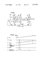
- FIG. 10 is a circuit diagram showing a common arrangement of such an internal reset circuit as described above.
- the internal reset circuit comprises series-connected capacitor C5 and N channel MOS transistor Q19 provided between a power supply Vcc and ground GND, a delay circuit 20, a latch circuit which is a reverse parallel circuit including inverters 22 and 23 provided between the node between capacitor C5 and transistor Q19 and delay circuit 20, and series-connected inverter 24 and delay circuit 21 provided between delay circuit 20 and the gate of the transistor Q19.
- An output ⁇ POR of the internal reset circuit is extracted from the output end of inverter 24.
- FIG. 11 is a timing chart explaining the operation of the internal reset circuit.
- the potential at node 17, after being delayed by delay circuit 20, is inputted to inverter 24. Therefore, the potential at node 17 appears at an input end 18 of inverter 24 with a the delay time ⁇ 1 in delay circuit 20, as shown in FIG; 11(d). Since inverter 24 inverts the output potential of delay circuit 20 to be outputted, the output potential of inverter 24, that is, the output ⁇ POR of the internal reset circuit rises to a high level upon the turning-on of the power supply as shown in FIG. 11 (e).
- inverter 24 The output of inverter 24 is applied to the predetermined internal circuit and it is also delayed by delay circuit 21.
- the delayed output is applied to gate 19 of transistor Q19.
- the potential at gate 19 of transistor Q19 accordingly attains a high level later than the output potential of inverter 24 does with a delay time ⁇ 2 in delay circuit 21, as shown in FIG. 11 (f).
- transistor Q19 When the potential at gate 19 attains a high level, transistor Q19 conducts. As a result, the potential at node 16 drops from the high level to a low level in response to a low potential at ground GND. Namely, the potential at node 16, after once attaining a high level upon the turning-on of the power supply, is maintained at a high level for the period corresponding to the sum of the delay times ⁇ 1 and ⁇ 2 in delay circuits 20 and 21, respectively and then the potential attains a low level (see FIG. 11 (b)).
- the potential at node 17 is delayed by delay circuit 20 and then inverted by inverter 24, as described above. Therefore, the potential at input end 18 of inverter 24 rises later than the potential at node 17 does with the delay time ⁇ 1 after the turning-on of the power supply (see FIG. 11 (d)).
- the output ⁇ POR of inverter 24 rises to a high level upon the turning-on of the power supply and then after being maintained at a high level for a period corresponding to the delay time ⁇ 1 in delay circuit 20, the output drops to a low level (see FIG. 11 (e)).
- the output potential of inverter 24 is fed back to gate 19 of transistor Q19 through delay circuit 21.
- the potential at gate 19 of transistor Q19 accordingly once attains a high level for a certain period upon the turning-on of the power supply, and then attains a low level.
- the potential at gate 19 drops from a high level to the low level, the transistor Q19 being conductive until then again becomes non-conductive.
- the potential at node 16 is fixed to a low level hereinafter in response to the high level potential latched in node 17.
- the potentials at node 16, gate 19 and the output end of inverter 24 are maintained at the low level.
- the potentials at node 17 and the input end 18 of inverter 24 are maintained at the high level.
- the signal attaining a high level for a certain period that is, one shot pulse is inputted from inverter 24 upon a turning-on of the power supply.
- the one pulse is a power-on-reset signal POR for resetting the predetermined internal circuit.
- FIG. 12 is a circuit diagram showing in more detail the internal reset circuit shown in FIG. 10.
- FIG. 13 is a timing chart explaining the operations of the internal reset circuit of FIG. 10 when a power supply voltage is slow in rising after a power supply is turned on. Referring to FIG.
- inverters 22, 23 and 24 comprise series-connected P channel MOS transistor Q26 and N channel MOS transistor Q27, series-connected P channel MOS transistor Q24 and N channel MOS transistor Q25 and series-connected P-channel MOS transistor Q28 and N channel MOS transistor Q29, respectively, each transistor being provided between a power supply Vcc and ground GND.
- the potential at input end 18 of inverter 24 also slowly rises accordingly as shown in FIG. 13 (d). Namely, the potential at the input end 18 is maintained at a low potential allowing transistor Q28 constituting inverter 24 to conduct for a long period after the turning-on of the power supply. As a result, the output potential at inverter 24 and the potential at gate 19 of transistor Q19 also rise slowly as the rise of the power supply voltage as shown in FIGS. 13 (e) and (f), respectively.
- transistor Q19 When the potential at gate 19 of transistor Q19 reaches a threshold voltage of transistor Q19, transistor Q19 conducts to lower the potential at node 16 to the low potential of ground GND. Accordingly, while the potential at node 16 gradually rises after the turning-on of the power supply, it is pulled down to a low level before rising to a high level.
- transistor Q26 constituting inverter 22 becomes more fully conductive.
- the potential at node 17 rises to the then power supply voltage and thereafter, it rises at approximately the same rise rate as that of the power supply potential to duly attain a high level.
- the potential change of the node 17 appears at input end 18 of inverter 24 with the delay time ⁇ 1, whereby the potential at the input end 18 similarly changes to the potential at node 17.
- the potential at input end 18 reaches the threshold voltage of inverter 24, thereby pulling down the increasing output potential at inverter 24 to a low level. Consequently, the output potential of inverter 24 gradually rises after the turning-on of the power supply.
- transistor Q25 Since transistor Q25 is maintained in an on state in response to the high level potential latched in node 17 after transistor Q19 becomes non-conductive, the potentials at node 16, gate 19 and the output end of inverter 24 are maintained at a low level and the potentials at node 17 and input end 18 attain a high level in due course and it is fixed to the level.
- the potential of the output (output ⁇ POR of this internal reset circuit) of inverter 24 takes the waveform as shown in FIG. 13 (e) not including the complete high level portion for a certain period after a turning-on of the power supply as shown in FIG. 11 (e).
- the internal circuit to be reset by the output signal of the internal reset circuit generating a high level one shot pulse is reset for a period when a high level signal is applied from the internal reset circuit as a result of a potential level at a predetermined node therein forced to a level to be obtained in an initial state.
- such one shot pulse should be generated as having a level and a width allowing the predetermined node to be fully forced to the level to be obtained in the initial state. Therefore, when the rise rate of the power supply potential after the turning-on of the power supply is slow, it sometimes occurs that a sufficient one shot pulse can not be obtained from the conventional internal reset circuit for resetting the internal circuit. Consequently, according to a conventional internal reset circuit, an internal circuit might not be fully reset depending on a rise rate of a power supply voltage to cause malfunction of the device.
- an object of the present invention is to provide a semiconductor integrated circuit device having an internal circuit reliably reset irrespective of a rise rate of a power supply potential at a turning-on of a power supply.
- Another object of the present invention is to provide a semiconductor integrated circuit device comprising an internal reset circuit reliably generating one shot pulse of a predetermined potential level irrespective of a rise rate of a power supply potential at a turning-on of a power supply.
- a further object of the present invention is to provide a semiconductor integrated circuit device in which no malfunction due to erroneous resetting of an internal circuit occurs even when no one shot pulse is generated from an internal reset circuit at a turning-on of a power supply.
- the semiconductor integrated circuit device includes an internal circuit operative in response to an internal clock signal and an initialization circuit for initializing the internal circuit based on a power supply potential and the internal clock signal.
- the initialization circuit includes a first node coupled to the power supply potential and which potential changes following a change in the power supply potential upon a turning-on of the power supply, a first circuit element coupled to the first node so as to contribute to the potential change of the first node, and a reset signal generating circuit for generating a reset signal for initializing the internal circuit in response to a predetermined potential at the first node after the turning-on of the power supply and the internal clock signal.
- the internal circuit includes a function circuit having a second node and functioning in response to the potential at the second node, an enforcing circuit for enforcing the potential at the second node to the potential required for initialization of the function circuit in response to the reset circuit generated by the reset signal generating circuit, and a second circuit element coupled to the second node so as to contribute to the potential change of the second node, which internal circuit being structured such that when the reset signal generating circuit generates no reset signal after the turning-on of the power supply, the potential at the second node attains the necessary potential for initializing the function circuit by varying the first circuit element and the second circuit element in contribution to the potential changes of the first node and the second node, respectively.
- the reset signal generating circuit in the semiconductor integrated circuit device is structured, differently from the conventional one, so as to generate the reset signal in response to the potential at the first node coupled to the power supply potential and which potential changes following the potential change of the power supply upon the turning-on of the power supply and the potential of the internal clock signal. Therefore, irrespective of the rise rate of the power supply potential after the turning-on of the power supply, when the potential at the first node attains the predetermined potential, the reset signal generating circuit generates a reset signal without fail.
- the degrees of contribution of the first circuit element and the second circuit element to the potential changes at the first node and the second node, respectively, is settled such that when the reset signal generating circuit generates no reset signal even after the turning-on of the power supply, the potential at the second node attains the necessary potential for resetting the function circuit, even if the reset signal generating circuit generates no reset signal when the potential at the first node is not the predetermined one, the potential at the second node is at the predetermined potential to be settled after the turning-on of the power supply, thereby causing no malfunction of the device.
- the reset signal generating circuit includes a one shot pulse generating circuit for outputting a single pulse synchronizing with the first level inversion of the internal clock signal after the turning-on of the power supply in response to the predetermined potential at the first node and the internal clock signal.
- the first circuit element includes a first MOS transistor coupling the first node to the power supply potential and a second MOS transistor coupling the first node to the ground potential
- the second circuit element includes a third MOS transistor coupling the second node to the power supply potential
- a fourth MOS transistor coupling the second node to the ground potential, the MOS transistors different from the first and the second MOS transistors in characteristics such as a threshold voltage and a channel length and the like.
- the first circuit element includes a first capacitor coupling the first node to the power supply potential and the second circuit element includes a second capacitor coupling the second node to the ground potential.
- the enforcing circuit includes a MOS transistor provided between the second node and ground and having a gate receiving the output of the reset signal generating circuit.
- circuit arrangement is the same with respect to the first node and the second node.
- the one shot pulse generating circuit includes a first inverter provided between the power supply and ground for inverting the potential at the first node, a holding circuit for holding the potential at the first node in response to the output of the first inverter, a two-input NOR gate inputting the output of the first inventer and the internal clock signal, and a second inverter for inverting the potential level of the first node in response to the inversion of the output potential level of the first inverter.
- the potential of the internal clock signal is inverted from the "H" level to the "L” level after the turning-on of the power supply.
- the function circuit includes, for example, an inverter receiving the potential at the second node and a MOS transistor having a gate receiving the output of the inverter and provided between ground and the second node.
- the holding circuit desirably includes a MOS transistor provided between the first node and ground and having a gate receiving the output of the first inverter.
- the function circuit includes, for example, an inverter for inverting the potential at the second node and an inverter for inverting the output of this inverter and applying the inverted output to the second node.
- the holding circuit desirably includes an inverter for inverting the output of the first inverter and applying the inverted output to the first node.
- the semiconductor integrated circuit device is a semiconductor integrated circuit device for initializing the circuit operative in response to a clock signal, the device including a node, a raising circuit for raising the potential at the node to the power supply potential upon the turning-on of the power supply, an inverting circuit for inverting the potential at the node raised by the raising circuit, a logical gate, for example an NOR gate, receiving the inversion output of the inversion circuit and the clock signal, a delay circuit for delaying the output of the logical gate by a certain time, and a lowering circuit for lowering the potential at the node to the ground potential, the output of the logical gate being applied to the circuit operative in response to the clock signal as a reset signal for initializing the circuit.
- a logical gate for example an NOR gate
- an internal node can be reset irrespective of a rise time of the power supply by reliably generating a reset signal in synchronization with an internal clock as required prior to a start of an operation of the device. Therefore, the internal circuit is more reliably reset than in the conventional one to avoid malfunction of the device caused by erroneous resetting, thereby improving the reliability of the semiconductor integrated circuit device.
- FIG. 1 is a schematic block diagram of a dual port memory according to one embodiment of the present invention.
- FIGS. 2 and 3 are circuit diagrams showing one example of the internal reset circuit for use in the dual port memory of FIG. 1.
- FIGS. 4 and 5 are timing charts explaining an operation of the internal reset circuit shown in FIGS. 2 and 3.
- FIG. 6 is a circuit diagram of a logic setting circuit desirably reset by the internal reset circuit shown in FIGS. 2 and 3.
- FIG. 7 is a circuit diagram showing one example of a latch circuit to be reset by an internal reset circuit.
- FIG. 8 is a circuit diagram showing one example of an internal reset circuit desirably resetting the latch circuit shown in FIG. 7 according to another embodiment of the present invention.
- FIG. 9 is a schematic block diagram of a dual port memory comprising a conventional internal reset circuit.
- FIGS. 10 and 12 are circuit diagrams showing the arrangements of the conventional internal reset circuits.
- FIGS. 11 and 13 are timing charts explaining an operation of the conventional internal reset circuit.
- FIG. 1 is the schematic block diagram of the dual port memory according to one embodiment of the present invention.
- the dual port memory has the same arrangement as that of the conventional dual port memory shown in FIG. 9.
- a POR generating circuit 112a provided in this dual port memory receives a clock signal ⁇ CLK generated by timing generator 111 based on, for example, an external address strobe signal RAS, to generate a reset pulse POR and outputs the same.
- the arrangements and operations of the other function blocks of this dual port memory are as described in "Description of the Background Art".
- FIG. 2 is the circuit diagram showing one example of the arrangement of the internal reset circuit for use as POR generating circuit 112a shown in FIG. 1.
- the internal reset circuit includes an inverter 25 comprising series-connected capacitor C1 and N channel MOS transistor Q1 and series-connected N channel MOS transistor Q3 and P channel MOS transistor Q4 both series-connection between power supply Vcc and ground GND.
- the connection point between capacitor C1 and transistor Q1 is connected to the input end of inverter 25, that is, the gates of transistor Q3 and Q4.
- This internal reset circuit further comprises an N channel MOS transistor Q2 provided between the input end of inverter 25 and ground GND, a two-input NOR gate 3 receiving the potential at the output end of inverter 25, that is, at the connection point between transistors Q3 and Q4, and the internal clock signal ⁇ CLK , and a delay circuit 4 provided between the output end of NOR gate 3 and a gate 5 of transistor Q1.
- the output ⁇ POR of the internal reset circuit is extracted from the output end of NOR gate 3.
- FIG. 5 is the timing chart explaining the basic operation of the internal reset circuit of the above-described arrangement.
- the potential at power supply Vcc rises to a predetermined potential (high level) as shown in FIG. 5 (a).
- the potential at the connection point between capacitor C1 and transistor Q1, that is, at the input end (node 1) of inverter 25 also rises at approximately the same rate as that of the power supply potential (see FIG. 5 (b)).
- the internal clock signal ⁇ CLK repeats level inversion at a predetermined timing after rising to a high level upon the turning-on of the power supply. While potentials at both input ends of NOR gate 3, that is, the potential of the internal clock signal ⁇ CLK and the potential at the output end of the inverter 25 are at a low level immediately after the turning-on of the power supply, one of the potentials (the potential of the internal clock signal ⁇ CLX ) instantly attains a high level.
- the output potential of NOR gate 3 that is, the potential of the output signal ⁇ POR of this internal reset circuit, which potential is supposed to rise immediately after the turning-on of the power supply when both input potentials to NOR gate 3 are at a low level as shown in FIG. 5 (e)
- the output potential of NOR gate 3 is pulled down to a low level before rising to a high level because one input potential instantly attains a high level.
- the fall of the internal clock signal ⁇ CLK causes the two input potentials to NOR gate 3 to remain at a low level until the next rise of the internal clock signal ⁇ CLK .
- the output potential of NOR gate 3 rises to a high level.
- the output potential of NOR gate 3 is fed back with a delay time in delay circuit 4 to gate 5 of transistor Q1.
- the potential at gate 5 accordingly rises to a high level later than the fall of the output potential at NOR gate 3 by the predetermined time.
- transistor Q1 is turned on, whereby the potential at node 1 falls from the high level to a low level (see FIG. 5 (b)). Consequently, transistor Q3 is replaced by transistor Q4 to be turned on in inverter 25, so that the potential at input end 2 of NOR gate 3 rises from the low level to a high level (see FIG. 5 (c)).
- one input potential to NOR gate 3 rises to a high level later than the first fall of the internal clock signal ⁇ CLK later by a time period corresponding to the delay time in delay circuit 4, whereby the potential at the output end of NOR gate 3 falls to a low level.
- the internal reset circuit outputs one shot pulse of a high level.
- this internal reset circuit generates one shot pulse of a high level just once after the turning-on of the power supply.
- the internal reset circuit is structured to generate a one shot pulse in synchronization with the first rise of the internal clock signal.
- FIGS. 3 and 4 will be an operation of this internal reset circuit when a rise rate of the power supply potential is slow after a turning-on of the power supply.
- FIG. 3 is the circuit diagram of the above-described internal reset circuit wherein the circuit arrangement of NOR gate 3 is illustrated in detail and
- FIG. 4 is the timing chart explaining an operation of the above-described internal reset circuit when the rise rate of the power supply potential is slow after a turning-on of the power supply.
- NOR gate 3 of FIG. 2 comprises series-connected P channel MOS transistors Q20 and Q21 and N channel MOS transistor Q22 provided between the power supply Vcc and ground GND, and a transistor Q23 connected in parallel to transistor Q22.
- the internal clock signal ⁇ CLK is applied to the gates of transistors Q20 and Q23.
- the output potential of NOR gate 3 that is, the potential at the node between transistors Q21 and Q23 gradually rises in response to the power supply potential as shown in FIG. 4 (e).
- transistor Q23 is turned on to pull down the output potential of NOR gate 3 to the potential of ground GND, which output potential attains a low level after the power on.
- transistor Q1 having gate 5 receiving the output potential of NOR gate 3 through delay circuit 4 and transistor Q2 having the gate receiving the potential at node 2 are off after the power on. Therefore, the potential at node 1 after the power on is determined by the power supply potential.
- transistor Q20 in place of transistor Q23 conducts in NOR gate 3. Meanwhile, the potential at node 2 is at a low level and transistor Q21 is conductive. In response to the fall of the internal clock signal ⁇ CLK , the output potential at NOR gate 3 attains a high level in response to the power supply potential which has completely risen (see FIG. 4 (e)).
- this internal reset circuit thereafter is the same as that in the case where the power supply potential rises quickly. Namely, transistor Q1 having the gate 5 receiving the output potential of NOR gate 3 through delay circuit 4 conducts, whereby the output potential of inverter 25 attains a high level to render transistor Q2 conductive. As a result, the potential at node 2 is fixed to a high level and the output potential at NOR gate 3, after attaining a low level in response to the conduction of transistor Q22, is maintained at a low level irrespective of the later level change of the internal clock signal ⁇ CLK Namely, the internal reset circuit outputs one shot pulse just once after the power on.
- the internal reset circuit outputs one shot pulse enough to reset predetermined internal circuits in FIG. 1, for example, color register 113 and write mask register 114 or the like.
- the internal clock signal ⁇ CLK dropping to a low level at a predetermined timing after completely rising in response to the power supply potential, is applied to the gate of one transistor Q20 out of P channel transistors Q20 and Q21 to raise the output potential at NOR gate 3 to a high level, while the other transistor Q21 is rendered conductive after the power on.
- both transistors Q20 and Q21 are on only for a period starting immediately after the power on and ending when the potential of the internal clock signal ⁇ CLK exceeds the threshold voltage of transistor Q20 for a period starting from the first fall of the potential of the internal clock signal and ending when the output potential of inverter 25 exceeds the threshold voltage of transistor Q21.
- the rise rate of the power supply potential after the power on is slow, the power supply potential does not completely rise in the former period, preventing the output potential at NOR gate 3 from rising to a high level.
- the output potential at NOR gate 3 rapidly rises to a high level. As a result, even if the rise rate of the power supply potential is slow, sufficient one shot pulses can be obtained.
- FIG. 6 is the circuit diagram showing one example of the logic setting circuit desirably reset by the internal reset circuit shown in FIGS. 2 and 3.
- the logic setting circuit includes an inverter 26 comprising series-connected N channel MOS transistor Q7 and P channel MOS transistor Q8 provided between the power supply Vcc and ground GND, and N channel transistors Q5, Q6 and a capacitor C2 provided in parallel between the input end of the inverter 26 and ground GND.
- a fuse 8 is provided between transistor Q6 and the power supply Vcc, the gate of transistor Q6 is connected to the output end of inverter 26, that is, to the connection point (a node 7) between transistors Q7 and Q8, (a node 7) and the gate of transistor Q5 receives an output signal ⁇ POR of the internal reset circuit. The output of this logic setting circuit is extracted from the node 7.
- RAMs, EPROMs or the like include spare memory cell arrays in addition to the memory cell arrays to be ordinarily used.
- Such a spare memory cell array is a redundancy circuit for use in preventing the decrease in yields of LSIs or the like, which circuit replaces the defective memory cell array if a part of the memory cell arrays to be ordinarily used has any defect.
- signals instructing use/non-use should be applied to the respective memory cell arrays such that defective memory cell arrays are disabled and spare memory cell arrays replacing the same are enabled.
- Such a semiconductor memory device as described above includes a logic setting circuit provided for each memory cell array for applying the instructing signal.
- a logic setting circuit generally includes a fuse as shown in FIG. 6.
- the logic setting circuit is structured to apply a signal instructing either the use or non-use after a power on based on whether the fuse is cut off or not.
- the fuse of the logic setting circuit is selectively cut off in accordance with the setting of use/non-use of each memory cell array.
- the potential at node 6 does not rise and remains at a low level even if the power is on.
- the potential at node 7 being also applied to the gate of transistor Q6, the potential at node 6 after the power on is fixed to the potential (low level) at ground GND in response to the conduction of transistor Q6.
- the potential at node 7 is maintained at a high level for instructing use or non-use.
- the potential at node 6 needs to be at a low level without fail at the power on so that the potential at node 7 reliably attains a high level after the power on when fuse 8 is disconnected.
- the potential at node 6 does not necessarily attain a potential low enough to render transistor Q8 conductive at the power on.
- transistor Q5 is provided which conducts in response to a high level one shot pulse outputted by the above-described internal reset circuit in order to render the potential at node 6 the ground potential immediately after the power on, that is, to reset.
- transistor Q5 when a high level one shot pulse is applied from the internal reset circuit after the power on, transistor Q5 conducts only for the period when transistor Q5 receives the one shot pulse, thereby rendering the potential at node 6 the potential at ground GND. Therefore, even if the potential at node 6 rises to a level for some causes which level should not be obtained at the power on, the potential is immediately returned to a level (referred to as an original level) which should be obtained at the power on. As a result, the correct instructing signal can be obtained from node 7, allowing a correct setting of use/non-use of a memory cell array.
- node 1 Comparing node 6 to be reset with node 1 determining a rise timing of the output potential of the internal circuit shown in FIG. 2, while node 6 is connected to ground GND through N channel MOS transistors Q5 and Q6, and capacitor C2, node 1 is connected to ground GND through N channel MOS transistors Q1 and Q2 and to the power supply Vcc through capacitor C1. Therefore, if such characteristics as a threshold voltage and a channel length are the same for transistors Q5 and Q6, and transistors Q1 and Q2, the potential at node 1 is liable to be pulled up to the power supply potential Vcc and that at node 6 is liable to be pulled down to the ground potential GND. Namely, node 1 more easily attains a high potential than the node 6.
- the potential at node 6 of the logic setting circuit is also at a low level. If the potential at node 6 is low herein, it is not necessary for the logic setting circuit to be reset.
- the potential at node 2 needs to attain a high level when the internal clock signal ⁇ CLK falls so that the output of NOR gate 3 reliably rises after the power on.
- node 6 to be reset is at a low level at any time. In such a case, even if a sufficient reset pulse is not outputted, no malfunction occurs in the function part coupled to the circuit to be reset.
- the internal reset circuit outputs sufficient one shot pulses of a high level irrespective of the rise rate of the power supply potential, as described above.
- the internal reset circuit reliably outputs one shot pulses when the node 6 to be reset requires resetting at a fall of an internal clock signal.
- a semiconductor integrated circuit device requiring an internal clock signal is generally structured to start its operation in response to the first fall of the internal clock signal after a power on.
- the internal reset circuit shown in FIG. 2 is capable of rendering the potential at node 6 to be reset at the original level irrespective of a potential attained by node 1 after the start of the operation of the device.
- a balance of a liability of node 6 to be reset to attain a high potential and that of internal node 1 of the internal reset circuit determining a rise timing of the output potential of the internal reset circuit to attain a high potential can be controlled by controlling coupling capacitances between the respective nodes and a higher potential source and a lower potential source, characteristics of a transistor connected for supplying the respective nodes with the output potential of the lower potential source (or the output potential of the higher potential source) or the like. The characteristics of these nodes are affected by the characteristics of all the circuit elements connected to the respective nodes.
- arrangements of the internal reset circuit and a circuit to be reset by the same are desirably similar to each other with respect to the respective nodes. For example, assuming that the capacitors C1 and C2 and the fuse 8 are removed in the above-described embodiment, the arrangement of the internal reset circuit with respect to node 1 and the arrangement of the logic setting circuit with respect to node 6 are the same.
- the circuit arrangements with respect to the node determining a generation timing of one shot pulses in the internal reset circuit for use as POR generating circuit 112a shown in FIG. 1 are desirably similar to that with respect to the node to be reset in a color register 113 and a write mask register 114.
- FIG. 7 is the circuit diagram showing one example of a latch circuit to be reset immediately after a power on and shows a circuit arrangement with respect to the node to be reset in each of color register 113 and write mask register 114 of FIG. 1.
- the latch circuit includes N channel MOS transistors Q14, Q15 and Q17, P channel MOS transistors Q16 and Q18 and a capacitor C4, showing the arrangement of the logic setting circuit shown in FIG. 6 with fuse 8 replaced by P channel MOS transistor Q16.
- the gate of transistor Q16 is connected to the gate of transistor Q15 for receiving a potential at a connection point between transistors Q17 and Q18, which point is the output end of the latch circuit.
- no transmission path is formed for the potential at the power supply Vcc to node 14 (corresponding to node 6 in the logic setting circuit shown in FIG. 6) unless transistor Q16 conducts.
- the potential at node 14 needs to be reset to a low level after a power on because the potential at node 14 might rise for some reasons.
- transistor Q14 conducts in response to a high level one shot pulse from the internal reset circuit after a power on, thereby forcing the potential at node 14 to ground potential.
- FIG. 8 is the circuit diagram showing one example of an arrangement of a preferred internal reset circuit for resetting the above-described latch circuit, which is another embodiment of the present invention.
- the internal reset circuit is provided with a P channel MOS transistor Q11 between node 1 and power supply Vcc, different from that shown in FIG. 2.
- the gate of transistor Q11 is connected with the gate of transistor Q2.
- transistors Q2 and Q11 constitute an inverter 27. The reason for this provision is for facilitating control of a difference between the liability of node 1 to attain a high potential and the liability of node 14 to be reset to attain a high potential by making the circuit arrangement with respect to node 14 in the latch circuit to be reset the same as the circuit arrangement with respect to node 1 in the internal reset circuit
- transistor Q11 when the potential at one input end 2 of inverter 3 attains a low level, transistor Q11 is turned on and transistor Q2 is turned off, so that the power supply potential is transmitted to node 1 through capacitor C1 and transistor Q11. Namely, transistor Q11 serves to reliably supply a high potential to node 1.
- the basic operations of the internal reset circuit are the same as those of the internal reset circuit shown in FIG. 2, by which one shot pulses can be reliably generated even at a slow rise rate of the power supply potential.
- capacitor C1 is provided between node 1 and the power supply Vcc
- capacitor C4 is provided between the node to be reset and ground GND in the circuit to be reset, whereby node 1 is more liable to attain a high level than node 14 as long as other circuit elements connected to node 1 and other circuit elements connected to node 14 have the same characteristics.
- node 14 to be reset attains a high level without fail. Therefore no malfunction occurs in the circuit part operative in response to the potential at node 15 even if transistor Q14 does not receive sufficient one shot pulses.
- Each of color register 113 and write mask register 114 to be reset in the dual port memory of FIG. 1 is a circuit having latching functions for temporality storing data, which circuit has such arrangement as shown in FIG. 7.
- the internal reset circuit having the arrangement shown in FIG. 8 is desirably used as POR generating circuit 112a in the dual port memory shown in FIG. 1.
- the internal reset circuit according to the present invention can be applied to a case where the potential should be high level at the power on.
- any of the internal reset circuits described in the above-described embodiment is structured so as to output one shot pulses at a high level, it can be structured to output one shot pulses of a low level by adding another inverter to the output stage of the internal reset circuit if the circuit to be reset is structured so as to be reset in response to an external signal of a low level.
Landscapes
- Engineering & Computer Science (AREA)
- Theoretical Computer Science (AREA)
- Physics & Mathematics (AREA)
- General Engineering & Computer Science (AREA)
- General Physics & Mathematics (AREA)
- Dram (AREA)
- Static Random-Access Memory (AREA)
- Semiconductor Memories (AREA)
- Electronic Switches (AREA)
Applications Claiming Priority (2)
| Application Number | Priority Date | Filing Date | Title |
|---|---|---|---|
| JP1340203A JP2724893B2 (ja) | 1989-12-28 | 1989-12-28 | 半導体集積回路装置 |
| JP1-340203 | 1989-12-28 |
Publications (1)
| Publication Number | Publication Date |
|---|---|
| US5177375A true US5177375A (en) | 1993-01-05 |
Family
ID=18334694
Family Applications (1)
| Application Number | Title | Priority Date | Filing Date |
|---|---|---|---|
| US07/628,696 Expired - Fee Related US5177375A (en) | 1989-12-28 | 1990-12-14 | Power on reset circuit for semiconductor integrated circuit device |
Country Status (3)
| Country | Link |
|---|---|
| US (1) | US5177375A (ja) |
| JP (1) | JP2724893B2 (ja) |
| DE (1) | DE4041945C2 (ja) |
Cited By (69)
| Publication number | Priority date | Publication date | Assignee | Title |
|---|---|---|---|---|
| US5345110A (en) * | 1993-04-13 | 1994-09-06 | Micron Semiconductor, Inc. | Low-power fuse detect and latch circuit |
| US5374923A (en) * | 1991-12-16 | 1994-12-20 | Mitsubishi Denki Kabushiki Kaisha | Power-on detecting circuit |
| US5376835A (en) * | 1992-10-22 | 1994-12-27 | Advanced Micro Devices, Inc. | Power-on reset circuit |
| US5408139A (en) * | 1992-11-09 | 1995-04-18 | Mitsubishi Denki Kabushiki Kaisha | Semiconductor integrated circuit device having circuit for generating power-on reset signal |
| US5436586A (en) * | 1990-07-31 | 1995-07-25 | Mitsubishi Denki Kabushiki Kaisha | Semiconductor integrated circuit apparatus including supply voltage conversion circuit |
| EP0665488A2 (en) * | 1994-01-27 | 1995-08-02 | Rockwell International Corporation | Supply sensing circuit with power-on reset detection |
| US5469099A (en) * | 1992-06-17 | 1995-11-21 | Mitsubishi Denki Kabushiki Kaisha | Power-on reset signal generator and operating method thereof |
| US5477176A (en) * | 1994-06-02 | 1995-12-19 | Motorola Inc. | Power-on reset circuit for preventing multiple word line selections during power-up of an integrated circuit memory |
| US5498989A (en) * | 1994-04-19 | 1996-03-12 | Xilinx, Inc. | Integrated circuit one shot with extended length output pulse |
| US5528184A (en) * | 1992-06-26 | 1996-06-18 | Sgs-Thomson Microelectronics, S.R.L. | Power-on reset circuit having a low static power consumption |
| US5570050A (en) * | 1994-03-08 | 1996-10-29 | Intel Corporation | Zero standby current power-up reset circuit |
| US5659259A (en) * | 1996-04-12 | 1997-08-19 | Hewlett-Packard Company | Circuit and method of sensing small voltage changes on highly capacitively loaded electronic signals |
| US5760624A (en) * | 1995-04-28 | 1998-06-02 | Altera Corporation | Power-on reset circuit with hysteresis |
| US5864251A (en) * | 1994-10-28 | 1999-01-26 | Cypress Semiconductor Corporation | Method and apparatus for self-resetting logic circuitry |
| US5889728A (en) * | 1998-02-10 | 1999-03-30 | Cypress Semiconductor Corporation | Write control method for memory devices |
| US5933032A (en) * | 1995-12-29 | 1999-08-03 | Cypress Semiconductor Corp. | Apparatus and method for generating a pulse signal |
| US5936977A (en) * | 1997-09-17 | 1999-08-10 | Cypress Semiconductor Corp. | Scan path circuitry including a programmable delay circuit |
| US5953285A (en) * | 1997-09-17 | 1999-09-14 | Cypress Semiconductor Corp. | Scan path circuitry including an output register having a flow through mode |
| US6005423A (en) * | 1994-02-10 | 1999-12-21 | Xilinx, Inc. | Low current power-on reset circuit |
| US6075718A (en) * | 1997-03-18 | 2000-06-13 | Stmicroelectronics, S.R.L. | Method and device for reading a non-erasable memory cell |
| US6081475A (en) * | 1998-02-10 | 2000-06-27 | Cypress Semiconductor Corporation | Write control apparatus for memory devices |
| US6087890A (en) * | 1998-04-14 | 2000-07-11 | Lg Semicon Co., Ltd. | Redundancy fuse read circuit |
| US6100747A (en) * | 1994-05-30 | 2000-08-08 | Stmicroelectronics, S.R.L. | Device for selecting design options in an integrated circuit |
| US6115836A (en) * | 1997-09-17 | 2000-09-05 | Cypress Semiconductor Corporation | Scan path circuitry for programming a variable clock pulse width |
| US6184731B1 (en) * | 1998-05-11 | 2001-02-06 | Mitsumi Electric Co., Ltd. | Reset signal generation circuit |
| US6215170B1 (en) | 1996-12-31 | 2001-04-10 | Stmicroelectronics, Inc. | Structure for single conductor acting as ground and capacitor plate electrode using reduced area |
| US6222393B1 (en) | 1999-07-20 | 2001-04-24 | Cypress Semiconductor Corporation | Apparatus and method for generating a pulse signal |
| US6236249B1 (en) * | 1998-06-12 | 2001-05-22 | Samsung Electronics Co., Ltd. | Power-on reset circuit for a high density integrated circuit |
| US6252442B1 (en) * | 1996-09-19 | 2001-06-26 | Sgs-Thomson Microelectronics S.A. | Electronic circuit provided with a neutralization device |
| US6362669B1 (en) * | 2000-04-10 | 2002-03-26 | Xilinx, Inc. | Structure and method for initializing IC devices during unstable power-up |
| KR100333666B1 (ko) * | 1999-06-30 | 2002-04-24 | 박종섭 | 다양한 파워-온 신호에 대하여 리셋신호를 생성하는 파워-온리셋회로 |
| US6566919B2 (en) * | 2000-11-29 | 2003-05-20 | Silicon Storage Technology, Inc. | Power on circuit for generating reset signal |
| US6737895B2 (en) * | 2001-07-31 | 2004-05-18 | Infineon Technologies Ag | Control signal generating device for driving a plurality of circuit units |
| US20060026349A1 (en) * | 2004-07-30 | 2006-02-02 | International Business Machines Corporaiton | System, method and storage medium for providing a serialized memory interface with a bus repeater |
| US20060036826A1 (en) * | 2004-07-30 | 2006-02-16 | International Business Machines Corporation | System, method and storage medium for providing a bus speed multiplier |
| US20060095671A1 (en) * | 2004-10-29 | 2006-05-04 | International Business Machines Corporation | System, method and storage medium for providing data caching and data compression in a memory subsystem |
| US20060095629A1 (en) * | 2004-10-29 | 2006-05-04 | International Business Machines Corporation | System, method and storage medium for providing a service interface to a memory system |
| US20060095703A1 (en) * | 2004-10-29 | 2006-05-04 | International Business Machines Corporation | System, method and storage medium for bus calibration in a memory subsystem |
| US20060095620A1 (en) * | 2004-10-29 | 2006-05-04 | International Business Machines Corporation | System, method and storage medium for merging bus data in a memory subsystem |
| US20060095701A1 (en) * | 2004-10-29 | 2006-05-04 | International Business Machines Corporation | System, method and storage medium for a memory subsystem with positional read data latency |
| US20060107175A1 (en) * | 2004-10-29 | 2006-05-18 | International Business Machines Corporation | System, method and storage medium for providing fault detection and correction in a memory subsystem |
| US20060107186A1 (en) * | 2004-10-29 | 2006-05-18 | International Business Machines Corporation | System, method and storage medium for providing a high speed test interface to a memory subsystem |
| US20060117233A1 (en) * | 2004-10-29 | 2006-06-01 | International Business Machines Corporation | System, Method and storage medium for testing a memory module |
| US20060132183A1 (en) * | 2004-12-22 | 2006-06-22 | Dong-Jin Lim | Semiconductor device |
| US20070101086A1 (en) * | 2005-10-31 | 2007-05-03 | International Business Machines Corporation | System, method and storage medium for deriving clocks in a memory system |
| US20070160053A1 (en) * | 2005-11-28 | 2007-07-12 | Coteus Paul W | Method and system for providing indeterminate read data latency in a memory system |
| US7299313B2 (en) | 2004-10-29 | 2007-11-20 | International Business Machines Corporation | System, method and storage medium for a memory subsystem command interface |
| US20070276976A1 (en) * | 2006-05-24 | 2007-11-29 | International Business Machines Corporation | Systems and methods for providing distributed technology independent memory controllers |
| US20070276977A1 (en) * | 2006-05-24 | 2007-11-29 | International Business Machines Corporation | Systems and methods for providing memory modules with multiple hub devices |
| US20070288707A1 (en) * | 2006-06-08 | 2007-12-13 | International Business Machines Corporation | Systems and methods for providing data modification operations in memory subsystems |
| US20080005479A1 (en) * | 2006-05-22 | 2008-01-03 | International Business Machines Corporation | Systems and methods for providing remote pre-fetch buffers |
| US20080034148A1 (en) * | 2006-08-01 | 2008-02-07 | International Business Machines Corporation | Systems and methods for providing performance monitoring in a memory system |
| US20080040562A1 (en) * | 2006-08-09 | 2008-02-14 | International Business Machines Corporation | Systems and methods for providing distributed autonomous power management in a memory system |
| US20080040563A1 (en) * | 2006-08-10 | 2008-02-14 | International Business Machines Corporation | Systems and methods for memory module power management |
| US20080098277A1 (en) * | 2006-10-23 | 2008-04-24 | International Business Machines Corporation | High density high reliability memory module with power gating and a fault tolerant address and command bus |
| US20080094811A1 (en) * | 2006-10-23 | 2008-04-24 | International Business Machines Corporation | High density high reliability memory module with a fault tolerant address and command bus |
| US20080115137A1 (en) * | 2006-08-02 | 2008-05-15 | International Business Machines Corporation | Systems and methods for providing collision detection in a memory system |
| US20080122026A1 (en) * | 2006-11-29 | 2008-05-29 | International Business Machines Corporation | Structure for creation of a programmable device |
| US20080133797A1 (en) * | 2004-07-30 | 2008-06-05 | International Business Machines Corporation | System, method and storage medium for a multi-mode memory buffer device |
| US20080162991A1 (en) * | 2007-01-02 | 2008-07-03 | International Business Machines Corporation | Systems and methods for improving serviceability of a memory system |
| US20080183903A1 (en) * | 2007-01-29 | 2008-07-31 | International Business Machines Corporation | Systems and methods for providing dynamic memory pre-fetch |
| US7490217B2 (en) | 2006-08-15 | 2009-02-10 | International Business Machines Corporation | Design structure for selecting memory busses according to physical memory organization information stored in virtual address translation tables |
| US20090119114A1 (en) * | 2007-11-02 | 2009-05-07 | David Alaniz | Systems and Methods for Enabling Customer Service |
| US7539842B2 (en) | 2006-08-15 | 2009-05-26 | International Business Machines Corporation | Computer memory system for selecting memory buses according to physical memory organization information stored in virtual address translation tables |
| US7539800B2 (en) | 2004-07-30 | 2009-05-26 | International Business Machines Corporation | System, method and storage medium for providing segment level sparing |
| US7606988B2 (en) | 2007-01-29 | 2009-10-20 | International Business Machines Corporation | Systems and methods for providing a dynamic memory bank page policy |
| US20100277150A1 (en) * | 2008-01-11 | 2010-11-04 | Ricoh Company, Ltd. | Semiconductor device and manufacturing method thereof |
| US8344767B2 (en) | 2010-10-14 | 2013-01-01 | Fairchild Semiconductor Corporation | Low power power-on-reset (POR) circuit |
| US20160239062A1 (en) * | 2013-10-02 | 2016-08-18 | Lg Electronics Inc. | Image display apparatus and method for controlling same |
Families Citing this family (3)
| Publication number | Priority date | Publication date | Assignee | Title |
|---|---|---|---|---|
| JP2994168B2 (ja) * | 1993-03-10 | 1999-12-27 | 日本電気株式会社 | 初期状態設定回路 |
| KR100231139B1 (ko) * | 1996-08-28 | 1999-11-15 | 문정환 | 리세트 신호 발생 회로 |
| KR100376871B1 (ko) * | 2000-11-28 | 2003-03-19 | 주식회사 하이닉스반도체 | 파워 업 신호 발생기 |
Citations (8)
| Publication number | Priority date | Publication date | Assignee | Title |
|---|---|---|---|---|
| US4140930A (en) * | 1976-07-30 | 1979-02-20 | Sharp Kabushiki Kaisha | Voltage detection circuit composed of at least two MOS transistors |
| EP0150480A2 (en) * | 1984-01-16 | 1985-08-07 | Itt Industries, Inc. | Power-on reset pulse generator |
| DE3515611A1 (de) * | 1985-04-30 | 1986-10-30 | Siemens AG, 1000 Berlin und 8000 München | Verfahren und anordnung zum einstellen vorgegebener startverhaeltnisse in einem mikrorechner |
| US4716302A (en) * | 1986-12-22 | 1987-12-29 | Motorola, Inc. | Identity circuit for an integrated circuit using a fuse and transistor enabled by a power-on reset signal |
| US4788454A (en) * | 1986-07-21 | 1988-11-29 | Oki Electric Industry Co., Ltd. | Power-on reset circuit |
| EP0303257A1 (en) * | 1987-08-13 | 1989-02-15 | Kabushiki Kaisha Toshiba | Reset signal generating circuit |
| US4886984A (en) * | 1987-03-27 | 1989-12-12 | Nec Corporation | Prohibition circuit upon power-on event |
| US4933902A (en) * | 1987-07-23 | 1990-06-12 | Mitsubishi Denki Kabushiki Kaisha | Method of and apparatus for reducing current of semiconductor memory device |
Family Cites Families (5)
| Publication number | Priority date | Publication date | Assignee | Title |
|---|---|---|---|---|
| JPS5437939B2 (ja) * | 1974-08-30 | 1979-11-17 | ||
| JPS56149623A (en) * | 1980-04-22 | 1981-11-19 | Mitsubishi Electric Corp | Reset circuit |
| JPS5845695A (ja) * | 1981-09-10 | 1983-03-16 | Nec Corp | 絶縁ゲ−ト型記憶回路 |
| JPS61180997A (ja) * | 1985-02-06 | 1986-08-13 | Nec Corp | 半導体記憶装置 |
| JP2703890B2 (ja) * | 1986-11-27 | 1998-01-26 | 日本電気株式会社 | 半導体集積回路 |
-
1989
- 1989-12-28 JP JP1340203A patent/JP2724893B2/ja not_active Expired - Lifetime
-
1990
- 1990-12-14 US US07/628,696 patent/US5177375A/en not_active Expired - Fee Related
- 1990-12-27 DE DE4041945A patent/DE4041945C2/de not_active Expired - Fee Related
Patent Citations (8)
| Publication number | Priority date | Publication date | Assignee | Title |
|---|---|---|---|---|
| US4140930A (en) * | 1976-07-30 | 1979-02-20 | Sharp Kabushiki Kaisha | Voltage detection circuit composed of at least two MOS transistors |
| EP0150480A2 (en) * | 1984-01-16 | 1985-08-07 | Itt Industries, Inc. | Power-on reset pulse generator |
| DE3515611A1 (de) * | 1985-04-30 | 1986-10-30 | Siemens AG, 1000 Berlin und 8000 München | Verfahren und anordnung zum einstellen vorgegebener startverhaeltnisse in einem mikrorechner |
| US4788454A (en) * | 1986-07-21 | 1988-11-29 | Oki Electric Industry Co., Ltd. | Power-on reset circuit |
| US4716302A (en) * | 1986-12-22 | 1987-12-29 | Motorola, Inc. | Identity circuit for an integrated circuit using a fuse and transistor enabled by a power-on reset signal |
| US4886984A (en) * | 1987-03-27 | 1989-12-12 | Nec Corporation | Prohibition circuit upon power-on event |
| US4933902A (en) * | 1987-07-23 | 1990-06-12 | Mitsubishi Denki Kabushiki Kaisha | Method of and apparatus for reducing current of semiconductor memory device |
| EP0303257A1 (en) * | 1987-08-13 | 1989-02-15 | Kabushiki Kaisha Toshiba | Reset signal generating circuit |
Cited By (130)
| Publication number | Priority date | Publication date | Assignee | Title |
|---|---|---|---|---|
| US5436586A (en) * | 1990-07-31 | 1995-07-25 | Mitsubishi Denki Kabushiki Kaisha | Semiconductor integrated circuit apparatus including supply voltage conversion circuit |
| US5374923A (en) * | 1991-12-16 | 1994-12-20 | Mitsubishi Denki Kabushiki Kaisha | Power-on detecting circuit |
| US5469099A (en) * | 1992-06-17 | 1995-11-21 | Mitsubishi Denki Kabushiki Kaisha | Power-on reset signal generator and operating method thereof |
| US5528184A (en) * | 1992-06-26 | 1996-06-18 | Sgs-Thomson Microelectronics, S.R.L. | Power-on reset circuit having a low static power consumption |
| US5376835A (en) * | 1992-10-22 | 1994-12-27 | Advanced Micro Devices, Inc. | Power-on reset circuit |
| US5408139A (en) * | 1992-11-09 | 1995-04-18 | Mitsubishi Denki Kabushiki Kaisha | Semiconductor integrated circuit device having circuit for generating power-on reset signal |
| US5345110A (en) * | 1993-04-13 | 1994-09-06 | Micron Semiconductor, Inc. | Low-power fuse detect and latch circuit |
| EP0665488A2 (en) * | 1994-01-27 | 1995-08-02 | Rockwell International Corporation | Supply sensing circuit with power-on reset detection |
| US5463336A (en) * | 1994-01-27 | 1995-10-31 | Rockwell International Corporation | Supply sensing power-on reset circuit |
| EP0665488A3 (en) * | 1994-01-27 | 1999-01-27 | Rockwell International Corporation | Supply sensing circuit with power-on reset detection |
| US6005423A (en) * | 1994-02-10 | 1999-12-21 | Xilinx, Inc. | Low current power-on reset circuit |
| US5570050A (en) * | 1994-03-08 | 1996-10-29 | Intel Corporation | Zero standby current power-up reset circuit |
| US5498989A (en) * | 1994-04-19 | 1996-03-12 | Xilinx, Inc. | Integrated circuit one shot with extended length output pulse |
| US6100747A (en) * | 1994-05-30 | 2000-08-08 | Stmicroelectronics, S.R.L. | Device for selecting design options in an integrated circuit |
| US5477176A (en) * | 1994-06-02 | 1995-12-19 | Motorola Inc. | Power-on reset circuit for preventing multiple word line selections during power-up of an integrated circuit memory |
| US5864251A (en) * | 1994-10-28 | 1999-01-26 | Cypress Semiconductor Corporation | Method and apparatus for self-resetting logic circuitry |
| US5760624A (en) * | 1995-04-28 | 1998-06-02 | Altera Corporation | Power-on reset circuit with hysteresis |
| US5933032A (en) * | 1995-12-29 | 1999-08-03 | Cypress Semiconductor Corp. | Apparatus and method for generating a pulse signal |
| US5659259A (en) * | 1996-04-12 | 1997-08-19 | Hewlett-Packard Company | Circuit and method of sensing small voltage changes on highly capacitively loaded electronic signals |
| US6252442B1 (en) * | 1996-09-19 | 2001-06-26 | Sgs-Thomson Microelectronics S.A. | Electronic circuit provided with a neutralization device |
| US6215170B1 (en) | 1996-12-31 | 2001-04-10 | Stmicroelectronics, Inc. | Structure for single conductor acting as ground and capacitor plate electrode using reduced area |
| US6075718A (en) * | 1997-03-18 | 2000-06-13 | Stmicroelectronics, S.R.L. | Method and device for reading a non-erasable memory cell |
| US5936977A (en) * | 1997-09-17 | 1999-08-10 | Cypress Semiconductor Corp. | Scan path circuitry including a programmable delay circuit |
| US5953285A (en) * | 1997-09-17 | 1999-09-14 | Cypress Semiconductor Corp. | Scan path circuitry including an output register having a flow through mode |
| US6115836A (en) * | 1997-09-17 | 2000-09-05 | Cypress Semiconductor Corporation | Scan path circuitry for programming a variable clock pulse width |
| US6286118B1 (en) | 1997-09-17 | 2001-09-04 | Cypress Semiconductor Corporation | Scan path circuitry including a programmable delay circuit |
| US5889728A (en) * | 1998-02-10 | 1999-03-30 | Cypress Semiconductor Corporation | Write control method for memory devices |
| US6081475A (en) * | 1998-02-10 | 2000-06-27 | Cypress Semiconductor Corporation | Write control apparatus for memory devices |
| US6087890A (en) * | 1998-04-14 | 2000-07-11 | Lg Semicon Co., Ltd. | Redundancy fuse read circuit |
| US6184731B1 (en) * | 1998-05-11 | 2001-02-06 | Mitsumi Electric Co., Ltd. | Reset signal generation circuit |
| US6236249B1 (en) * | 1998-06-12 | 2001-05-22 | Samsung Electronics Co., Ltd. | Power-on reset circuit for a high density integrated circuit |
| KR100333666B1 (ko) * | 1999-06-30 | 2002-04-24 | 박종섭 | 다양한 파워-온 신호에 대하여 리셋신호를 생성하는 파워-온리셋회로 |
| US6222393B1 (en) | 1999-07-20 | 2001-04-24 | Cypress Semiconductor Corporation | Apparatus and method for generating a pulse signal |
| US6362669B1 (en) * | 2000-04-10 | 2002-03-26 | Xilinx, Inc. | Structure and method for initializing IC devices during unstable power-up |
| US6566919B2 (en) * | 2000-11-29 | 2003-05-20 | Silicon Storage Technology, Inc. | Power on circuit for generating reset signal |
| US6737895B2 (en) * | 2001-07-31 | 2004-05-18 | Infineon Technologies Ag | Control signal generating device for driving a plurality of circuit units |
| US7389375B2 (en) | 2004-07-30 | 2008-06-17 | International Business Machines Corporation | System, method and storage medium for a multi-mode memory buffer device |
| US20070255902A1 (en) * | 2004-07-30 | 2007-11-01 | International Business Machines Corporation | System, method and storage medium for providing a serialized memory interface with a bus repeater |
| US7539800B2 (en) | 2004-07-30 | 2009-05-26 | International Business Machines Corporation | System, method and storage medium for providing segment level sparing |
| US7539810B2 (en) | 2004-07-30 | 2009-05-26 | International Business Machines Corporation | System, method and storage medium for a multi-mode memory buffer device |
| US7765368B2 (en) | 2004-07-30 | 2010-07-27 | International Business Machines Corporation | System, method and storage medium for providing a serialized memory interface with a bus repeater |
| US20080133797A1 (en) * | 2004-07-30 | 2008-06-05 | International Business Machines Corporation | System, method and storage medium for a multi-mode memory buffer device |
| US20060036826A1 (en) * | 2004-07-30 | 2006-02-16 | International Business Machines Corporation | System, method and storage medium for providing a bus speed multiplier |
| US20060026349A1 (en) * | 2004-07-30 | 2006-02-02 | International Business Machines Corporaiton | System, method and storage medium for providing a serialized memory interface with a bus repeater |
| US7296129B2 (en) | 2004-07-30 | 2007-11-13 | International Business Machines Corporation | System, method and storage medium for providing a serialized memory interface with a bus repeater |
| US20080046796A1 (en) * | 2004-10-29 | 2008-02-21 | International Business Machines Corporation | System, method and storage medium for providing fault detection and correction in a memory subsystem |
| US7480830B2 (en) | 2004-10-29 | 2009-01-20 | International Business Machines Corporation | System, method and storage medium for testing a memory module |
| US7610423B2 (en) | 2004-10-29 | 2009-10-27 | International Business Machines Corporation | Service interface to a memory system |
| US20090150636A1 (en) * | 2004-10-29 | 2009-06-11 | International Business Machines Corporation | Memory subsystem with positional read data latency |
| US20060095671A1 (en) * | 2004-10-29 | 2006-05-04 | International Business Machines Corporation | System, method and storage medium for providing data caching and data compression in a memory subsystem |
| US7277988B2 (en) | 2004-10-29 | 2007-10-02 | International Business Machines Corporation | System, method and storage medium for providing data caching and data compression in a memory subsystem |
| US20060117233A1 (en) * | 2004-10-29 | 2006-06-01 | International Business Machines Corporation | System, Method and storage medium for testing a memory module |
| US20060107186A1 (en) * | 2004-10-29 | 2006-05-18 | International Business Machines Corporation | System, method and storage medium for providing a high speed test interface to a memory subsystem |
| US7299313B2 (en) | 2004-10-29 | 2007-11-20 | International Business Machines Corporation | System, method and storage medium for a memory subsystem command interface |
| US20060095629A1 (en) * | 2004-10-29 | 2006-05-04 | International Business Machines Corporation | System, method and storage medium for providing a service interface to a memory system |
| US7512762B2 (en) | 2004-10-29 | 2009-03-31 | International Business Machines Corporation | System, method and storage medium for a memory subsystem with positional read data latency |
| US7305574B2 (en) | 2004-10-29 | 2007-12-04 | International Business Machines Corporation | System, method and storage medium for bus calibration in a memory subsystem |
| US20060095703A1 (en) * | 2004-10-29 | 2006-05-04 | International Business Machines Corporation | System, method and storage medium for bus calibration in a memory subsystem |
| US7484161B2 (en) | 2004-10-29 | 2009-01-27 | International Business Machines Corporation | System, method and storage medium for providing fault detection and correction in a memory subsystem |
| US20070294466A1 (en) * | 2004-10-29 | 2007-12-20 | International Business Machines Corporation | System, method and storage medium for a memory subsystem command interface |
| US20070300129A1 (en) * | 2004-10-29 | 2007-12-27 | International Business Machines Corporation | System, method and storage medium for providing fault detection and correction in a memory subsystem |
| US7480759B2 (en) | 2004-10-29 | 2009-01-20 | International Business Machines Corporation | System, method and storage medium for providing data caching and data compression in a memory subsystem |
| US20080016281A1 (en) * | 2004-10-29 | 2008-01-17 | International Business Machines Corporation | System, method and storage medium for providing data caching and data compression in a memory subsystem |
| US20060107175A1 (en) * | 2004-10-29 | 2006-05-18 | International Business Machines Corporation | System, method and storage medium for providing fault detection and correction in a memory subsystem |
| US7331010B2 (en) | 2004-10-29 | 2008-02-12 | International Business Machines Corporation | System, method and storage medium for providing fault detection and correction in a memory subsystem |
| US8589769B2 (en) | 2004-10-29 | 2013-11-19 | International Business Machines Corporation | System, method and storage medium for providing fault detection and correction in a memory subsystem |
| US20080040569A1 (en) * | 2004-10-29 | 2008-02-14 | International Business Machines Corporation | System, method and storage medium for bus calibration in a memory subsystem |
| US7844771B2 (en) | 2004-10-29 | 2010-11-30 | International Business Machines Corporation | System, method and storage medium for a memory subsystem command interface |
| US20080046795A1 (en) * | 2004-10-29 | 2008-02-21 | International Business Machines Corporation | System, method and storage medium for providing fault detection and correction in a memory subsystem |
| US20060095701A1 (en) * | 2004-10-29 | 2006-05-04 | International Business Machines Corporation | System, method and storage medium for a memory subsystem with positional read data latency |
| US7356737B2 (en) | 2004-10-29 | 2008-04-08 | International Business Machines Corporation | System, method and storage medium for testing a memory module |
| US7475316B2 (en) | 2004-10-29 | 2009-01-06 | International Business Machines Corporation | System, method and storage medium for providing a high speed test interface to a memory subsystem |
| US8296541B2 (en) | 2004-10-29 | 2012-10-23 | International Business Machines Corporation | Memory subsystem with positional read data latency |
| US20080313374A1 (en) * | 2004-10-29 | 2008-12-18 | International Business Machines Corporation | Service interface to a memory system |
| US7451273B2 (en) | 2004-10-29 | 2008-11-11 | International Business Machines Corporation | System, method and storage medium for providing data caching and data compression in a memory subsystem |
| US20060095620A1 (en) * | 2004-10-29 | 2006-05-04 | International Business Machines Corporation | System, method and storage medium for merging bus data in a memory subsystem |
| US7590882B2 (en) | 2004-10-29 | 2009-09-15 | International Business Machines Corporation | System, method and storage medium for bus calibration in a memory subsystem |
| US7392337B2 (en) | 2004-10-29 | 2008-06-24 | International Business Machines Corporation | System, method and storage medium for a memory subsystem command interface |
| US7395476B2 (en) | 2004-10-29 | 2008-07-01 | International Business Machines Corporation | System, method and storage medium for providing a high speed test interface to a memory subsystem |
| US8140942B2 (en) | 2004-10-29 | 2012-03-20 | International Business Machines Corporation | System, method and storage medium for providing fault detection and correction in a memory subsystem |
| US20080177929A1 (en) * | 2004-10-29 | 2008-07-24 | International Business Machines Corporation | System, method and storage medium for a memory subsystem command interface |
| US7441060B2 (en) * | 2004-10-29 | 2008-10-21 | International Business Machines Corporation | System, method and storage medium for providing a service interface to a memory system |
| US20060132183A1 (en) * | 2004-12-22 | 2006-06-22 | Dong-Jin Lim | Semiconductor device |
| US7478259B2 (en) | 2005-10-31 | 2009-01-13 | International Business Machines Corporation | System, method and storage medium for deriving clocks in a memory system |
| US20070101086A1 (en) * | 2005-10-31 | 2007-05-03 | International Business Machines Corporation | System, method and storage medium for deriving clocks in a memory system |
| US20090094476A1 (en) * | 2005-10-31 | 2009-04-09 | International Business Machines Corporation | Deriving clocks in a memory system |
| US7934115B2 (en) | 2005-10-31 | 2011-04-26 | International Business Machines Corporation | Deriving clocks in a memory system |
| US7685392B2 (en) | 2005-11-28 | 2010-03-23 | International Business Machines Corporation | Providing indeterminate read data latency in a memory system |
| US8495328B2 (en) | 2005-11-28 | 2013-07-23 | International Business Machines Corporation | Providing frame start indication in a memory system having indeterminate read data latency |
| US20070286199A1 (en) * | 2005-11-28 | 2007-12-13 | International Business Machines Corporation | Method and system for providing identification tags in a memory system having indeterminate data response times |
| US8145868B2 (en) | 2005-11-28 | 2012-03-27 | International Business Machines Corporation | Method and system for providing frame start indication in a memory system having indeterminate read data latency |
| US8327105B2 (en) | 2005-11-28 | 2012-12-04 | International Business Machines Corporation | Providing frame start indication in a memory system having indeterminate read data latency |
| US20070160053A1 (en) * | 2005-11-28 | 2007-07-12 | Coteus Paul W | Method and system for providing indeterminate read data latency in a memory system |
| US8151042B2 (en) | 2005-11-28 | 2012-04-03 | International Business Machines Corporation | Method and system for providing identification tags in a memory system having indeterminate data response times |
| US20070183331A1 (en) * | 2005-11-28 | 2007-08-09 | International Business Machines Corporation | Method and system for providing indeterminate read data latency in a memory system |
| US20080005479A1 (en) * | 2006-05-22 | 2008-01-03 | International Business Machines Corporation | Systems and methods for providing remote pre-fetch buffers |
| US7636813B2 (en) | 2006-05-22 | 2009-12-22 | International Business Machines Corporation | Systems and methods for providing remote pre-fetch buffers |
| US20070276976A1 (en) * | 2006-05-24 | 2007-11-29 | International Business Machines Corporation | Systems and methods for providing distributed technology independent memory controllers |
| US7640386B2 (en) | 2006-05-24 | 2009-12-29 | International Business Machines Corporation | Systems and methods for providing memory modules with multiple hub devices |
| US20070276977A1 (en) * | 2006-05-24 | 2007-11-29 | International Business Machines Corporation | Systems and methods for providing memory modules with multiple hub devices |
| US7594055B2 (en) | 2006-05-24 | 2009-09-22 | International Business Machines Corporation | Systems and methods for providing distributed technology independent memory controllers |
| US20070288707A1 (en) * | 2006-06-08 | 2007-12-13 | International Business Machines Corporation | Systems and methods for providing data modification operations in memory subsystems |
| US7584336B2 (en) | 2006-06-08 | 2009-09-01 | International Business Machines Corporation | Systems and methods for providing data modification operations in memory subsystems |
| US20080034148A1 (en) * | 2006-08-01 | 2008-02-07 | International Business Machines Corporation | Systems and methods for providing performance monitoring in a memory system |
| US7493439B2 (en) | 2006-08-01 | 2009-02-17 | International Business Machines Corporation | Systems and methods for providing performance monitoring in a memory system |
| US7669086B2 (en) | 2006-08-02 | 2010-02-23 | International Business Machines Corporation | Systems and methods for providing collision detection in a memory system |
| US20080115137A1 (en) * | 2006-08-02 | 2008-05-15 | International Business Machines Corporation | Systems and methods for providing collision detection in a memory system |
| US20080040562A1 (en) * | 2006-08-09 | 2008-02-14 | International Business Machines Corporation | Systems and methods for providing distributed autonomous power management in a memory system |
| US7581073B2 (en) | 2006-08-09 | 2009-08-25 | International Business Machines Corporation | Systems and methods for providing distributed autonomous power management in a memory system |
| US20080040563A1 (en) * | 2006-08-10 | 2008-02-14 | International Business Machines Corporation | Systems and methods for memory module power management |
| US7587559B2 (en) | 2006-08-10 | 2009-09-08 | International Business Machines Corporation | Systems and methods for memory module power management |
| US7490217B2 (en) | 2006-08-15 | 2009-02-10 | International Business Machines Corporation | Design structure for selecting memory busses according to physical memory organization information stored in virtual address translation tables |
| US7539842B2 (en) | 2006-08-15 | 2009-05-26 | International Business Machines Corporation | Computer memory system for selecting memory buses according to physical memory organization information stored in virtual address translation tables |
| US7636833B2 (en) | 2006-08-15 | 2009-12-22 | International Business Machines Corporation | Method for selecting memory busses according to physical memory organization information associated with virtual address translation tables |
| US20080094811A1 (en) * | 2006-10-23 | 2008-04-24 | International Business Machines Corporation | High density high reliability memory module with a fault tolerant address and command bus |
| US7477522B2 (en) | 2006-10-23 | 2009-01-13 | International Business Machines Corporation | High density high reliability memory module with a fault tolerant address and command bus |
| US7870459B2 (en) | 2006-10-23 | 2011-01-11 | International Business Machines Corporation | High density high reliability memory module with power gating and a fault tolerant address and command bus |
| US20080098277A1 (en) * | 2006-10-23 | 2008-04-24 | International Business Machines Corporation | High density high reliability memory module with power gating and a fault tolerant address and command bus |
| US20080122026A1 (en) * | 2006-11-29 | 2008-05-29 | International Business Machines Corporation | Structure for creation of a programmable device |
| US7721140B2 (en) | 2007-01-02 | 2010-05-18 | International Business Machines Corporation | Systems and methods for improving serviceability of a memory system |
| US20080162991A1 (en) * | 2007-01-02 | 2008-07-03 | International Business Machines Corporation | Systems and methods for improving serviceability of a memory system |
| US20080183903A1 (en) * | 2007-01-29 | 2008-07-31 | International Business Machines Corporation | Systems and methods for providing dynamic memory pre-fetch |
| US7606988B2 (en) | 2007-01-29 | 2009-10-20 | International Business Machines Corporation | Systems and methods for providing a dynamic memory bank page policy |
| US7603526B2 (en) | 2007-01-29 | 2009-10-13 | International Business Machines Corporation | Systems and methods for providing dynamic memory pre-fetch |
| US20090119114A1 (en) * | 2007-11-02 | 2009-05-07 | David Alaniz | Systems and Methods for Enabling Customer Service |
| US20100277150A1 (en) * | 2008-01-11 | 2010-11-04 | Ricoh Company, Ltd. | Semiconductor device and manufacturing method thereof |
| US8575904B2 (en) * | 2008-01-11 | 2013-11-05 | Ricoh Company, Ltd. | Semiconductor device and manufacturing method thereof |
| US8344767B2 (en) | 2010-10-14 | 2013-01-01 | Fairchild Semiconductor Corporation | Low power power-on-reset (POR) circuit |
| US20160239062A1 (en) * | 2013-10-02 | 2016-08-18 | Lg Electronics Inc. | Image display apparatus and method for controlling same |
| US9836109B2 (en) * | 2013-10-02 | 2017-12-05 | Lg Electronics Inc. | Image display apparatus and method for controlling same |
Also Published As
| Publication number | Publication date |
|---|---|
| DE4041945A1 (de) | 1991-07-11 |
| DE4041945C2 (de) | 1997-11-20 |
| JPH03203088A (ja) | 1991-09-04 |
| JP2724893B2 (ja) | 1998-03-09 |
Similar Documents
| Publication | Publication Date | Title |
|---|---|---|
| US5177375A (en) | Power on reset circuit for semiconductor integrated circuit device | |
| KR100190101B1 (ko) | 반도체 장치의 내부 전압 변환 회로 | |
| US5204837A (en) | Semiconductor memory device having test mode | |
| US4581718A (en) | MOS memory | |
| US6260128B1 (en) | Semiconductor memory device which operates in synchronism with a clock signal | |
| US4661928A (en) | Output buffer in which inductive noise is suppressed | |
| KR100508196B1 (ko) | Sdram 클럭킹 테스트 모드 | |
| US5117426A (en) | Circuit, device, and method to detect voltage leakage | |
| JP2781149B2 (ja) | 半導体メモリのストレス回路及びストレス電圧供給方法 | |
| US5539353A (en) | Circuit for compensating for potential voltage drops caused by parasitic interconnection resistance | |
| KR100401506B1 (ko) | 비동기 프리차지 기능을 갖는 싱크로노스 메모리 디바이스 | |
| US6026036A (en) | Synchronous semiconductor memory device having set up time of external address signal reduced | |
| US5414672A (en) | Semiconductor memory device including address transition detector | |
| US5233564A (en) | Multiport memory with test signal generating circuit controlling data transfer from ram port to sam port | |
| KR950014247B1 (ko) | 다중 워드 라인 선택기를 구비한 다이내믹 랜덤 억세스 메모리 장치 | |
| US6615391B2 (en) | Current controlled multi-state parallel test for semiconductor device | |
| KR100301645B1 (ko) | 테스트모드에있어서워드선을임의로또한고속으로선택상태로하는선택회로를갖는반도체기억장치 | |
| US7035149B2 (en) | Semiconductor memory apparatus and activation signal generation method for sense amplifier | |
| KR100416919B1 (ko) | 메모리디바이스의메모리셀억세스방법및억세스회로 | |
| US4831590A (en) | Semiconductor memory including an output latch having hysteresis characteristics | |
| KR100599216B1 (ko) | 반도체 메모리 장치의 출력회로 및 데이터 출력방법 | |
| US20050257121A1 (en) | Method for monitoring an internal control signal of a memory device and apparatus therefor | |
| US6424593B1 (en) | Semiconductor memory device capable of adjusting internal parameter | |
| KR100564131B1 (ko) | 반도체 메모리 디바이스의 테스트 방법 및 반도체 메모리 디바이스 | |
| US6327208B1 (en) | Semiconductor memory device having self refresh mode |
Legal Events
| Date | Code | Title | Description |
|---|---|---|---|
| AS | Assignment |
Owner name: MITSUBISHI DENKI KABUSHIKI KAISHA, JAPAN Free format text: ASSIGNMENT OF ASSIGNORS INTEREST.;ASSIGNORS:OGAWA, TOSHIYUKI;KAWAI, SHINJI;REEL/FRAME:005623/0758 Effective date: 19910130 |
|
| FEPP | Fee payment procedure |
Free format text: PAYOR NUMBER ASSIGNED (ORIGINAL EVENT CODE: ASPN); ENTITY STATUS OF PATENT OWNER: LARGE ENTITY |
|
| FPAY | Fee payment |
Year of fee payment: 4 |
|
| REMI | Maintenance fee reminder mailed | ||
| LAPS | Lapse for failure to pay maintenance fees | ||
| FP | Lapsed due to failure to pay maintenance fee |
Effective date: 20010105 |
|
| STCH | Information on status: patent discontinuation |
Free format text: PATENT EXPIRED DUE TO NONPAYMENT OF MAINTENANCE FEES UNDER 37 CFR 1.362 |