US5166544A - Pseudo Darlington driver acts as Darlington during output slew, but has only 1 VBE drop when fully turned on - Google Patents
Pseudo Darlington driver acts as Darlington during output slew, but has only 1 VBE drop when fully turned on Download PDFInfo
- Publication number
- US5166544A US5166544A US07/761,729 US76172991A US5166544A US 5166544 A US5166544 A US 5166544A US 76172991 A US76172991 A US 76172991A US 5166544 A US5166544 A US 5166544A
- Authority
- US
- United States
- Prior art keywords
- transistor
- bipolar
- drive current
- turn
- fet
- Prior art date
- Legal status (The legal status is an assumption and is not a legal conclusion. Google has not performed a legal analysis and makes no representation as to the accuracy of the status listed.)
- Expired - Lifetime
Links
Images
Classifications
-
- H—ELECTRICITY
- H03—ELECTRONIC CIRCUITRY
- H03K—PULSE TECHNIQUE
- H03K17/00—Electronic switching or gating, i.e. not by contact-making and –breaking
- H03K17/51—Electronic switching or gating, i.e. not by contact-making and –breaking characterised by the components used
- H03K17/56—Electronic switching or gating, i.e. not by contact-making and –breaking characterised by the components used by the use, as active elements, of semiconductor devices
- H03K17/567—Circuits characterised by the use of more than one type of semiconductor device, e.g. BIMOS, composite devices such as IGBT
-
- H—ELECTRICITY
- H03—ELECTRONIC CIRCUITRY
- H03K—PULSE TECHNIQUE
- H03K17/00—Electronic switching or gating, i.e. not by contact-making and –breaking
- H03K17/04—Modifications for accelerating switching
- H03K17/041—Modifications for accelerating switching without feedback from the output circuit to the control circuit
- H03K17/04113—Modifications for accelerating switching without feedback from the output circuit to the control circuit in bipolar transistor switches
-
- H—ELECTRICITY
- H03—ELECTRONIC CIRCUITRY
- H03K—PULSE TECHNIQUE
- H03K17/00—Electronic switching or gating, i.e. not by contact-making and –breaking
- H03K17/51—Electronic switching or gating, i.e. not by contact-making and –breaking characterised by the components used
- H03K17/56—Electronic switching or gating, i.e. not by contact-making and –breaking characterised by the components used by the use, as active elements, of semiconductor devices
- H03K17/60—Electronic switching or gating, i.e. not by contact-making and –breaking characterised by the components used by the use, as active elements, of semiconductor devices the devices being bipolar transistors
- H03K17/615—Electronic switching or gating, i.e. not by contact-making and –breaking characterised by the components used by the use, as active elements, of semiconductor devices the devices being bipolar transistors in a Darlington configuration
Definitions
- This invention relates to improvements in electronic circuits, and more particularly to improvements in electronic driver circuits of the type used for driving low impedance loads with high currents at fast slew rates.
- circuits for providing driving voltages for example, to low impedance loads
- One such low impedance load application for instance, is a multi-phase dc motor in which drive voltages are switchably applied in accordance with a commutation sequence of the stator coils of the motor. It is important in such applications to provide a driving voltage which increases to the required operating voltage as rapidly as possible in response to the input turn-on signal.
- the rate at which the output voltage of the driver changes for a step-signal input is referred to herein as the "slew rate" of the driver.
- the problem is exacerbated when, in addition to the normal drive voltage switching requirements, power saving techniques such as PWM techniques are employed in which the drive circuits are rapidly switched on and off during peak operating conditions in addition to their normal commutation switching.
- PWM techniques power saving techniques
- This has also been a particular problem in other applications, for example, in which the voltage across a capacitive load is required to swing in a very short time. In such applications, fast output rise and fall times are required in order to enable the proper high speed operation envisioned.
- driver circuits used in the past have not been totally successful in providing such fast slew rate requirements.
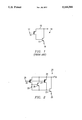
- FIG. 1 a typical prior art driver circuit 10 is shown in FIG. 1.
- the circuit 10 includes a high gain NPN output transistor 11 and a single p-channel FET 12 pre-driver.
- the NPN transistor 11 has its collector connected to a supply voltage on line 15, and its emitter connected to an output node 16, which is connected in operation to the desired load.
- the pre-driver p-channel FET 12 has its source connected to the supply voltage on line 15, and its drain connected to the base of the NPN transistor 11.
- the input to the circuit 10 is applied to the gate of the p-channel FET 12 from input node 17.
- the input signal has a step function waveform having a very rapid commutation, or falling edge time.
- the waveform of the output signal delivered to the load also has a rapid rise time, tracking the input waveform; however, the capacitive elements in the circuit, notably the capacitance of the base electrode of the NPN transistor 11, need to be charged before the NPN transistor 11 can be turned on.
- the single p-channel FET 12, on the other hand, can only supply a fixed amount of drive current to charge the base of the transistor 11, thereby defining the rate at which the transistor 11 can be turned on, or switched into conduction.
- a driver circuit in which a large current gain is available when needed during a slewing condition, but without increasing the total voltage drop of the driver when fully turned on. More particularly, and in accordance with a broad aspect of the invention, a driver circuit is provided which has a high output current and fast slew rate.
- the circuit includes a bipolar output transistor having an output for connection to a load, and a control element responsive to drive current signals to turn the bipolar output transistor on and off.
- a drive circuit controls the drive current signals to the bipolar output transistor during and after the turn-on of the bipolar output transistor, and a turn-on circuit supplies drive current to the control element of the bipolar transistor only to assist the bipolar output transistor turn-on.
- the drive circuit has a main drive current transistor connected to the control element of the bipolar output transistor, and has a control element connected to a driver circuit input node.
- the turn-on circuit has a turn-on drive current transistor with its current path connected in parallel with the main drive current transistor.
- the turn-on circuit also has a bias resistor connected to turn off the turn-on drive current transistor when the bipolar output transistor is turned on, whereby the turn-on drive current transistor does not drop voltage supplied by the circuit during turned on operation.
- the bipolar output transistor and the turn-on drive current transistor are bipolar NPN transistors, and the main drive current transistor and the input transistor are p-channel FET devices.
- the transistors therefore, can be fabricated in a single isolation well of an integrated circuit chip.
- a method for providing a high output current to a low impedance load includes the steps of providing a bipolar output transistor having an output for connection to a load, and a control element responsive to drive current signals to turn the bipolar output transistor on and off, controlling the drive current signals to the bipolar output transistor during and after the turn-on of the bipolar output transistor, and supplying an additional drive current to the control element of the bipolar transistor to assist the bipolar output transistor turn-on.
- FIG. 1 is an electrical schematic diagram of a power driver circuit, in accordance with the prior art.
- FIG. 2 is an electrical schematic diagram of a power driver circuit, in accordance with a preferred embodiment of the invention.
- a driver circuit 20, in accordance with a preferred embodiment of the invention is shown schematically in FIG. 2.
- the circuit includes a high current output driver NPN transistor 23, having its collector connected to a line 24 to which a supply voltage, V cc , is connected, and having its emitter connected to an output node 25 to which a load can be connected.
- the load (not shown) can be, for example, a low impedance load, and may include resistive, inductive, or capacitive elements, or some combination thereof.
- a p-channel FET 27 has its source connected to the supply voltage line 24 and its drain connected to the base of the NPN transistor 23. The gate of the p-channel FET 27 is connected to a driver circuit input node 28.
- the p-channel FET 27 serves as a main drive current transistor, providing a circuit to control the drive current signals to the output driver NPN transistor 23 both during and after its turn-on.
- the circuit described so far is similar to the circuit described above with regard to the prior art circuit of FIG. 1.
- a second NPN transistor 30, serving as a turn-on drive current transistor is connected in a Darlington configuration in conjunction with the first NPN transistor 23, having its collector connected to the voltage supply line 24, and its emitter connected to the base of the first NPN transistor 23.
- a second p-channel FET 32 is provided to serve as an input transistor.
- the second p-channel FET 32 is of standard configuration, and operates to boost the turn-on current to the second NPN transistor 30.
- the second FET 32 has its source connected to the voltage supply line 24, its drain connected to the base of the second NPN transistor 30, and its gate connected to the input node 28.
- a high value bias resistor 33 is connected between the base and emitter of the second NPN transistor 30.
- the second NPN transistor 30 and the second p-channel FET 32 serve as a turn-on circuit to provide additional current drive to the output NPN transistor 23 only during its turn-on.
- the circuit including the second NPN transistor 30 and the second FET 32 supplies a large turn-on current to rapidly turn-on the first NPN output driver transistor 23 in response to a rapidly decreasing input waveform, such as a step function, square wave, or the like.
- the second NPN transistor 30 provides a high current which charges the capacitance of the base of the output driver transistor 23, enabling its turn-on significantly faster than the prior art circuit above described.
- the bias voltage between the base and the emitter of the second NPN transistor 30 is reduced, turning off the second NPN transistor 30.
- the second NPN transistor 30, therefore, does not contribute any voltage drop to the output of the circuit 20, the only voltage drop being the V BE drop produced by the output driver NPN transistor 23 plus the voltage drop between the drain and source of the FET 27. Although the second FET 23 is not turned off, its effect on the circuit 20 is minimal due to the very high value of the resistor 33 in the source drain path of the second FET 32.
- the second NPN transistor 30 When the drive voltage produced by the circuit 20 is to be turned off, the second NPN transistor 30 has already been turned off. Thus, any capacitive discharge effects due to the existence of the second NPN transistor 30 in the circuit which may otherwise exist do not adversely affect the turn off time of the circuit.
- circuit embodiment illustrated employs only p-channel FET devices and NPN transistors, the circuit embodiment can easily be constructed in a single isolated integrated circuit well or tub, using standard BiCMOS technologies.
Priority Applications (4)
| Application Number | Priority Date | Filing Date | Title |
|---|---|---|---|
| US07/761,729 US5166544A (en) | 1991-09-18 | 1991-09-18 | Pseudo Darlington driver acts as Darlington during output slew, but has only 1 VBE drop when fully turned on |
| DE69228344T DE69228344T2 (de) | 1991-09-18 | 1992-08-20 | Treiberschaltung mit FET und bipolaren Transistoren |
| EP92307598A EP0533354B1 (fr) | 1991-09-18 | 1992-08-20 | Circuit d'attaque avec transistors FET et bipolaires |
| JP22298792A JP3278205B2 (ja) | 1991-09-18 | 1992-08-21 | ドライバ回路及び駆動方法 |
Applications Claiming Priority (1)
| Application Number | Priority Date | Filing Date | Title |
|---|---|---|---|
| US07/761,729 US5166544A (en) | 1991-09-18 | 1991-09-18 | Pseudo Darlington driver acts as Darlington during output slew, but has only 1 VBE drop when fully turned on |
Publications (1)
| Publication Number | Publication Date |
|---|---|
| US5166544A true US5166544A (en) | 1992-11-24 |
Family
ID=25063107
Family Applications (1)
| Application Number | Title | Priority Date | Filing Date |
|---|---|---|---|
| US07/761,729 Expired - Lifetime US5166544A (en) | 1991-09-18 | 1991-09-18 | Pseudo Darlington driver acts as Darlington during output slew, but has only 1 VBE drop when fully turned on |
Country Status (4)
| Country | Link |
|---|---|
| US (1) | US5166544A (fr) |
| EP (1) | EP0533354B1 (fr) |
| JP (1) | JP3278205B2 (fr) |
| DE (1) | DE69228344T2 (fr) |
Cited By (4)
| Publication number | Priority date | Publication date | Assignee | Title |
|---|---|---|---|---|
| US5450520A (en) * | 1991-08-16 | 1995-09-12 | Sgs-Thomson Microelectronics, Inc. | Load current sampling technique |
| US5510744A (en) * | 1993-05-24 | 1996-04-23 | Integrated Device Technology, Inc. | Control circuit for reducing ground and power bounce from an output driver circuit |
| US5550446A (en) * | 1994-09-30 | 1996-08-27 | Sgs-Thomson Microelectronics, Inc. | Dual slew rate circuit for driver transistors in disk drives |
| US20130099762A1 (en) * | 2011-10-20 | 2013-04-25 | Qualcomm Atheros, Inc. | Systems and methods for counteracting overvoltage events |
Citations (5)
| Publication number | Priority date | Publication date | Assignee | Title |
|---|---|---|---|---|
| JPS54148466A (en) * | 1978-05-15 | 1979-11-20 | Fuji Electric Co Ltd | Switching semiconductor device |
| US4590395A (en) * | 1984-07-20 | 1986-05-20 | Honeywell Inc. | FET-bipolar drive circuit |
| US4885486A (en) * | 1987-12-21 | 1989-12-05 | Sundstrand Corp. | Darlington amplifier with high speed turnoff |
| USRE33378E (en) * | 1983-10-14 | 1990-10-09 | Sundstrand Corporation | Incremental base drive circuit for a power transistor |
| US5045734A (en) * | 1990-06-08 | 1991-09-03 | Sundstrand Corporation | High power switch |
Family Cites Families (6)
| Publication number | Priority date | Publication date | Assignee | Title |
|---|---|---|---|---|
| JPH0783252B2 (ja) * | 1982-07-12 | 1995-09-06 | 株式会社日立製作所 | 半導体集積回路装置 |
| JPS625722A (ja) * | 1985-07-01 | 1987-01-12 | Toshiba Corp | インバ−タ回路 |
| DE3709383A1 (de) * | 1987-03-21 | 1988-09-29 | Licentia Gmbh | Einrichtung zur ansteuerung von transistorschaltern in darlington-anordnung |
| JPS6439817A (en) * | 1987-08-05 | 1989-02-10 | Toshiba Corp | Complementary output circuit |
| FR2638916B1 (fr) * | 1988-11-08 | 1994-04-01 | Bull Sa | Amplificateur binaire integre et circuit integre l'incorporant |
| JPH0799931B2 (ja) * | 1989-09-08 | 1995-10-25 | 東洋電機製造株式会社 | スイッチング素子の駆動回路 |
-
1991
- 1991-09-18 US US07/761,729 patent/US5166544A/en not_active Expired - Lifetime
-
1992
- 1992-08-20 EP EP92307598A patent/EP0533354B1/fr not_active Expired - Lifetime
- 1992-08-20 DE DE69228344T patent/DE69228344T2/de not_active Expired - Fee Related
- 1992-08-21 JP JP22298792A patent/JP3278205B2/ja not_active Expired - Fee Related
Patent Citations (5)
| Publication number | Priority date | Publication date | Assignee | Title |
|---|---|---|---|---|
| JPS54148466A (en) * | 1978-05-15 | 1979-11-20 | Fuji Electric Co Ltd | Switching semiconductor device |
| USRE33378E (en) * | 1983-10-14 | 1990-10-09 | Sundstrand Corporation | Incremental base drive circuit for a power transistor |
| US4590395A (en) * | 1984-07-20 | 1986-05-20 | Honeywell Inc. | FET-bipolar drive circuit |
| US4885486A (en) * | 1987-12-21 | 1989-12-05 | Sundstrand Corp. | Darlington amplifier with high speed turnoff |
| US5045734A (en) * | 1990-06-08 | 1991-09-03 | Sundstrand Corporation | High power switch |
Cited By (4)
| Publication number | Priority date | Publication date | Assignee | Title |
|---|---|---|---|---|
| US5450520A (en) * | 1991-08-16 | 1995-09-12 | Sgs-Thomson Microelectronics, Inc. | Load current sampling technique |
| US5510744A (en) * | 1993-05-24 | 1996-04-23 | Integrated Device Technology, Inc. | Control circuit for reducing ground and power bounce from an output driver circuit |
| US5550446A (en) * | 1994-09-30 | 1996-08-27 | Sgs-Thomson Microelectronics, Inc. | Dual slew rate circuit for driver transistors in disk drives |
| US20130099762A1 (en) * | 2011-10-20 | 2013-04-25 | Qualcomm Atheros, Inc. | Systems and methods for counteracting overvoltage events |
Also Published As
| Publication number | Publication date |
|---|---|
| EP0533354B1 (fr) | 1999-02-03 |
| EP0533354A1 (fr) | 1993-03-24 |
| JPH066196A (ja) | 1994-01-14 |
| DE69228344D1 (de) | 1999-03-18 |
| DE69228344T2 (de) | 1999-06-17 |
| JP3278205B2 (ja) | 2002-04-30 |
Similar Documents
| Publication | Publication Date | Title |
|---|---|---|
| US5742193A (en) | Driver circuit including preslewing circuit for improved slew rate control | |
| US5939909A (en) | Driver circuit having preslewing circuitry for improved slew rate control | |
| US5828245A (en) | Driver circuit including amplifier operated in a switching mode | |
| US5296765A (en) | Driver circuit for sinking current to two supply voltages | |
| US8310296B2 (en) | Driving transistor control circuit | |
| US5546043A (en) | Circuit arrangement for driving an MOS field-effect transistor | |
| US4471245A (en) | FET Gating circuit with fast turn-on capacitor | |
| US20040169973A1 (en) | Driver circuit connected to a switched capacitor and method of operating same | |
| JPH08293774A (ja) | ゲート駆動回路 | |
| WO1995031852A1 (fr) | Dispositif d'attaque de charge | |
| US20060044051A1 (en) | Bootstrap diode emulator with dynamic back-gate biasing and short-circuit protection | |
| US5436588A (en) | Click/pop free bias circuit | |
| JPH03185916A (ja) | パワーfet用適応ゲート充電回路 | |
| EP0427086B1 (fr) | Circuit de décharge de grille adaptative pour transistors à effet de champ de puissance | |
| US5432665A (en) | Short circuit protected capacitive load driver | |
| US5786709A (en) | Integrated circuit output driver incorporating power distribution noise suppression circuitry | |
| US5166544A (en) | Pseudo Darlington driver acts as Darlington during output slew, but has only 1 VBE drop when fully turned on | |
| US5038058A (en) | BiCMOS TTL output driver | |
| US5410190A (en) | Circuit for shortening the turn-off time of a power transistor | |
| US6522199B2 (en) | Reconfigurable dual-mode multiple stage operational amplifiers | |
| JPH03141720A (ja) | パワースイッチ回路 | |
| CN113785492B (zh) | 具有栅极电流重用的氮化镓激光二极管驱动场效晶体管 | |
| JP3258050B2 (ja) | 誘導性負荷用mosfetを備えた回路装置 | |
| JPH11234108A (ja) | 誘導負荷をスイッチングするためのスイッチング装置 | |
| US6940319B2 (en) | Device for controlling high and low levels of a voltage-controlled power switch |
Legal Events
| Date | Code | Title | Description |
|---|---|---|---|
| AS | Assignment |
Owner name: SGS-THOMSON MICROELECTRONICS, INC., TEXAS Free format text: ASSIGNMENT OF ASSIGNORS INTEREST.;ASSIGNOR:CAROBOLANTE, FRANCESCO;REEL/FRAME:005860/0895 Effective date: 19910909 |
|
| STCF | Information on status: patent grant |
Free format text: PATENTED CASE |
|
| FEPP | Fee payment procedure |
Free format text: PAYER NUMBER DE-ASSIGNED (ORIGINAL EVENT CODE: RMPN); ENTITY STATUS OF PATENT OWNER: LARGE ENTITY Free format text: PAYOR NUMBER ASSIGNED (ORIGINAL EVENT CODE: ASPN); ENTITY STATUS OF PATENT OWNER: LARGE ENTITY |
|
| FEPP | Fee payment procedure |
Free format text: PAYOR NUMBER ASSIGNED (ORIGINAL EVENT CODE: ASPN); ENTITY STATUS OF PATENT OWNER: LARGE ENTITY |
|
| FPAY | Fee payment |
Year of fee payment: 4 |
|
| FPAY | Fee payment |
Year of fee payment: 8 |
|
| FPAY | Fee payment |
Year of fee payment: 12 |