US4953117A - Method and apparatus for converting sampling frequencies - Google Patents
Method and apparatus for converting sampling frequencies Download PDFInfo
- Publication number
- US4953117A US4953117A US07/288,960 US28896088A US4953117A US 4953117 A US4953117 A US 4953117A US 28896088 A US28896088 A US 28896088A US 4953117 A US4953117 A US 4953117A
- Authority
- US
- United States
- Prior art keywords
- output
- sampling frequency
- input
- period
- data
- Prior art date
- Legal status (The legal status is an assumption and is not a legal conclusion. Google has not performed a legal analysis and makes no representation as to the accuracy of the status listed.)
- Expired - Lifetime
Links
Images
Classifications
-
- H—ELECTRICITY
- H03—ELECTRONIC CIRCUITRY
- H03H—IMPEDANCE NETWORKS, e.g. RESONANT CIRCUITS; RESONATORS
- H03H17/00—Networks using digital techniques
-
- H—ELECTRICITY
- H03—ELECTRONIC CIRCUITRY
- H03H—IMPEDANCE NETWORKS, e.g. RESONANT CIRCUITS; RESONATORS
- H03H17/00—Networks using digital techniques
- H03H17/02—Frequency selective networks
- H03H17/06—Non-recursive filters
- H03H17/0621—Non-recursive filters with input-sampling frequency and output-delivery frequency which differ, e.g. extrapolation; Anti-aliasing
- H03H17/0628—Non-recursive filters with input-sampling frequency and output-delivery frequency which differ, e.g. extrapolation; Anti-aliasing the input and output signals being derived from two separate clocks, i.e. asynchronous sample rate conversion
Definitions
- This invention relates to a sampling frequency converter for converting a sequence of input data samples having an input sampling frequency into a sequence of output data samples having a different output sampling frequency.
- the present invention finds particular use in, for example, converting between sampling frequencies associated with different PCM audio signal transmission systems.
- PCM signal transmission systems have been introduced, many of these using different sampling frequencies to digitize and transmit audio signals.
- the so-called compact disk system encodes an audio signal as a PCM signal recorded at a sampling frequency on the order of about 44.1kHz.
- a PCM processor is known in which an input audio signal is sampled at a frequency of 44.056kHz, this sampling frequency being used both to encode and decode a PCM audio signal.
- broadcast satellite systems are known to broadcast PCM audio signals in what has been designated the A mode at a sampling frequency of 32kHz and at what has been designated the B mode at a sampling frequency of 48kHz.
- these different PCM samples having different sampling frequencies are to be interchanged such that the PCM signal produced by one system is to be transmitted over a communications system which uses a different PCM sampling frequency, and this signal is to be used eventually by yet another system employing a still different sampling frequency.
- the ability to convert PCM signals in particular, and sampled data in general, from one sampling frequency to another is desirable.
- a relatively simple, straightforward sampling frequency converter relies upon digital-to-analog conversion of a PCM signal which, subsequently, is re-converted to yet another PCM signal at a desired sampling frequency. That is, the input PCM signal is converted to analog form and this converted signal then is sampled at the desired output sampling frequency in an analog-to-digital converter to derive the PCM signal with the desired output sampling frequency.
- Such DAC-ADC processing is relatively complicated and expensive and is subject to significant deterioration in signal quality.
- quantizing errors are introduced into each analog-to-digital conversion and these quantizing errors are cumulative when an input analog signal first is digitized, then converted to analog form and then re-digitized, all for the purpose of modifying the sampling frequency of the resultant PCM audio signal.
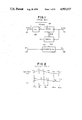
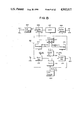
- FIG. 1 of the appended drawings Digital converters by which an input PCM signal is converted to a digital signal of desired sampling frequency, without requiring an intermediate analog conversion step, are known.
- FIG. 1 of the appended drawings One example is shown in FIG. 1 of the appended drawings and this figure relates to a sampling frequency converter disclosed in Japanese laid-open Patent Publications Nos. 57-115015 and 61-204700.
- the prior art sampling frequency converter shown in FIG. 1 is supplied with an input sampling clock signal Fs.sub.(in) having an input sampling frequency fs.sub.(in) and with an output sampling clock Fs.sub.(out) having an output sampling frequency fs.sub.(out).
- a sequence of input data samples x i with the input sampling frequency fs.sub.(in) is converted to a sequence of output data samples y j having the output sampling frequency fs.sub.(out).
- This high frequency clock signal is supplied to a counter 103 which is set in response to each pulse of the input sampling clock signal Fs.sub.(in) and is reset in response to each output sampling clock signal Fs.sub.(out).
- the output sampling clock signal is supplied to the reset input R of counter 103 and also to a latch input L of a N-bit register 105.
- the output of counter 103 also is coupled to register 105; and the count reached by the counter is transferred to and latched in the register upon the occurrence of an output sampling clock pulse.
- the count reached by counter 103 and latched in register 105 is representative of the phase of the output sampling clock pulse with respect to the immediately preceding input sampling clock pulse. That is, the phase difference between the output sampling point and the immediately preceding input sampling point is represented by the N-bit count which is normalized to unity. This N-bit normalized phase difference is supplied to a calculating circuit 106.
- Calculating circuit 106 functions to convert the input data samples x i to output data samples y j in response to each N-bit normalized phase difference supplied thereto by register 105.
- the converted output data samples are obtained at output terminal 108.
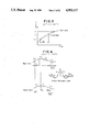
- phase data ⁇ j The relationship between the N-bit phase data stored in register 105 and represented as phase data ⁇ j , input data samples x i and output data samples y j are graphically depicted in FIG. 2.
- the resultant analog signal would, ideally, be identical to the analog representation of output data sample y j .
- Calculating circuit 106 functions to calculate the sample value of an output data sample y j at an output sampling point in response to an input data sample x i by using multinomial interpolation or digital filtering, as described below.
- the method of calculating an approximate value of an output data sample by multinomial interpolation is represented.
- the multinomial interpolation is interpolation of the first degree, commonly referred to as linear interpolation.
- samples x i and x i-1 represent amplitudes of the input data samples
- y j represents an amplitude of a data output sample
- ⁇ j represents the phase of an output sample point relative to the inmediately preceding input sample point (0 ⁇ j ⁇ 1).
- the amplitude of y j of the output sample point may be expressed as:
- the output amplitude at a desired output sample point may be calculated from the data input amplitudes x i and x i-1 and from the phase data ⁇ j .
- L-1 zero-valued samples are filled between adjacent samples of the input sampling sequence x i .
- the apparent sampling frequency is increased by a factor of L but the spectrum of the input sampling sequence remains unchanged.
- the sampling sequence with this increased sampling frequency then is convolved with (or multiplied by) a coefficient sequence K 0 , K 1 , K 2 , . . . , K r , . . . , K 2r-1 , K 2r which are samples of the impulse response of a low-pass filter having a pass band which passes the lower of the input sampling frequency fs.sub.(in) or the output sampling frequency fs.sub.(out) in a range up to L/2 times the passed sampling frequency.
- interpolated sample data having a sampling rate L times that of the input sampling frequency is obtained.
- the interpolated sample data y j ' whose sampling rate is L times the input rate may be represented as: ##EQU1##
- the Lth coefficients may be extracted and summed in a summation of products process that may be carried out by a digital signal processor (DSP)
- DSP digital signal processor
- the amplitude of the L-th output sample may be reduced by a factor 1/M, to produce an output data sample y j whose sampling frequency is converted to L/M relative to the input sampling frequency.
- Obtaining the output sampling sequence y j by the aforementioned convolution calculation generally relies upon a high speed clock signal which is generated by increasing the input sampling frequency (or the output sampling frequency) many times. This multiple of the input data sampling frequency (or output data sampling frequency) is used to drive the digital signal processor.
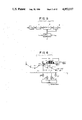
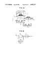
- FIGS. 5-7 Another prior art example of a sampling frequency converter is illustrated in FIGS. 5-7
- the input data sequence is over-sampled by a fixed ratio, for example by a factor of 4, and the oversampled input data sequence is supplied to a buffer circuit from which four data samples are read, each being multiplied by a coefficient related to the phase difference between the input sampling clock Fs1 and the output sampling clock Fs2.
- the products are summed, thereby producing the desired output data sequence at the selected output sampling frequency, with the resultant output samples each exhibiting proper amplitude values.
- input data having an input sampling rate of fs 1 is supplied to a two-stage fixed ratio over-sampling filter 1 and is converted into data whose sampling frequency is a multiple of the input sampling rate.
- the first stage of over-sampling filter 1 operates to increase the input sampling frequency by K 1 -times and, thus, may be considered a K 1 -times over-sampling filter.
- the second stage of filter 1 functions to increase the sampling rate of the samples supplied thereto from the first stage by a factor K 2 .
- the second stage of filter 1 may be considered a K 2 -times over-sampling filter.
- over-sampling filter 1 The output of over-sampling filter 1 is supplied to buffer 3. Within a period Ts1 of the input sampling clock Fs1, there are included four samples of the oversampled input data, and these four samples are read out from buffer 3 during the period Ts1.
- the buffer write-in and read-out operations are controlled by an output of clock processor 4.
- the four samples read from buffer 3 are multiplied by predetermined coefficients in a digital filter 2, the latter also being controlled by clock processor 4. As a result of this multiplication operation, output data samples having the desired sampling rate Fs2 are obtained.
- the instantaneous relative time difference dt i between the input sampling clock Fs1 and the output sampling clock Fs2, that is, between the input and output data samples, is detected by clock processor 4. Based upon this relative time difference dt i , buffer 3 and digital filter 2 are controlled in the manner described below.
- FIG. 6 is a waveform diagram useful in understanding the operation of digital filter 2.
- the oversampled input data samples are represented as samples x i , x i+1 , . . . , having a sampling rate 4fs1; and output data samples y i-1 , y i , . . . , exhibit the sampling rate of Fs2 and are produced at times relative to the oversampled samples x i , x i+1 , etc.
- the amplitude of an output sample y i is obtained by multiplying four oversampled samples x i+3 , x i+4 , x i+5 and x i+6 by coefficients c i , c j , c k and c l , respectively, and then adding all of these products together.
- the coefficients c i , c j , etc. are samples of the impulse response of a low pass filter, similar to that shown in FIG. 4, represented by, for example, 32K samples.
- coefficient samples are stored in a coefficient table C which is shifted so that its center coincides with the time at which output sample y i is produced Then, the coefficients c i , c j , c k and c l are selected from the coefficient table C at the times that oversampled data samples x i+3 , x i+4 , etc. are read from buffer 3.
- the relative time difference dt between an input data sample, assumed to be sample x i+3 , and output sample y i (the precise position where an output sample amplitude is to be calculated) cannot be measured accurately due to clock jitter or the like.
- a time-related error in determining the position of the output sample causes an amplitude error in the sample amplitude calculation.
- This amplitude error must be kept below one quantizing step. That is, the least significant bit in an output sample cannot be erroneous. Since the relative time difference dt cannot be measured, it must be calculated to an accuracy of virtually 16 bits.
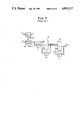
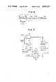
- FIG. 7 is a block diagram of one prior art example of clock processor 4 used to provide an error-free updating of relative time difference dt(i) carried out by measuring and averaging the output sampling period Ts2 and accumulating relative time differences dt.
- the embodiment of FIG. 7 includes a phase locked loop circuit 5, a counter 6, a random access memory (RAM) 7, adders 8 and 9 and delay circuits 10 and 11.
- Phase locked loop 5 generates a clock signal whose frequency is a multiple of the input sampling frequency fs1, that is, a clock frequency equal to 2 k fs1.
- This clock signal is used to measure the period Ts2 of the output sampling frequency fs2.
- This measured period is designated Ts2q(i) which is coarsely quantized with an accuracy of 6 to 7 bits.
- the measured output sampling period Ts2q(i) is averaged over a sufficiently long time period to increase its resolution to 16 bits (or more), and this averaged output sampling period is designated Ts2(est)(i).
- the average value Ts2(est)(i) must be measured such that no systematic down-rounding or up-rounding occurs over several samples because values due to such up-rounding or down-rounding accumulate as errors.
- a simple FIR averaging circuit for example, one with a z-Transform
- RAM 7, adder 8 and delay circuit 10 function as averaging circuitry, and the value Ts2(est)(i) is provided at the output of adder 8.
- calculation and control of the output data samples are carried out as a function of the relative time difference dt i , and this relative time difference dt i is determined from the input sampling clock Fs1 and the output sampling clock Fs2. That is, once the time difference dt i is calculated, it is used to generate the addresses for the filter coefficients which, in turn, are used to multiply the oversampled input data samples to calculate the output data samples.
- This technique suffers from several disadvantages: the overall calculating process is complex and time-consuming. Also, since the read/write operations of the buffer have been controlled as a function of the time difference dt i produced by clock processor 4 (FIG. 5), such read/write control has been complicated.
- Another object of this invention is to provide a method and apparatus for converging a signal sampling frequency without relying upon the time difference dt between input and output data samples.
- a further object of this invention is to provide a technique for generating addresses for selecting filter coefficients used for sampling frequency conversion which is of relatively simple yet accurate implementation.
- An additional object of this invention is to provide sampling frequency conversion that suffers from minimal quantization error.
- a sampling frequency converter for converting sampled input data having an input sampling frequency into sampled output data having a selected output sampling frequency.
- a relative ratio between periods of the input and output data samples is determined, and this determined ratio is averaged over a predetermined duration and used to generate filter coefficients which are used in a sampling filter circuit for converting the sampled input data into sampled output data.
- the sampling frequency of the sampled input data is increased by an over-sampling circuit, and the oversampled data is temporarily stored and subsequently read at a rate determined by the ratio between periods of the input and output sampling frequencies.
- the input sampling frequency periods as well as the output sampling frequency periods each are averaged; and both averaged periods are used to generate filter coefficients which are supplied to a variable filter that produces converted data samples by processing the oversampled data read from the buffer with the filter coefficients.
- converted data samples of the output sampling frequency are generated.
- FIG. 1 is a block diagram, described above, showing a prior art sampling frequency converter
- FIGS. 2-4 described above, are diagrams which are useful in understanding the operation of the prior art sampling frequency converter
- FIG. 5, described above, is a block diagram of another prior art sampling frequency converter
- FIG. 6, described above, is a diagram useful in understanding the operation of the sampling frequency converter of FIG. 5;
- FIG. 7, described above, is a block diagram of one embodiment of the clock processor used in the sampling frequency converter of FIG. 5;
- FIG. 8 is a block diagram of one embodiment of a sampling frequency converter clock processor in accordance with the present invention.
- FIG. 9 is a block diagram of overflow check circuit 12 shown in FIG. 8;
- FIG. 10 is a waveform diagram useful in understanding the operation of the embodiment shown in FIG. 9;
- FIG. 11 is a block diagram of another embodiment of the overflow check circuit shown in FIG. 8;
- FIG. 12 is a waveform diagram useful in understanding the operation of the embodiment shown in FIG. 11;
- FIG. 13 is a block diagram of another embodiment of a sampling frequency converter in accordance with the present invention.
- FIG. 14 is a waveform diagram useful in understanding the operation of the embodiment shown in FIG. 13;
- FIG. 15 is a block diagram of an event detector shown in FIG. 13;
- FIG. 16 is a diagram useful in understanding the operation of the event detector shown in FIG. 15;
- FIG. 17 is a block diagram of one embodiment of averaging circuit 215 shown in FIG. 13.
- FIG. 18 is a diagram useful in understanding the operation of the averaging circuit shown in FIG. 17.
- the first coefficient c i of the four coefficients c i , c j , c k and c l is stored at an address A 1 of the coefficient table C.
- This address A 1 is related to the relative time difference dt(i) between input data sample x i+3 and the time of occurrence of output data sample y i as follows:
- address A 1 is a positive quantity and always is less than 0.25. Accordingly, a more general formula for address A 1 is:
- a 1 is the complement of dt(i) Mod Ts1; and the calculation of dt(i), as was done in the aforementioned prior art, can be replaced by the direct calculation of address A 1 .
- the other addresses of the coefficient table, sometimes referred to herein as filter addresses, are:
- this embodiment differs from the prior art shown in FIG. 7 in that the coefficient address as well as the buffer control are obtained directly from the averaged output sampling period Ts2(est)(i), produced at the output of adder 8.
- the prior art used the averaged output sampling period Ts2(est)(i) to calculate the relative time difference dt(i) which then was used to generate addresses A i
- the present invention avoids the complex and time-consuming steps needed in the calculation of dt(i).
- FIG. 8 Those elements shown in FIG. 8 which are the same as those described above in conjunction with FIG. 7 are identified by the same reference numerals. Further description of these previously described elements is not provided. From FIG. 8, it is seen that the output of adder 8 is coupled to an adder 18 which calculates the coefficient address used to read out the appropriate filter coefficient which, in turn, is used to multiply the input data sample to effect a sampling frequency conversion. The coefficient address is fed back to adder 18 by way of a delay circuit 11. The adder output also is supplied to an overflow check circuit 12 which selectively couples a fixed value to adder 18 for summation with the other inputs supplied to this adder, depending upon the presence or absence of a detected overflow.
- sampling frequency conversion operation may increase the input sampling frequency, referred to herein as an "up convert”, or it may decrease the input sampling frequency, referred to as a “down convert”.
- up convert the input sampling frequency
- down convert the input sampling frequency
- overflow check circuit 12 used to carry out an up convert includes a comparator 14 which compares the coefficient address A i produced by adder 18 with the averaged output sampling period Ts2(est)(i) generated by adder 8 (FIG. 8). When the coefficient address A i is less than the averaged output sampling period Ts2(est)(i), the constant value 0.25 is added to the coefficient address so as to generate the next coefficient address. Conversely, when coefficient address A i is greater than the averaged output sampling period Ts2(est)(i), the constant value 0.25 is not added to the coefficient address. Thus, depending upon the output of comparator 14, the constant numerical value 0.25 is selectively supplied to adder 18 through a gate circuit 13 having an enable input coupled to the comparator.
- coefficient addresses A 1 , A 2 and A 3 will not be larger than the averaged output sampling period Ts2(est)(i), but coefficient address A 4 possibly may be larger than the averaged output sampling period Ts2(est)(i).
- the averaged output sampling period Ts2(est)(i) is supplied to the adder to be subtracted from the other values then supplied thereto.
- the averaged output sampling period Ts2(est)(i) is not supplied to adder 18 at the time that addresses A 1 , A 2 and A 3 are generated.
- input sampling period Ts1 is normalized to unity, resulting in the averaged output sampling period Ts2(est)(i) becoming approximately 0.9.
- input data samples x 1 , x 2 , . . . represent the oversampled input data samples and the output data samples are represented as y i , y i+1 , y i+2 , etc.
- the amplitudes of these three consecutive output data samples are to be calculated to effect proper frequency conversion.
- the relative times of occurrences of the output data samples and the oversampled input data samples are as illustrated.
- the low pass filter impulse response of period Ts1 is seen to be shifted so as to be centered at each output data sample.
- the amplitude of the impulse response at the time of occurrence of each oversampled input data sample is the filter coefficient with which that input data sample is multiplied. Closely spaced samples of the impulse response amplitude are stored in an addressable memory; and the address used to read out a respective sample is generated by adder 18.
- the address of the coefficient to be multiplied by the oversampled input data sample x i is assumed to be 0.1. Then, the addresses of the coefficients to be multiplied by the subsequent oversampled input data samples x 2 x 3 and x 4 become:
- each of coefficient addresses A 1 to A 4 is less than the averaged output sampling period Ts2(est)(i) which has been defined as 0.9.
- comparator 14 determines that each of these addresses A i is smaller than the averaged output sampling period Ts2(est)(i) and activates gate 13.
- the coefficient A 4 and the constant value 0.25 are supplied as positive values to adder 18, while the averaged output sampling period Ts2(est)(i) is supplied as a negative value to the adder.
- address A 1 of the first coefficient for calculating the next output data sample y i+1 that is, address A 1 of the coefficient to be multiplied by the next oversampled input data sample x 5 becomes: ##EQU2##
- addresses A 2 , A 3 and A 4 of the coefficients to be multiplied by the subsequent oversampled input data samples x 6 , x 7 and x 8 become:
- the address A 4 of the coefficient to be multiplied by the oversampled input data sample x 8 has been calculated as 0.95 and is larger than the averaged output sampling period Ts2(est)(i) which has been assumed to be 0.9.
- comparator 14 functions to disable gate 13.
- the value 0.25 is not added to the previous coefficient address A 4 . Rather, only the averaged output sampling period Ts2(est)(i) is subtracted from coefficient address A 4 .
- the oversampled input data sample to be multiplied by the coefficient stored at address A 1 is not the next sample x 9 but, rather, input data sample x 8 is used once again.
- address A 1 of the coefficient to be multiplied by the oversampled input data sample x 8 for calculating the output sample y i+2 becomes: ##EQU3##
- the output of comparator 14 indicates whether an oversampled input data sample is to be used again and, thus, the comparator output is used to control the read/write operation of buffer 3 shown in FIG. 5.
- overflow check circuit 12 will be described for the arrangement wherein a down convert in the sampling frequency is to be carried out. For example, let it be assumed that the output sampling period Ts2 is increased to be equal to 1.1 times the input sampling period Ts1. That is, the sampling frequency is reduced by a factor 10/11. To carry out this down convert, overflow check circuit 12 is configured as shown in FIG. 11. Here, a subtractor 16 functions to subtract the fixed constant value 0.25 from the averaged output sampling period Ts2(est)(i) to obtain a value which, along with a constant value 0.75, is compared in a comparator 15 to the coefficient address A i produced by adder 18.
- Comparator 15 is coupled to a selector 17 to control the operation of the selector for supplying to adder 18 either a constant value of 0.25 or a constant value of 0.5. More particularly, selector 17 responds to the output of comparator 15 to select the constant value 0.5 when coefficient address A i is:
- Selector 17 also responds to the output of comparator 15 to supply to adder 18 the constant value 0.25 when the coefficient address A i is determined to be:
- the constant value selected by selector 17 is added to the coefficient address A i by adder 18.
- the coefficient addresses A 1 , A 2 and A 3 each exhibit a value less than 0.75.
- selector 17 selects the constant value 0.25 to be added to the preceding coefficient address which is fed back to adder 18 by delay circuit 11.
- FIG. 12 illustrates waveforms similar to those shown in FIG. 10 and juxtaposes those waveforms with respect to oversampled input data samples x 1 , x 2 , etc. As was described previously in conjunction with FIG. 10, the illustrated impulse response characteristic is centered with respect to the time at which each output sample is to be produced.
- coefficient address A 4 falls within the range 0.75 ⁇ A 4 ⁇ 0.85 and comparator 15 controls selector 17 to select the constant value 0.5.
- the address A 1 of the coefficient to be multiplied by the next oversampled input data sample for calculating output data sample y i+1 becomes ##EQU4##
- Addresses A 2 , A 3 , A 4 of the coefficients to be multiplied by the subsequent oversampled input data samples x 7 , x 8 , x 9 are:
- coefficient address A 4 is:
- comparator 15 determines whether an oversampled input data sample is to be skipped.
- comparator 15 like comparator 14 of FIG. 9, is used for controlling the read/write operations of buffer 3 (FIG. 5).
- FIGS. 8-12 calculates the averaged output sampling period Ts2(est)(i) by using a high seed clock produced by increasing the input data sampling frequency fs1 (or, alternatively, the output data sampling frequency fs2) many times over, that is, by a factor 2 k .
- the sampling frequency converter of this embodiment has employed a PLL circuit operating at a high speed for generating that clock signal, and the PLL circuit requires a sufficiently wide capture range to follow the variations in frequency of the sampling clock signal Fs1 or Fs2 which it multiplies. Further, it may be difficult to synchronize the DSP which calculates the approximate values of the output data samples because the DSP operates in response to the high speed clock signal generated by the PLL.
- the averaging process for determining the averaged output sampling period Ts2(est)(i) to improve accuracy in the sampling rate conversion is carried out in a so-called open-loop calculation or averaging method based on the z-Transform ##EQU6## Using this averaging method, if a step form phase error occurs, a control error is produced.
- a signal input terminal 201 is supplied with the input data samples (x i ) to be converted, and a clock signal input terminal 202 is supplied with an input sampling clock signal Fs1 of the input data sampling frequency fs1.
- a clock signal input terminal 203 is supplied with an output sampling clock signal Fs2 having the sampling frequency fs2 of the output data samples (y j ) which are produced at a signal output terminal 204.
- a buffer memory 206 is coupled to oversampling circuit 205 for temporarily storing sample values [x i ]' of the oversampled input data samples having the sampling frequency 4.fs1.
- Digital signal processor (DSP) 207 is coupled to buffer 206 for subjecting the oversampled sequence [x i ]' read out from the buffer to a digital filtering process using filter coefficients which are samples of the impulse response of a low-pass filter capable of passing the increased sampling frequency 4.fs1 to thereby calculate an interpolated amplitude value at a sample point of the output data sample (y j ) whose sampling frequency thus has been converted to the output sampling frequency fs2.
- Another buffer memory 208 is coupled to DSP 207 for temporarily storing each of the interpolated amplitude values of the output data samples (y j ).
- a local clock generator 209 generates a local clock signal Fc to provide a source of timing signals for buffer memories 206, 208 and digital signal processor 207.
- a conversion controller 210 is adapted to control the operations of buffer memories 206, 208 and digital signal processor 207 in response to the sampling frequencies fs1, fs2 derived from sampling clock signals Fs1, Fs2 supplied to clock signal input terminals 202, 203 and to the local clock frequency fc derived from the local clock signal Fc.
- Digital signal processor 207 reads out filter coefficients (of the type described above) from a coefficient memory (not shown) according to coefficient addresses supplied by a coefficient address generator 217 of conversion controller 210 and performs a multiply-and-add operation with these filter coefficients.
- the digital signal processor in response to the oversampled sequence [x i ]' read from buffer memory 206, reads out four filter coefficients c i , c j , c k and c l which coincide in time to the sample points of the samples x i , x j , x k and x 1 , respectively, as schematically shown in FIG. 14.
- coefficients are included in a set of 2 k filter coefficients which constitute the impulse response characteristic of a low-pass filter to the sampling frequency 4.fs1.
- This set of coefficients is stored in, for example, a table, with the center address Ac of the coefficient filter set maintained coincident with a sample point t j of the output data sample sequence [y j ].
- the four samples x i , x j , x k , x l read from buffer 206 are multiplied by the filter coefficients c i , c j , c k , c l , respectively, and the products are summed, thereby calculating the interpolated output sample value y j at the sample point t j .
- Local clock generator 209 includes a quartz oscillator or the like oscillating at the local clock frequency fc.
- fc K.fo, where the factor K represents an integer that is a power of 2, such as 2N, and the frequency of represents a frequency higher than the input sampling frequency fs1 and higher than the output sampling frequency fs2.
- the sampling frequencies fs1, fs2 are generally close to 48kHz or below, and the frequency of also is selected close to 48kHz.
- the local clock frequency fc is of a frequency for which the DSP electronic circuitry (e. g. a DSP chip) constituting digital signal processor 207 is designed, and at this frequency, the digital filtering process in the digital signal processor is performed such that the quantization error of the output data samples (y j ) is kept below one quantizing step.
- a timing generator 214 is included in controller 210 for generating various timing signals in response to the modulo-K count output; and first and second averaging circuits 215, 216 are used in the controller for calculating estimated sampling periods Ts est 1/To, Ts est 2/To of the input and output sampling clock signals Fs1, Fs2, respectively, based upon the relative time differences dt q1 /To, dt q2 /To measured by event detectors 212, 213.
- the conversion controller also includes a coefficient address generator 217 for calculating the coefficient addresses in response to the estimated sampling periods Ts est 1/To, Ts est 2/To obtained by averaging circuits 215, 216, for selecting the approximate filter coefficients with which to multiply the samples read from buffer 206.
- Event detectors 212, 213 are adapted to measure the relative time differences dt q1 , dt q2 between each of the sampling periods Ts1, Ts2 and the clock period To, but such time differences cannot be measured in real time with high accuracy due to clock jitter or the like.
- clock edges or sync patterns for the sampling clock signals Fs1 and Fs2 are detected during every clock period To, it being recognized that To is shorter than either of the sampling periods Ts1 and Ts2.
- event detector 212 a functional representation of event detector 212 is shown. It will be appreciated that this block diagram also is representative of event detector 213. For convenience, the following description is referenced to event detector 212.
- An adder 221 supplied with information representing the input sampling period Ts1 adds this input sampling period information to information representing the relative time difference dt.sub.(-1) of the preceding input sampling period Ts1 temporarily stored in register 222.
- the output of adder 221 thus is indicative of the relative time difference dt between the input sampling period Ts1 and the clock period To.
- This relative time difference information dt is fed back for storage in register 222 and also is supplied to a quantizing circuit 223.
- the quantizing circuit as shown in FIG.
- Averaging circuits 215, 216 supplied with signals representing the measured relative time differences dt q 1/To and dt q 2/To obtained from event detectors 212 and 213, respectively, estimate the input and output sampling periods Ts est 1/To and Ts est 2/To. These estimated sampling periods represent the ratio of the input sampling period Ts1 to clock period To and the ratio of the output sampling period Ts2 to clock period To.
- averaging circuit 215 is illustrated as including an adder 251, supplied with a representation of the measured relative time difference dt q /To between the input sampling period and the clock period To and subtracts therefrom information representing an estimated relative time difference dt est /To supplied thereto from an adder 252.
- Adder 251 calculates an error between the measured time difference dt q /To and the estimated relative time difference dt est /To. This error is monitored in an error monitor 253 coupled to adder 251. Correcting information ⁇ (Ts/To) for the next estimated input sample position, as shown in FIG. 18, is produced by a calculating circuit 254 based on the monitored error information, and this correcting information is supplied to a further adder 255.
- Adder 255 adds the correcting information ⁇ (Ts1/To) to information representing the previous estimated input sampling period (Ts est 1/To).sub.(-1) fed back through a register 256 and thereby calculates an estimated input sampling period Ts est 1/To.
- This estimated input sampling period is supplied to adder 252.
- register 256 is supplied at the start with information of an initial value Ts q0 of the estimated input sampling period from adder 255.
- adder 252 adds information representing the estimated input sampling period Ts est 1/To to information representing the previous estimated input sampling period (Ts est 1/To).sub.(-1) fed back through a register 257 and thereby calculates the estimated relative time difference dt est /To. This calculated information is supplied to adder 251. Register 257 is supplied at the start with an initial value dt q0 of the estimated relative time difference from adder 252.
- Information on the initial values Ts q0 and dt q0 supplied to registers 256 and 257 are obtained by direct quantized measurement of, for example, the relative time difference dt q .
- the estimated relative time difference falls within the observed range of the measured relative time difference dt q for long durations. Correction of the estimated input sampling period with the correcting information ⁇ (Ts1/To) avoids excessive changes to the estimated input sampling period Ts est /To and, thus, phase inversion and distortion are not produced.
- FIG. 17 is illustrative of a functional block diagram of averaging circuit 215, it will be appreciated that FIG. 17 also is representative of averaging circuit 216. Therefore, the foregoing description is applicable to averaging circuit 216.
- Event detector 212 detects where the measured relative time difference dt est occurs compared to the estimated relative time difference dt q .
- the history of this event is useful in calculating suitable corrections to the estimated input sampling period Ts est /To. If, for example, it took 500 samples for the estimated input relative time difference dt est with a constant estimated input sampling period Ts est 1 to change from a value below the measured relative time difference dt q range to a value above that range, then the current error in the estimated input sampling period Ts est 1 is estimated as 1/500 of the quantization step for the measured relative time difference dt q .
- Coefficient address generator 217 is supplied with information representing the estimated input sampling period Ts est 1/To provided by averaging circuit 215 with information representing the estimated output sampling period Ts est 2/To provided by averaging circuit 216 to generate from the ratio of the estimated output sampling period to the estimated input sampling period the coefficient addresses for reading out the filter coefficients c i , c j , c k , c l for use by digital signal processor 207 for interpolation processing.
- coefficient address generator 217 For an embodiment of coefficient address generator 217, reference may be made to FIGS. 8, 9 and 11.
Landscapes
- Physics & Mathematics (AREA)
- Engineering & Computer Science (AREA)
- Computer Hardware Design (AREA)
- Mathematical Physics (AREA)
- Transmission Systems Not Characterized By The Medium Used For Transmission (AREA)
- Compression, Expansion, Code Conversion, And Decoders (AREA)
- Complex Calculations (AREA)
- Stabilization Of Oscillater, Synchronisation, Frequency Synthesizers (AREA)
Applications Claiming Priority (2)
| Application Number | Priority Date | Filing Date | Title |
|---|---|---|---|
| JP62-332395 | 1987-12-29 | ||
| JP62332395A JP2600236B2 (ja) | 1987-12-29 | 1987-12-29 | サンプリング周波数変換回路 |
Publications (1)
| Publication Number | Publication Date |
|---|---|
| US4953117A true US4953117A (en) | 1990-08-28 |
Family
ID=18254491
Family Applications (1)
| Application Number | Title | Priority Date | Filing Date |
|---|---|---|---|
| US07/288,960 Expired - Lifetime US4953117A (en) | 1987-12-29 | 1988-12-23 | Method and apparatus for converting sampling frequencies |
Country Status (5)
| Country | Link |
|---|---|
| US (1) | US4953117A (de) |
| EP (2) | EP0599817B1 (de) |
| JP (1) | JP2600236B2 (de) |
| KR (1) | KR890011206A (de) |
| DE (2) | DE3856142T2 (de) |
Cited By (36)
| Publication number | Priority date | Publication date | Assignee | Title |
|---|---|---|---|---|
| US5365468A (en) * | 1992-02-17 | 1994-11-15 | Yamaha Corporation | Sampling frequency converter |
| US5383144A (en) * | 1990-11-20 | 1995-01-17 | Matsushita Electric Industrial Co., Ltd. | Subsampling method and interpolation method of digital signals |
| US5398029A (en) * | 1992-12-21 | 1995-03-14 | Nippon Precision Circuits Inc. | Sampling rate converter |
| US5463569A (en) * | 1994-06-24 | 1995-10-31 | General Electric Company | Decimation filter using a zero-fill circuit for providing a selectable decimation ratio |
| US5471411A (en) * | 1992-09-30 | 1995-11-28 | Analog Devices, Inc. | Interpolation filter with reduced set of filter coefficients |
| US5481267A (en) * | 1993-01-07 | 1996-01-02 | Nippon Precision Circuits Inc. | Sampling rate converter |
| US5485152A (en) * | 1993-09-13 | 1996-01-16 | Analog Devices, Inc. | Analog to digital conversion using non-uniform sample rates |
| US5489903A (en) * | 1993-09-13 | 1996-02-06 | Analog Devices, Inc. | Digital to analog conversion using non-uniform sample rates |
| US5512897A (en) * | 1995-03-15 | 1996-04-30 | Analog Devices, Inc. | Variable sample rate DAC |
| US5528240A (en) * | 1993-09-13 | 1996-06-18 | Analog Devices, Inc. | Digital phase-locked loop utilizing a high order sigma-delta modulator |
| US5548540A (en) * | 1994-06-24 | 1996-08-20 | General Electric Company | Decimation filter having a selectable decimation ratio |
| US5574454A (en) * | 1993-09-13 | 1996-11-12 | Analog Devices, Inc. | Digital phase-locked loop utilizing a high order sigma-delta modulator |
| US5585794A (en) * | 1991-12-13 | 1996-12-17 | Sgs-Thomson Microelectronics, S.R.L. | Electronic device for the automatic conversion of sampled frequencies |
| US5619202A (en) * | 1994-11-22 | 1997-04-08 | Analog Devices, Inc. | Variable sample rate ADC |
| JP2600236B2 (ja) | 1987-12-29 | 1997-04-16 | ソニー株式会社 | サンプリング周波数変換回路 |
| US5638010A (en) * | 1995-06-07 | 1997-06-10 | Analog Devices, Inc. | Digitally controlled oscillator for a phase-locked loop providing a residue signal for use in continuously variable interpolation and decimation filters |
| WO1997041552A1 (en) * | 1996-04-30 | 1997-11-06 | Quantum Corporation | Method and apparatus for spectral analysis in a disk recording system |
| US5712635A (en) * | 1993-09-13 | 1998-01-27 | Analog Devices Inc | Digital to analog conversion using nonuniform sample rates |
| US5721689A (en) * | 1995-12-18 | 1998-02-24 | Abb Power T&D Company Inc. | System and method for phasor estimation and frequency tracking in digital protection systems |
| US5732002A (en) * | 1995-05-23 | 1998-03-24 | Analog Devices, Inc. | Multi-rate IIR decimation and interpolation filters |
| US5787496A (en) * | 1995-04-28 | 1998-07-28 | Sony Corporation | Digital signal processor having a partitioned memory with first and second address areas for receiving and storing data in sychronism with first and second sampling clocks |
| US5832413A (en) * | 1995-12-18 | 1998-11-03 | Abb Power T&D Company Inc. | Generator protection system and method for phasor estimation and frequency tracking during frequency ramping |
| US5892468A (en) * | 1993-09-13 | 1999-04-06 | Analog Devices, Inc. | Digital-to-digital conversion using nonuniform sample rates |
| US5963160A (en) * | 1993-09-13 | 1999-10-05 | Analog Devices, Inc. | Analog to digital conversion using nonuniform sample rates |
| US5996044A (en) * | 1994-01-26 | 1999-11-30 | Sony Corporation | Sampling frequency converting device and memory address control device |
| US6016327A (en) * | 1997-10-03 | 2000-01-18 | At&T Corporation | Electronic memory system and method for use in system for reducing quantization noise |
| US6185482B1 (en) | 1998-03-10 | 2001-02-06 | Abb Power T&D Company Inc. | System and method for rms overcurrent backup function |
| US6278741B1 (en) * | 1999-10-22 | 2001-08-21 | Wideband Computers, Inc. | Timing recovery circuit in QAM modems |
| DE10106403A1 (de) * | 2001-02-12 | 2002-09-12 | Rohde & Schwarz | Vorrichtung und Verfahren zur Abtastratenumsetzung |
| US20030107508A1 (en) * | 2001-03-07 | 2003-06-12 | Yukio Koyanagi | Interpolating function generating apparatus and method, digital-analog converter, data interpolator, program, and record medium |
| US20050143981A1 (en) * | 2000-06-06 | 2005-06-30 | Yukio Koyanagi | Compressing method and apparatus, expanding method and apparatus, compression and expansion system, recorded medium, program |
| WO2015126956A1 (en) * | 2014-02-21 | 2015-08-27 | Summit Semiconductor, Llc | Synchronization of audio channel timing |
| EP2924879A4 (de) * | 2012-11-22 | 2016-08-24 | Ntt Electronics Corp | Vorrichtung zur abtastratenkonvertierung |
| US10582461B2 (en) | 2014-02-21 | 2020-03-03 | Summit Wireless Technologies, Inc. | Software based audio timing and synchronization |
| US10602468B2 (en) | 2014-02-21 | 2020-03-24 | Summit Wireless Technologies, Inc. | Software based audio timing and synchronization |
| CN112859616A (zh) * | 2021-01-27 | 2021-05-28 | 顺德职业技术学院 | 一种传感器采样间隔模糊控制器 |
Families Citing this family (11)
| Publication number | Priority date | Publication date | Assignee | Title |
|---|---|---|---|---|
| GB2236452B (en) * | 1989-07-14 | 1993-12-08 | Tektronix Inc | Coefficient reduction in a low ratio sampling rate converter |
| GB2242800B (en) * | 1990-04-03 | 1993-11-24 | Sony Corp | Digital phase detector arrangements |
| GB9301704D0 (en) * | 1993-01-28 | 1993-03-17 | Signal Processors Ltd | New digital modem design techniques |
| JPH07235861A (ja) * | 1993-12-08 | 1995-09-05 | Nokia Mobile Phones Ltd | 加重平均を使用したサンプリング周波数変換方法 |
| US6061704A (en) * | 1997-12-23 | 2000-05-09 | Telefonaktiebolaget Lm Ericsson | Method and apparatus for rate conversion |
| EP1458097A1 (de) * | 2003-03-11 | 2004-09-15 | Sony International (Europe) GmbH | Beliebige Abtastratenkonversion |
| JP4420092B2 (ja) * | 2007-09-18 | 2010-02-24 | ヤマハ株式会社 | 周波数判別回路およびサンプリング周波数変換装置 |
| GB2456360B (en) | 2008-10-13 | 2009-12-02 | Wolfson Microelectronics Plc | Sample rate converter |
| GB2464169B (en) * | 2008-10-13 | 2010-12-15 | Wolfson Microelectronics Plc | Sample rate converter |
| JP2012160907A (ja) * | 2011-01-31 | 2012-08-23 | Icom Inc | デジタルフィルタ、無線装置、フィルタリング方法及びプログラム |
| JP5573901B2 (ja) * | 2012-08-23 | 2014-08-20 | Nttエレクトロニクス株式会社 | 標本化レート変換装置 |
Citations (6)
| Publication number | Priority date | Publication date | Assignee | Title |
|---|---|---|---|---|
| US4020332A (en) * | 1975-09-24 | 1977-04-26 | Bell Telephone Laboratories, Incorporated | Interpolation-decimation circuit for increasing or decreasing digital sampling frequency |
| JPS57115015A (en) * | 1980-11-26 | 1982-07-17 | Biri Shiyutouudaa | Method and device for converting input sampled sequence into output sampled sequence |
| US4460890A (en) * | 1982-01-21 | 1984-07-17 | Sony Corporation | Direct digital to digital sampling rate conversion, method and apparatus |
| US4472785A (en) * | 1980-10-13 | 1984-09-18 | Victor Company Of Japan, Ltd. | Sampling frequency converter |
| JPS61204700A (ja) * | 1985-03-07 | 1986-09-10 | ソニー株式会社 | サンプリング周波数変換装置 |
| JPS62101112A (ja) * | 1985-10-28 | 1987-05-11 | Sony Corp | サンプリング周波数変換回路 |
Family Cites Families (4)
| Publication number | Priority date | Publication date | Assignee | Title |
|---|---|---|---|---|
| EP0084592B1 (de) * | 1982-01-26 | 1986-04-30 | WILLI STUDER AG Fabrik für elektronische Apparate | Verfahren und Schaltungsanordnung zur Messung der Zeitdifferenz zwischen Abtastzeitpunkten zweier abgetasteter Signale, insbesondere EIn- und Ausgangssignale eines Abtastratenumsetzers |
| ATE41840T1 (de) | 1983-10-06 | 1989-04-15 | Studer Willi Ag | Verfahren und vorrichtung zur umsetzung einer eingangsabtastfolge in eine ausgangsabtastfolge. |
| JPS60101112A (ja) * | 1983-11-07 | 1985-06-05 | Hitachi Chem Co Ltd | 熱硬化性樹脂組成物 |
| JP2600236B2 (ja) | 1987-12-29 | 1997-04-16 | ソニー株式会社 | サンプリング周波数変換回路 |
-
1987
- 1987-12-29 JP JP62332395A patent/JP2600236B2/ja not_active Expired - Fee Related
-
1988
- 1988-12-23 DE DE3856142T patent/DE3856142T2/de not_active Expired - Fee Related
- 1988-12-23 DE DE3853669T patent/DE3853669T2/de not_active Expired - Fee Related
- 1988-12-23 US US07/288,960 patent/US4953117A/en not_active Expired - Lifetime
- 1988-12-23 EP EP94101859A patent/EP0599817B1/de not_active Expired - Lifetime
- 1988-12-23 EP EP88312325A patent/EP0323200B1/de not_active Expired - Lifetime
- 1988-12-28 KR KR1019880017617A patent/KR890011206A/ko not_active Application Discontinuation
Patent Citations (6)
| Publication number | Priority date | Publication date | Assignee | Title |
|---|---|---|---|---|
| US4020332A (en) * | 1975-09-24 | 1977-04-26 | Bell Telephone Laboratories, Incorporated | Interpolation-decimation circuit for increasing or decreasing digital sampling frequency |
| US4472785A (en) * | 1980-10-13 | 1984-09-18 | Victor Company Of Japan, Ltd. | Sampling frequency converter |
| JPS57115015A (en) * | 1980-11-26 | 1982-07-17 | Biri Shiyutouudaa | Method and device for converting input sampled sequence into output sampled sequence |
| US4460890A (en) * | 1982-01-21 | 1984-07-17 | Sony Corporation | Direct digital to digital sampling rate conversion, method and apparatus |
| JPS61204700A (ja) * | 1985-03-07 | 1986-09-10 | ソニー株式会社 | サンプリング周波数変換装置 |
| JPS62101112A (ja) * | 1985-10-28 | 1987-05-11 | Sony Corp | サンプリング周波数変換回路 |
Cited By (47)
| Publication number | Priority date | Publication date | Assignee | Title |
|---|---|---|---|---|
| JP2600236B2 (ja) | 1987-12-29 | 1997-04-16 | ソニー株式会社 | サンプリング周波数変換回路 |
| US5383144A (en) * | 1990-11-20 | 1995-01-17 | Matsushita Electric Industrial Co., Ltd. | Subsampling method and interpolation method of digital signals |
| US5585794A (en) * | 1991-12-13 | 1996-12-17 | Sgs-Thomson Microelectronics, S.R.L. | Electronic device for the automatic conversion of sampled frequencies |
| US5365468A (en) * | 1992-02-17 | 1994-11-15 | Yamaha Corporation | Sampling frequency converter |
| US5471411A (en) * | 1992-09-30 | 1995-11-28 | Analog Devices, Inc. | Interpolation filter with reduced set of filter coefficients |
| US6141671A (en) * | 1992-09-30 | 2000-10-31 | Analog Devices, Inc. | Asynchronous digital sample rate converter |
| US5398029A (en) * | 1992-12-21 | 1995-03-14 | Nippon Precision Circuits Inc. | Sampling rate converter |
| US5481267A (en) * | 1993-01-07 | 1996-01-02 | Nippon Precision Circuits Inc. | Sampling rate converter |
| US5574454A (en) * | 1993-09-13 | 1996-11-12 | Analog Devices, Inc. | Digital phase-locked loop utilizing a high order sigma-delta modulator |
| US5712635A (en) * | 1993-09-13 | 1998-01-27 | Analog Devices Inc | Digital to analog conversion using nonuniform sample rates |
| US5963160A (en) * | 1993-09-13 | 1999-10-05 | Analog Devices, Inc. | Analog to digital conversion using nonuniform sample rates |
| US5552785A (en) * | 1993-09-13 | 1996-09-03 | Analog Devices, Inc. | Digital phase-locked loop utilizing a high order sigma-delta modulator |
| US5892468A (en) * | 1993-09-13 | 1999-04-06 | Analog Devices, Inc. | Digital-to-digital conversion using nonuniform sample rates |
| US5528240A (en) * | 1993-09-13 | 1996-06-18 | Analog Devices, Inc. | Digital phase-locked loop utilizing a high order sigma-delta modulator |
| US5485152A (en) * | 1993-09-13 | 1996-01-16 | Analog Devices, Inc. | Analog to digital conversion using non-uniform sample rates |
| US5625358A (en) * | 1993-09-13 | 1997-04-29 | Analog Devices, Inc. | Digital phase-locked loop utilizing a high order sigma-delta modulator |
| US5489903A (en) * | 1993-09-13 | 1996-02-06 | Analog Devices, Inc. | Digital to analog conversion using non-uniform sample rates |
| US5996044A (en) * | 1994-01-26 | 1999-11-30 | Sony Corporation | Sampling frequency converting device and memory address control device |
| US5463569A (en) * | 1994-06-24 | 1995-10-31 | General Electric Company | Decimation filter using a zero-fill circuit for providing a selectable decimation ratio |
| US5548540A (en) * | 1994-06-24 | 1996-08-20 | General Electric Company | Decimation filter having a selectable decimation ratio |
| US5619202A (en) * | 1994-11-22 | 1997-04-08 | Analog Devices, Inc. | Variable sample rate ADC |
| US5625359A (en) * | 1994-11-22 | 1997-04-29 | Analog Devices, Inc. | Variable sample rate ADC |
| US5600320A (en) * | 1995-03-15 | 1997-02-04 | Analog Devices, Inc. | Variable sample rate DAC |
| US5512897A (en) * | 1995-03-15 | 1996-04-30 | Analog Devices, Inc. | Variable sample rate DAC |
| US5787496A (en) * | 1995-04-28 | 1998-07-28 | Sony Corporation | Digital signal processor having a partitioned memory with first and second address areas for receiving and storing data in sychronism with first and second sampling clocks |
| US5732002A (en) * | 1995-05-23 | 1998-03-24 | Analog Devices, Inc. | Multi-rate IIR decimation and interpolation filters |
| US5638010A (en) * | 1995-06-07 | 1997-06-10 | Analog Devices, Inc. | Digitally controlled oscillator for a phase-locked loop providing a residue signal for use in continuously variable interpolation and decimation filters |
| US5721689A (en) * | 1995-12-18 | 1998-02-24 | Abb Power T&D Company Inc. | System and method for phasor estimation and frequency tracking in digital protection systems |
| US5832413A (en) * | 1995-12-18 | 1998-11-03 | Abb Power T&D Company Inc. | Generator protection system and method for phasor estimation and frequency tracking during frequency ramping |
| US5784296A (en) * | 1996-04-30 | 1998-07-21 | Quantum Corporation | Method and apparatus for spectral analysis in a disk recording system |
| WO1997041552A1 (en) * | 1996-04-30 | 1997-11-06 | Quantum Corporation | Method and apparatus for spectral analysis in a disk recording system |
| US6016327A (en) * | 1997-10-03 | 2000-01-18 | At&T Corporation | Electronic memory system and method for use in system for reducing quantization noise |
| US6185482B1 (en) | 1998-03-10 | 2001-02-06 | Abb Power T&D Company Inc. | System and method for rms overcurrent backup function |
| US6278741B1 (en) * | 1999-10-22 | 2001-08-21 | Wideband Computers, Inc. | Timing recovery circuit in QAM modems |
| US20050143981A1 (en) * | 2000-06-06 | 2005-06-30 | Yukio Koyanagi | Compressing method and apparatus, expanding method and apparatus, compression and expansion system, recorded medium, program |
| DE10106403A1 (de) * | 2001-02-12 | 2002-09-12 | Rohde & Schwarz | Vorrichtung und Verfahren zur Abtastratenumsetzung |
| US6518894B2 (en) | 2001-02-12 | 2003-02-11 | Rohde & Schwarz Gmbh & Co. Kg | Device and method for sampling rate conversion |
| DE10106403B4 (de) * | 2001-02-12 | 2007-01-18 | Rohde & Schwarz Gmbh & Co. Kg | Vorrichtung und Verfahren zur Abtastratenumsetzung |
| US20030107508A1 (en) * | 2001-03-07 | 2003-06-12 | Yukio Koyanagi | Interpolating function generating apparatus and method, digital-analog converter, data interpolator, program, and record medium |
| US6700521B2 (en) * | 2001-03-07 | 2004-03-02 | Neuro Solution Corp. | Interpolating function generating apparatus and method, digital-analog converter, data interpolator, program, and record medium |
| EP2924879A4 (de) * | 2012-11-22 | 2016-08-24 | Ntt Electronics Corp | Vorrichtung zur abtastratenkonvertierung |
| US10397579B2 (en) | 2012-11-22 | 2019-08-27 | Ntt Electronics Corporation | Sampling rate converter |
| WO2015126956A1 (en) * | 2014-02-21 | 2015-08-27 | Summit Semiconductor, Llc | Synchronization of audio channel timing |
| US9723580B2 (en) | 2014-02-21 | 2017-08-01 | Summit Semiconductor Llc | Synchronization of audio channel timing |
| US10582461B2 (en) | 2014-02-21 | 2020-03-03 | Summit Wireless Technologies, Inc. | Software based audio timing and synchronization |
| US10602468B2 (en) | 2014-02-21 | 2020-03-24 | Summit Wireless Technologies, Inc. | Software based audio timing and synchronization |
| CN112859616A (zh) * | 2021-01-27 | 2021-05-28 | 顺德职业技术学院 | 一种传感器采样间隔模糊控制器 |
Also Published As
| Publication number | Publication date |
|---|---|
| JPH01175310A (ja) | 1989-07-11 |
| EP0323200A3 (en) | 1990-09-05 |
| EP0323200A2 (de) | 1989-07-05 |
| DE3856142T2 (de) | 1998-07-02 |
| DE3853669T2 (de) | 1995-08-31 |
| DE3853669D1 (de) | 1995-06-01 |
| KR890011206A (ko) | 1989-08-14 |
| EP0323200B1 (de) | 1995-04-26 |
| EP0599817B1 (de) | 1998-03-04 |
| DE3856142D1 (de) | 1998-04-09 |
| EP0599817A1 (de) | 1994-06-01 |
| JP2600236B2 (ja) | 1997-04-16 |
Similar Documents
| Publication | Publication Date | Title |
|---|---|---|
| US4953117A (en) | Method and apparatus for converting sampling frequencies | |
| US5638010A (en) | Digitally controlled oscillator for a phase-locked loop providing a residue signal for use in continuously variable interpolation and decimation filters | |
| US4797845A (en) | Phase-locked loop coefficient generator for a filter arrangement having a non-rational ratio between input and output sampling frequencies | |
| US7262716B2 (en) | Asynchronous sample rate converter and method | |
| US5432511A (en) | Sampling frequency conversion using interrupt control | |
| US6005901A (en) | Arrangement for asynchronous decimation using a frequency ratio estimator and method thereof | |
| US5513209A (en) | Resampling synchronizer of digitally sampled signals | |
| US4825398A (en) | Method and apparatus for converting an input scanning sequence into an output scanning sequence | |
| US7408485B1 (en) | Asynchronous sampling rate converter and method for audio DAC | |
| EP0837561B1 (de) | Abtastfrequenz-Umsetzeinrichtung | |
| US6055284A (en) | Symbol timing recovery circuit in digital demodulator | |
| US5159339A (en) | Sampling rate converter for signals having a non-integer sampling ratio | |
| US4905101A (en) | Time base corrector | |
| EP0450817B1 (de) | Digitale Phasendetektor-Anordnung | |
| KR19980015796A (ko) | 디지털 복조기의 인터폴레이터 | |
| US4930142A (en) | Digital phase lock loop | |
| US5329553A (en) | Decimation filter for a sigma-delta converter and data circuit terminating equipment including the same | |
| US4890248A (en) | Method and apparatus for reducing aliasing in signal processing | |
| JPH07105762B2 (ja) | シグマデルタ変換器のデシメーションフィルタ及び同前を用いるアナログ/ディジタル変換器 | |
| EP0778675B1 (de) | Digitale Phasenregelkreisschaltung | |
| JPH0761011B2 (ja) | 分周回路装置 | |
| JP2600821B2 (ja) | 標本化周波数変換装置 | |
| JPS59178819A (ja) | 補間的アナログ−デイジタル変換方法 | |
| US7764758B2 (en) | Apparatus and/or method for variable data rate conversion | |
| JP2600820B2 (ja) | 標本化周波数変換装置 |
Legal Events
| Date | Code | Title | Description |
|---|---|---|---|
| AS | Assignment |
Owner name: SONY CORPORATION, 7-35 KITASHINAGAWA-6, SHINAGAWA- Free format text: ASSIGNMENT OF ASSIGNORS INTEREST.;ASSIGNOR:LAGADEC, ROGER;REEL/FRAME:004999/0330 Effective date: 19881220 |
|
| STCF | Information on status: patent grant |
Free format text: PATENTED CASE |
|
| FEPP | Fee payment procedure |
Free format text: PAYOR NUMBER ASSIGNED (ORIGINAL EVENT CODE: ASPN); ENTITY STATUS OF PATENT OWNER: LARGE ENTITY |
|
| FPAY | Fee payment |
Year of fee payment: 4 |
|
| FPAY | Fee payment |
Year of fee payment: 8 |
|
| FEPP | Fee payment procedure |
Free format text: PAYOR NUMBER ASSIGNED (ORIGINAL EVENT CODE: ASPN); ENTITY STATUS OF PATENT OWNER: LARGE ENTITY Free format text: PAYER NUMBER DE-ASSIGNED (ORIGINAL EVENT CODE: RMPN); ENTITY STATUS OF PATENT OWNER: LARGE ENTITY |
|
| FPAY | Fee payment |
Year of fee payment: 12 |
|
| REMI | Maintenance fee reminder mailed |