US4757365A - CCD image sensor with substantially identical integration regions - Google Patents
CCD image sensor with substantially identical integration regions Download PDFInfo
- Publication number
- US4757365A US4757365A US07/048,474 US4847487A US4757365A US 4757365 A US4757365 A US 4757365A US 4847487 A US4847487 A US 4847487A US 4757365 A US4757365 A US 4757365A
- Authority
- US
- United States
- Prior art keywords
- electrodes
- group
- electrode
- charge transfer
- charge
- Prior art date
- Legal status (The legal status is an assumption and is not a legal conclusion. Google has not performed a legal analysis and makes no representation as to the accuracy of the status listed.)
- Expired - Fee Related
Links
- 230000010354 integration Effects 0.000 title claims abstract description 9
- 238000012546 transfer Methods 0.000 claims description 34
- 230000005855 radiation Effects 0.000 claims description 24
- 239000004065 semiconductor Substances 0.000 claims description 20
- 239000002800 charge carrier Substances 0.000 claims description 11
- 238000012545 processing Methods 0.000 claims description 9
- 238000000926 separation method Methods 0.000 claims description 3
- 239000000463 material Substances 0.000 claims description 2
- 108091006146 Channels Proteins 0.000 description 31
- 238000000034 method Methods 0.000 description 7
- 230000035945 sensitivity Effects 0.000 description 5
- 229910021420 polycrystalline silicon Inorganic materials 0.000 description 4
- 239000000758 substrate Substances 0.000 description 4
- 239000004020 conductor Substances 0.000 description 3
- 230000008569 process Effects 0.000 description 3
- 230000008878 coupling Effects 0.000 description 2
- 238000010168 coupling process Methods 0.000 description 2
- 238000005859 coupling reaction Methods 0.000 description 2
- 230000000694 effects Effects 0.000 description 2
- 238000002513 implantation Methods 0.000 description 2
- 238000004519 manufacturing process Methods 0.000 description 2
- 230000003647 oxidation Effects 0.000 description 2
- 238000007254 oxidation reaction Methods 0.000 description 2
- 238000012935 Averaging Methods 0.000 description 1
- 102000004129 N-Type Calcium Channels Human genes 0.000 description 1
- 108090000699 N-Type Calcium Channels Proteins 0.000 description 1
- VYPSYNLAJGMNEJ-UHFFFAOYSA-N Silicium dioxide Chemical compound O=[Si]=O VYPSYNLAJGMNEJ-UHFFFAOYSA-N 0.000 description 1
- XUIMIQQOPSSXEZ-UHFFFAOYSA-N Silicon Chemical compound [Si] XUIMIQQOPSSXEZ-UHFFFAOYSA-N 0.000 description 1
- 238000010521 absorption reaction Methods 0.000 description 1
- 230000004888 barrier function Effects 0.000 description 1
- 230000008901 benefit Effects 0.000 description 1
- 238000009792 diffusion process Methods 0.000 description 1
- 238000006073 displacement reaction Methods 0.000 description 1
- 239000002019 doping agent Substances 0.000 description 1
- 230000002349 favourable effect Effects 0.000 description 1
- 239000012535 impurity Substances 0.000 description 1
- 230000001939 inductive effect Effects 0.000 description 1
- 239000011810 insulating material Substances 0.000 description 1
- 238000012986 modification Methods 0.000 description 1
- 230000004048 modification Effects 0.000 description 1
- 230000004044 response Effects 0.000 description 1
- 229910052710 silicon Inorganic materials 0.000 description 1
- 239000010703 silicon Substances 0.000 description 1
- 229910052814 silicon oxide Inorganic materials 0.000 description 1
Images


Classifications
-
- H—ELECTRICITY
- H01—ELECTRIC ELEMENTS
- H01L—SEMICONDUCTOR DEVICES NOT COVERED BY CLASS H10
- H01L27/00—Devices consisting of a plurality of semiconductor or other solid-state components formed in or on a common substrate
- H01L27/14—Devices consisting of a plurality of semiconductor or other solid-state components formed in or on a common substrate including semiconductor components sensitive to infrared radiation, light, electromagnetic radiation of shorter wavelength or corpuscular radiation and specially adapted either for the conversion of the energy of such radiation into electrical energy or for the control of electrical energy by such radiation
- H01L27/144—Devices controlled by radiation
- H01L27/146—Imager structures
- H01L27/148—Charge coupled imagers
- H01L27/14831—Area CCD imagers
-
- Y—GENERAL TAGGING OF NEW TECHNOLOGICAL DEVELOPMENTS; GENERAL TAGGING OF CROSS-SECTIONAL TECHNOLOGIES SPANNING OVER SEVERAL SECTIONS OF THE IPC; TECHNICAL SUBJECTS COVERED BY FORMER USPC CROSS-REFERENCE ART COLLECTIONS [XRACs] AND DIGESTS
- Y02—TECHNOLOGIES OR APPLICATIONS FOR MITIGATION OR ADAPTATION AGAINST CLIMATE CHANGE
- Y02E—REDUCTION OF GREENHOUSE GAS [GHG] EMISSIONS, RELATED TO ENERGY GENERATION, TRANSMISSION OR DISTRIBUTION
- Y02E50/00—Technologies for the production of fuel of non-fossil origin
- Y02E50/10—Biofuels, e.g. bio-diesel
-
- Y—GENERAL TAGGING OF NEW TECHNOLOGICAL DEVELOPMENTS; GENERAL TAGGING OF CROSS-SECTIONAL TECHNOLOGIES SPANNING OVER SEVERAL SECTIONS OF THE IPC; TECHNICAL SUBJECTS COVERED BY FORMER USPC CROSS-REFERENCE ART COLLECTIONS [XRACs] AND DIGESTS
- Y02—TECHNOLOGIES OR APPLICATIONS FOR MITIGATION OR ADAPTATION AGAINST CLIMATE CHANGE
- Y02E—REDUCTION OF GREENHOUSE GAS [GHG] EMISSIONS, RELATED TO ENERGY GENERATION, TRANSMISSION OR DISTRIBUTION
- Y02E50/00—Technologies for the production of fuel of non-fossil origin
- Y02E50/30—Fuel from waste, e.g. synthetic alcohol or diesel
Definitions
- the invention relates to an image sensor device for receiving a radiation image and converting it into an electrical signal.
- the device comprises at least one semiconductor body.
- a plurality of mutually separated, substantially parallel charge transfer channels are provided in the semiconductor body at a major surface thereof.
- An insulating layer is provided above the channels on the major surface.
- An electrode system is disposed on the insulating layer above the charge transfer channels for inducing charge transport. Windows are provided in the electrode system so that the radiation image can pass into the semiconductor body and can produce charge carriers therein. The windows are transparent to short wavelength light.
- the electrode system comprises a first group of electrodes which extend in a direction transverse to the charge transport channels.
- depletion regions can be induced in the underlying semiconductor body. In or near these depletion regions, charge carries can be produced by absorption of radiation. These charge carriers can then be stored in the depletion regions below the electrode system in the form of the aforementioned charge packets.
- Dutch Patent Application 8000999 shows an image sensor device in which the windows are bounded transversely to the direction of charge transport by the first group of electrodes.
- the windows are bounded in the direction of transport by parts of an electrode which mainly extend above the transport channels.
- the image sensor device can shift the charge packets produced in the radiation-sensitive part into the storage register by means of a three phase clock system.
- the electrode elements parallel to the direction of transport may be interconnected, if desired, by transverse connections.
- Such an electrode structure provides an image sensor device with a very high sensitivity, especially to blue light.
- the stored charge which corresponds to a sensed image is generally converted into a signal for a television receiver.
- the charge packets in the even numbered lines are read out to form a first field
- the charge packets in the odd numbered lines are read out to form a second field. It is therefore desirable for this so-called interlacing that within one frame period (1/30-1/25 second) charge packets are transferred twice from the radiation-sensitive part to the storage register.
- the charge storage takes place alternately in different parts of the radiation-sensitive part.
- the charge packets are alternately collected in the image sensor device within one image period at different areas, i.e. alternately below the two electrodes of the first group and below the electrode parts limiting the windows in the direction of transport.
- the parts located between the windows of the electrodes parallel to the direction of transport have lengths exceeding their widths.
- the widths of these electrodes will generally be the minimum track width of the conductor tracks used due to minimization of the surface area to be utilized.
- the lengths of these parts is chosen a few times larger (in a typical embodiment, for example 14 ⁇ m with a minimum track width of 3.6 ⁇ m).
- the associated depletion regions therefore have surface areas of approximately 50 ⁇ m 2 .
- the integration regions are accurately defined due to the fact that the relative distances between the electrodes is not excessively large (approximately 5 ⁇ m) so that electrons produced between the transfer channels are distributed over these adjacent transport channels.
- the channel stopper regions extend under the electrodes of the first group and directly limit the transfer channel.
- charge is collected within the same image period under the electrodes which are located at right angles to the charge transport channel and overlap each other in part.
- the depletion region would occupy at most a surface area of approximately 12 ⁇ m 2 .
- the depletion region thus produced adjoins the surrounding radiation-transparent windows only at the corners. This means that the charge carriers, especially when they are produced at the center of such a window, must travel across an additionally long path to the depletion region as compared with the situation during the aforementioned first integration period. This effect is increased further by the fact that, in the direction of transport the windows are longer than in the transverse direction.
- the invention is based on the recognition that while this can be achieved by using an electrode structure in which one continuous electrode structure is formed in the radiation-sensitive part of the device above the transfer channels so that no loss of transport efficiency occurs, this can also be achieved by second and third groups of electrodes.
- the second and third groups of electrodes define completely or in part the edges of the windows and are arranged transverse to the direction of transport.
- the radiation-transparent windows are bounded at least in part by a second group of electrodes electrically insulated from the first group of electrodes.
- the second group of electrodes is part of a second layer of conductive material.
- the windows are further bounded by a third group of electrodes electrically insulated from the first and second groups of electrodes.
- the third group of electrodes is part of a third layer of conductive material.
- the second and third groups of electrodes extend mainly transverse to the charge transport channels.
- the electrodes of the third group partly overlap the electrodes of the second group at least at the area of the charge transfer channels.
- the windows will be defined with a greater consistency.
- they are now bounded in the direction of transport by electrodes of the first group of electrodes provided in one processing step.
- the windows are bounded by parts of the electrodes of the second or third groups of electrodes, where the electrodes of the second and third groups can take the same form.
- Possible relative displacements of the second and third groups of electrodes are now substantially equal throughout the semiconductor device and do not influence the size of the windows.
- the parts of the electrode above the transfer channels are now effectively subdivided into two groups. Charge can be collected alternately under electrode parts of one of the two groups. These electrode parts are located directly beside the radiation-transparent windows. By means of a four phase clock system, for the sake of interlacing, charge can then be collected twice within one image period practically in an identical way from substantially adjacent accurately defined parts of the radiation-sensitive part of the device.
- the relative variations in the sizes of the windows in different semiconductor bodies can be reduced even further by bounding the windows entirely by the second and third groups of the electrodes. Consequently, possible variations in sensitivity to blue light due to alignment tolerances during the manufacture of the first group of electrodes are avoided.
- the electrodes of the first group are alternately coupled to an electrode of the second and third groups in such a manner that the coupling, at least in operation, introduces a potential difference between the electrodes of the first group and the electrodes of the second and third groups, respectively.
- Such a device is particularly suitable for charge transport by means of a two phase clock system.
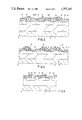
- FIG. 1 schematically shows a charge coupled image sensor device.
- FIG. 2 is a partly schematic, partly plan view of a part of the radiation-sensitive part of such an image sensor device.
- FIG. 3 is a cross-sectional view on the line III--III of the image sensor device of FIG. 2.
- FIG. 4 is a cross-sectional view on the line IV--IV of the image sensor device of FIG. 2.
- FIG. 5 is a cross-sectional view on the line V--V of the image sensor device of FIG. 2.
- FIG. 6 is a plan view of a part of the radiation-sensitive part of another image sensor device according to the invention.
- FIG. 7 is a cross-sectional view on the line VII--VII of the image sensor device of FIG. 6.
- FIG. 8 is a cross-sectional view on the line VIII--VIII of the image sensor device of FIG. 6.
- FIG. 1 shows a charge coupled image sensor device 1 of the so-called frame/field-transfer type.
- Such an image sensor device comprises a radiation-sensitive sensor part 2.
- a pattern of electric charge carriers corresponding to the radiation image is formed in part 2 during a given exposure period. After the exposure period, the pattern of electric charge carriers is stored temporarily in the storage part 3.
- the pattern is sequentially read from storage part 3 by the shift register 4.
- This charge pattern can be read by techniques known per se. If desired, the signals obtained may be amplified before further processing by the amplifier 22.
- the image sensor device (FIGS. 2-5) comprises a semiconductor body 5.
- Body 5 is composed, for example, an n-type silicon substrate 6 having a resistivity of approximately 10 ⁇ .cm (approximately 5.10 14 donor atoms/cm 3 ).
- a p-type region 7 is deposited on substrate 6. Region 7 has a dopant concentration of approximately 3.10 15 acceptor atoms/cm 3 .
- the p-type region 7 may be deposited, for example, by epitaxial growth.
- FIG. 1 At the major surface 8 of the semiconductor body 5, there are defined a plurality of mutually separated, substantially parallel charge transfer channels (in FIG. 1 designated by reference numeral 9). Charge transport in these channels is indicated schematically in FIG. 1 by arrows 10.
- the charge transfer device or ccd uses bulk transport, and is therefore known as a pccd or bccd.
- the charge transfer channels are n-type regions 11 which are mutually separated by p-type regions 12 (FIG. 4).
- the n-type regions in this example each have an average impurity concentration of approximately 10 16 atoms/cm 3 , a depth of approximately 1 ⁇ m, a width of approximately 3.5 ⁇ m.
- the p-type regions 12 each have a surface concentration of approximately 10 18 atoms/cm 3 , a surface width of approximately 5 ⁇ m, and a depth approximately 0.5 ⁇ m into the semiconductor body 5.
- the major surface 8 is coated with a layer 13 of insulating material, for example silicon oxide.
- a layer 13 of insulating material for example silicon oxide.
- a first set of electrodes for producing potential wells in the semiconductor material for charge storage and charge transport.
- the first set of electrodes 15 and 16 are mutually insulated and extend in a direction perpendicular to the direction of the charge transport channels. Electrodes 15 and 16 extend in equal intervals of approximately 4 ⁇ m along the channel.
- the electrodes are made of, for example, polycrystalline silicon. Since polycrystalline silicon is comparatively poorly transparent to short wavelength (blue) light, the electrode system is provided with windows 14. Through windows 14, light (especially blue light) can penetrate into the semiconductor body 5 and can produce charge carriers therein.
- the electrode system therefore comprises a second set of electrodes 17 and a third set of electrodes 18. Electrodes 17 and 18 are located mainly transverse to the transfer channels 11. However, projecting parts 19 and 20 of electrodes 17 and 19 extend above these channels 11 in a direction parallel to the charge transport direction.
- the electrodes 17 and 18 and the electrodes 15 and 16 bound the radiation-transparent windows 14 in directions transverse to the channels 11.
- the projecting parts 19 and 20 of the electrodes 17 and 18 bound the windows 14 in the directions of the channels 11.
- the projecting parts 20 of the electrode 18 overlap, in part, a next electrode 17 located on the other side of the electrode 18. Due to the fact that the charge transfer channels 11 are thus covered entirely by the electrode system, no loss of transport efficiency occurs when charge is transported under these electrodes.
- the electrodes 15, 16, 17 and 18 constitute an electrode system for a four phase clock system.
- charge carriers produced by radiation can now be alternately integrated in a similar manner in adjacent regions.
- the charge packets are alternately collected under the projecting parts 19 and 20 of the electrodes 17 and 18, respectively.
- charge carriers are produced. Blue light produces charge carriers substantially only down to a depth of approximately 0.1 ⁇ m, in particular in the p-type region 12, which is left exposed by the windows 14.
- the holes produced due to this radiation remain in the p-type region 12.
- the electrons produced migrate over to the adjacent charge transfer channels 11 due to the application of a voltage to the electrode 17 or to the electrode 18 such that potential wells for electrons are obtained in the charge transfer channels under the electrodes 17 and 18.
- a voltage is first applied to the electrodes 17 such that potential wells are formed under the projecting parts 19 in the channel regions 11.
- Charge packets are collected in the potential wells in the manner described above.
- the projecting parts 15 then each have, for example, a length of 5 ⁇ m, and a width of 3.6 ⁇ m, and a separation of 5 ⁇ m.
- the charge packets are transported to the storage part 3, by applying suitably chosen clock voltages to the electrodes 15, 16, 17, and 19, for further processing.
- charge is continuously collected under the electrode parts 19 and 20 of the electrodes 17 and 18. After the integration periods, during the first half of an image period for example, the charge packets collected under the electrode parts 19 are added to those collected under the electrode parts 20. During the second half, the charge packets collected under the electrode parts 20 are added to those collected under the parts 19. The adding process is effected so that the charge transport takes place in the direction of the arrows 10.
- the storage part 3 need not collect radiation and consequently need not be provided with windows. Therefore, as a whole it can be provided on a considerably smaller surface area than the radiation-sensitive part 2.
- the required charge transport clock signals can be obtained, like the clock signals for the shift register 4, in a well manner.
- the clock signals can be obtained by shift registers (not shown in FIG. 1).
- the device can be manufactured in a usual manner. After a p-type epitaxial layer 7 has been grown onto the n-type substrate 6, n-type channels 11 are formed in this layer 7 by implantation or diffusion. A thin oxide layer 13 is deposited on the surface 8.
- the electrodes 15 and 16 are formed in a well known manner, preferably from polycrystalline silicon on oxide layer 13. After an oxidation step for electrically insulating the electrodes 15 and 16, the electrodes 17 and 19 are formed from polycrystalline silicon. After these electrodes have been electrically insulated by another oxidation step, the electrodes 18 and 20 are formed. After the electrode system has been finished in this manner, the regions 12 are formed by an implantation step.
- the device shown in FIGS. 1 to 5 can be used in a simple manner with a two phase clock system. This can be done by applying a potential difference between the electrodes 16 and 18, and the electrodes 15 and 17 so that asymmetrical potential wells are obtained.
- the potential difference which is indicated schematically in FIG. 2 by the voltage sources 21, may be applied, for example, by a voltage divider. This is described in Dutch Patent Application No. 7,200,519 (corresponding to U.S. Pat. Nos. 3,758,794 and 3,760,202).
- the potential difference may alternatively be applied by a capacitive coupling, as described in Dutch Patent Application No. 7,114,859 (corresponding to U.S. Pat. No. 3,921,195).
- An additional advantage of this configuration is the low relative capacitance between the two clock phases because these phases overlap each other over a very small part.
- the electrodes 17 and 18 are constructed so that they fully define the windows 14. Although this is achieved at the expense of reducing the surface area, all the windows 14 are now fully identical. This can be manufactured by using the same mask in the manufacture of the relatively shifted electrodes 17 and 18. Due to the fact that the electrodes 15 and 16 now do not bound the the windows 14, tolerances between these electrodes and the electrodes 17 and 18 no longer influence the size of the windows.
- electrodes 17 and 18 may be constructed as long strips with openings without fully defining the windows, for example when the distance between the electrodes 15 and 16 is smaller than the dimensions of the openings in the transport device.
- other kinds of transport devices may be used, such as, for example, bucket brigade registers and surface ccd's.
Applications Claiming Priority (2)
| Application Number | Priority Date | Filing Date | Title |
|---|---|---|---|
| NL8300366A NL8300366A (nl) | 1983-02-01 | 1983-02-01 | Beeldopneeminrichting. |
| NL8300366 | 1983-02-01 |
Related Parent Applications (1)
| Application Number | Title | Priority Date | Filing Date |
|---|---|---|---|
| US06573441 Continuation | 1984-01-24 |
Publications (1)
| Publication Number | Publication Date |
|---|---|
| US4757365A true US4757365A (en) | 1988-07-12 |
Family
ID=19841329
Family Applications (1)
| Application Number | Title | Priority Date | Filing Date |
|---|---|---|---|
| US07/048,474 Expired - Fee Related US4757365A (en) | 1983-02-01 | 1987-05-06 | CCD image sensor with substantially identical integration regions |
Country Status (15)
| Country | Link |
|---|---|
| US (1) | US4757365A (sv) |
| JP (1) | JP2628622B2 (sv) |
| AT (1) | AT393181B (sv) |
| AU (1) | AU564837B2 (sv) |
| BE (1) | BE898789A (sv) |
| CA (1) | CA1214248A (sv) |
| DE (1) | DE3402017A1 (sv) |
| ES (1) | ES8500509A1 (sv) |
| FR (1) | FR2540291B1 (sv) |
| GB (1) | GB2134710B (sv) |
| HK (1) | HK6387A (sv) |
| IE (1) | IE55293B1 (sv) |
| IT (1) | IT1173508B (sv) |
| NL (1) | NL8300366A (sv) |
| SE (1) | SE460001B (sv) |
Cited By (4)
| Publication number | Priority date | Publication date | Assignee | Title |
|---|---|---|---|---|
| US5317174A (en) * | 1993-02-19 | 1994-05-31 | Texas Instruments Incorporated | Bulk charge modulated device photocell |
| US5338948A (en) * | 1991-05-10 | 1994-08-16 | Photometrics, Ltd. | Charge-coupled device with open gate structure |
| US5393971A (en) * | 1993-06-14 | 1995-02-28 | Ball Corporation | Radiation detector and charge transport device for use in signal processing systems having a stepped potential gradient means |
| US6242768B1 (en) * | 1998-06-24 | 2001-06-05 | Lg Semicon Co., Ltd. | Charge coupled device and a driving method thereof |
Families Citing this family (6)
| Publication number | Priority date | Publication date | Assignee | Title |
|---|---|---|---|---|
| NL8401311A (nl) * | 1984-04-24 | 1985-11-18 | Philips Nv | Ladingsgekoppelde halfgeleiderinrichting met dynamische besturing. |
| FR2636171B1 (fr) * | 1988-08-10 | 1990-11-09 | Philips Nv | Dispositif capteur d'images du type a transfert de trame |
| NL9000776A (nl) * | 1990-04-03 | 1991-11-01 | Philips Nv | Werkwijze ter vervaardiging van een ladingsgekoppelde beeldopneeminrichting, alsmede beeldopneeminrichting verkregen door deze werkwijze. |
| CA2045363A1 (en) * | 1990-10-01 | 1992-04-02 | Selim S. Bencuya | Ccd frame transfer device with simplified and improved well and electrode structure |
| EP0625800B1 (en) * | 1993-05-21 | 2001-09-26 | Koninklijke Philips Electronics N.V. | Charge coupled imaging device |
| US6238131B1 (en) | 1999-05-27 | 2001-05-29 | Deere & Company | Draper belt connector assembly for a harvesting machine |
Citations (5)
| Publication number | Priority date | Publication date | Assignee | Title |
|---|---|---|---|---|
| US3758794A (en) * | 1971-01-14 | 1973-09-11 | Rca Corp | Charge coupled shift registers |
| US3921195A (en) * | 1970-10-29 | 1975-11-18 | Bell Telephone Labor Inc | Two and four phase charge coupled devices |
| US4141024A (en) * | 1975-09-25 | 1979-02-20 | Sony Corporation | Solid state image sensing device |
| US4194213A (en) * | 1974-12-25 | 1980-03-18 | Sony Corporation | Semiconductor image sensor having CCD shift register |
| US4463367A (en) * | 1980-02-19 | 1984-07-31 | U.S. Philips Corporation | Frame-transfer charge-coupled image sensor device having channel sounding regions below light-admitting windows |
Family Cites Families (3)
| Publication number | Priority date | Publication date | Assignee | Title |
|---|---|---|---|---|
| CA1075811A (en) * | 1970-10-29 | 1980-04-15 | George E. Smith | Charge coupled device |
| JPS5685981A (en) * | 1979-12-15 | 1981-07-13 | Sharp Corp | Solid image pickup apparatus |
| JPS57958U (sv) * | 1980-05-29 | 1982-01-06 |
-
1983
- 1983-02-01 NL NL8300366A patent/NL8300366A/nl not_active Application Discontinuation
-
1984
- 1984-01-21 DE DE19843402017 patent/DE3402017A1/de not_active Ceased
- 1984-01-26 CA CA000446076A patent/CA1214248A/en not_active Expired
- 1984-01-27 GB GB08402262A patent/GB2134710B/en not_active Expired
- 1984-01-27 AU AU23848/84A patent/AU564837B2/en not_active Ceased
- 1984-01-27 SE SE8400404A patent/SE460001B/sv not_active IP Right Cessation
- 1984-01-27 IT IT19353/84A patent/IT1173508B/it active
- 1984-01-30 BE BE0/212303A patent/BE898789A/fr not_active IP Right Cessation
- 1984-01-30 JP JP59014974A patent/JP2628622B2/ja not_active Expired - Lifetime
- 1984-01-30 AT AT292/84A patent/AT393181B/de not_active IP Right Cessation
- 1984-01-30 ES ES529277A patent/ES8500509A1/es not_active Expired
- 1984-01-30 IE IE208/84A patent/IE55293B1/en unknown
- 1984-02-01 FR FR8401555A patent/FR2540291B1/fr not_active Expired
-
1987
- 1987-01-15 HK HK63/87A patent/HK6387A/xx not_active IP Right Cessation
- 1987-05-06 US US07/048,474 patent/US4757365A/en not_active Expired - Fee Related
Patent Citations (6)
| Publication number | Priority date | Publication date | Assignee | Title |
|---|---|---|---|---|
| US3921195A (en) * | 1970-10-29 | 1975-11-18 | Bell Telephone Labor Inc | Two and four phase charge coupled devices |
| US3758794A (en) * | 1971-01-14 | 1973-09-11 | Rca Corp | Charge coupled shift registers |
| US3760202A (en) * | 1971-01-14 | 1973-09-18 | Rca Corp | Input circuits for charged-coupled circuits |
| US4194213A (en) * | 1974-12-25 | 1980-03-18 | Sony Corporation | Semiconductor image sensor having CCD shift register |
| US4141024A (en) * | 1975-09-25 | 1979-02-20 | Sony Corporation | Solid state image sensing device |
| US4463367A (en) * | 1980-02-19 | 1984-07-31 | U.S. Philips Corporation | Frame-transfer charge-coupled image sensor device having channel sounding regions below light-admitting windows |
Non-Patent Citations (2)
| Title |
|---|
| Abe et al, "A CCD Imager with SiO2 Exposed Photosensor Array", IEEE Int. Electron Devices Meeting (12/77), pp. 542-545. |
| Abe et al, A CCD Imager with SiO 2 Exposed Photosensor Array , IEEE Int. Electron Devices Meeting (12/77), pp. 542 545. * |
Cited By (4)
| Publication number | Priority date | Publication date | Assignee | Title |
|---|---|---|---|---|
| US5338948A (en) * | 1991-05-10 | 1994-08-16 | Photometrics, Ltd. | Charge-coupled device with open gate structure |
| US5317174A (en) * | 1993-02-19 | 1994-05-31 | Texas Instruments Incorporated | Bulk charge modulated device photocell |
| US5393971A (en) * | 1993-06-14 | 1995-02-28 | Ball Corporation | Radiation detector and charge transport device for use in signal processing systems having a stepped potential gradient means |
| US6242768B1 (en) * | 1998-06-24 | 2001-06-05 | Lg Semicon Co., Ltd. | Charge coupled device and a driving method thereof |
Also Published As
| Publication number | Publication date |
|---|---|
| SE8400404D0 (sv) | 1984-01-27 |
| JPS59144170A (ja) | 1984-08-18 |
| IT1173508B (it) | 1987-06-24 |
| ES529277A0 (es) | 1984-10-01 |
| GB2134710A (en) | 1984-08-15 |
| IE840208L (en) | 1984-08-01 |
| IE55293B1 (en) | 1990-08-01 |
| DE3402017A1 (de) | 1984-08-02 |
| GB2134710B (en) | 1986-07-02 |
| HK6387A (en) | 1987-01-23 |
| AT393181B (de) | 1991-08-26 |
| FR2540291B1 (fr) | 1986-12-12 |
| ATA29284A (de) | 1991-01-15 |
| JP2628622B2 (ja) | 1997-07-09 |
| FR2540291A1 (fr) | 1984-08-03 |
| GB8402262D0 (en) | 1984-02-29 |
| CA1214248A (en) | 1986-11-18 |
| NL8300366A (nl) | 1984-09-03 |
| SE460001B (sv) | 1989-08-28 |
| AU564837B2 (en) | 1987-08-27 |
| SE8400404L (sv) | 1984-08-02 |
| AU2384884A (en) | 1984-08-02 |
| BE898789A (fr) | 1984-07-30 |
| IT8419353A0 (it) | 1984-01-27 |
| ES8500509A1 (es) | 1984-10-01 |
Similar Documents
| Publication | Publication Date | Title |
|---|---|---|
| US4074302A (en) | Bulk channel charge coupled semiconductor devices | |
| CA1128649A (en) | Imaging devices | |
| JP2686914B2 (ja) | 線形固体撮像素子 | |
| US4757365A (en) | CCD image sensor with substantially identical integration regions | |
| US3995302A (en) | Transfer gate-less photosensor configuration | |
| US4878102A (en) | Charge-coupled device | |
| CA1187612A (en) | Charge coupled device | |
| US5164807A (en) | Charge-coupled devices with locally widened electrodes | |
| US4242692A (en) | Charge transfer device which has a pair of straight portions joined by a direction changing portion | |
| JPS588150B2 (ja) | 電荷結合半導体装置の動作方法 | |
| US4639940A (en) | Charge coupled device with meander channel and elongated, straight, parallel gate electrodes | |
| JPS62126667A (ja) | 固体撮像素子 | |
| JP2699841B2 (ja) | 固体撮像装置 | |
| US4141024A (en) | Solid state image sensing device | |
| US4207477A (en) | Bulk channel CCD with switchable draining of minority charge carriers | |
| GB2097186A (en) | Charge-coupled device | |
| US4463367A (en) | Frame-transfer charge-coupled image sensor device having channel sounding regions below light-admitting windows | |
| US7446353B2 (en) | Solid-state imaging apparatus and charge transfer apparatus | |
| JPH0661469A (ja) | Ccd映像素子 | |
| US5223727A (en) | Charge-coupled device having an improved electrode structure | |
| US4479201A (en) | Serpentine charge coupled device | |
| US4862235A (en) | Electrode structure for a corner turn in a series-parallel-series charge coupled device | |
| US4726049A (en) | Charge-coupled device input with complementary signal-dependent charge packets | |
| GB2105111A (en) | Charge-transfer device memory with drain for parasitic charge carriers | |
| JPS5849066B2 (ja) | 電荷転送装置 |
Legal Events
| Date | Code | Title | Description |
|---|---|---|---|
| FPAY | Fee payment |
Year of fee payment: 4 |
|
| FEPP | Fee payment procedure |
Free format text: PAYOR NUMBER ASSIGNED (ORIGINAL EVENT CODE: ASPN); ENTITY STATUS OF PATENT OWNER: LARGE ENTITY |
|
| FPAY | Fee payment |
Year of fee payment: 8 |
|
| REMI | Maintenance fee reminder mailed | ||
| LAPS | Lapse for failure to pay maintenance fees | ||
| FP | Lapsed due to failure to pay maintenance fee |
Effective date: 20000712 |
|
| STCH | Information on status: patent discontinuation |
Free format text: PATENT EXPIRED DUE TO NONPAYMENT OF MAINTENANCE FEES UNDER 37 CFR 1.362 |