US5338948A - Charge-coupled device with open gate structure - Google Patents
Charge-coupled device with open gate structure Download PDFInfo
- Publication number
- US5338948A US5338948A US08/033,190 US3319093A US5338948A US 5338948 A US5338948 A US 5338948A US 3319093 A US3319093 A US 3319093A US 5338948 A US5338948 A US 5338948A
- Authority
- US
- United States
- Prior art keywords
- charge
- coupled device
- set forth
- vertical elements
- substrate
- Prior art date
- Legal status (The legal status is an assumption and is not a legal conclusion. Google has not performed a legal analysis and makes no representation as to the accuracy of the status listed.)
- Expired - Lifetime
Links
- 239000004065 semiconductor Substances 0.000 claims abstract description 14
- 239000000758 substrate Substances 0.000 claims abstract description 8
- 239000007943 implant Substances 0.000 claims description 9
- 239000004020 conductor Substances 0.000 claims description 8
- VYPSYNLAJGMNEJ-UHFFFAOYSA-N Silicium dioxide Chemical compound O=[Si]=O VYPSYNLAJGMNEJ-UHFFFAOYSA-N 0.000 claims description 4
- 239000000463 material Substances 0.000 claims description 4
- ZOXJGFHDIHLPTG-UHFFFAOYSA-N Boron Chemical compound [B] ZOXJGFHDIHLPTG-UHFFFAOYSA-N 0.000 claims description 3
- 229910052796 boron Inorganic materials 0.000 claims description 3
- BHEPBYXIRTUNPN-UHFFFAOYSA-N hydridophosphorus(.) (triplet) Chemical compound [PH] BHEPBYXIRTUNPN-UHFFFAOYSA-N 0.000 claims description 3
- 229910021420 polycrystalline silicon Inorganic materials 0.000 claims description 3
- 229920005591 polysilicon Polymers 0.000 claims description 2
- 235000012239 silicon dioxide Nutrition 0.000 claims description 2
- 239000000377 silicon dioxide Substances 0.000 claims description 2
- 239000011248 coating agent Substances 0.000 claims 1
- 238000000576 coating method Methods 0.000 claims 1
- 239000011810 insulating material Substances 0.000 claims 1
- 238000001208 nuclear magnetic resonance pulse sequence Methods 0.000 claims 1
- 239000010410 layer Substances 0.000 description 3
- 206010034960 Photophobia Diseases 0.000 description 2
- 208000013469 light sensitivity Diseases 0.000 description 2
- 239000002344 surface layer Substances 0.000 description 2
- 238000003491 array Methods 0.000 description 1
- 238000000034 method Methods 0.000 description 1
Images


Classifications
-
- H—ELECTRICITY
- H01—ELECTRIC ELEMENTS
- H01L—SEMICONDUCTOR DEVICES NOT COVERED BY CLASS H10
- H01L29/00—Semiconductor devices specially adapted for rectifying, amplifying, oscillating or switching and having potential barriers; Capacitors or resistors having potential barriers, e.g. a PN-junction depletion layer or carrier concentration layer; Details of semiconductor bodies or of electrodes thereof ; Multistep manufacturing processes therefor
- H01L29/40—Electrodes ; Multistep manufacturing processes therefor
- H01L29/43—Electrodes ; Multistep manufacturing processes therefor characterised by the materials of which they are formed
- H01L29/435—Resistive materials for field effect devices, e.g. resistive gate for MOSFET or MESFET
-
- H—ELECTRICITY
- H01—ELECTRIC ELEMENTS
- H01L—SEMICONDUCTOR DEVICES NOT COVERED BY CLASS H10
- H01L27/00—Devices consisting of a plurality of semiconductor or other solid-state components formed in or on a common substrate
- H01L27/14—Devices consisting of a plurality of semiconductor or other solid-state components formed in or on a common substrate including semiconductor components sensitive to infrared radiation, light, electromagnetic radiation of shorter wavelength or corpuscular radiation and specially adapted either for the conversion of the energy of such radiation into electrical energy or for the control of electrical energy by such radiation
- H01L27/144—Devices controlled by radiation
- H01L27/146—Imager structures
- H01L27/148—Charge coupled imagers
- H01L27/14831—Area CCD imagers
Definitions
- This invention relates to Charge-Coupled Devices (CCDs) and more particularly to CCDs with improved light capturing capabilities.
- Charge-coupled devices are in wide spread commercial use. Such devices are available in linear arrays and in two dimensional array form.
- the cells, or light sensing elements, of a 2-dimensional CCD array are arranged in rows or columns and operated in the fashion of a parallel set of shift registers to move along the rows electrical charges, representative of a spatial distribution of incident light intensities, to a (column) shift register for read out.
- the charges are moved along the rows and columns, while the CCD is shuttered from light between exposures, by a multi-phase electrical gate structure, as is well understood in the art.
- the gate structure is formed on the surface of the semiconductor wafer in which the light-sensitive array of cells of the CCD are defined.
- the structure is defined by thin layers of polycrystalline silicon deposited, via photolithographic techniques, in a multi-layer, partially overlapping configuration which partially obstructs the passage of light to the semiconductor surface.
- the light-sensing characteristics of a CCD array is reduced by the conductor structure required to move the representative charges generated in the CCD by incident light.
- the present invention is based on the realization that the multi-phase, electrically-conducting gate structure of a CCD can be configured to expose relatively large areas of the surface of the semiconductor substrate and that the light gathering capability of a CCD with an open gate structure would be substantially improved over that of prior art CCDs.
- FIG. 1 is a schematic side view of a prior art CCD structure illustrating the potential wells generated therein during a three phase operation;
- FIG. 2 is an enlarged top view of a representative segment of a prior art CCD showing an overlapping, multi-phase gate electrode configuration with conventional channel stops;
- FIG. 3 is an enlarged top view of a representative segment of a CCD with an open gate electrode structure in accordance with the principles of this invention.
- FIGS. 1 and 2 show schematic side and top views of a prior art CCD segment 10.
- the CCD includes a three-phase polysilicon gate structure comprising electrodes 11, 12, and 13; 14, 15, and 16; and 17, 18, and 19 (shown only in FIG. 2).
- the view of figure two is taken orthogonally to that of FIG. 1.
- Segment 10 typically comprises a semiconductor wafer of P-conductivity type with an N-type buried implant and with an insulating surface layer of silicon dioxide as is well known. Only the N-type surface layer and oxide layers are shown in FIG. 1.
- CCD array The purpose of a CCD array is to store information quanta temporarily, each quanta represented by the presence or absence of a packet of charge, and to transfer the quanta from the left in FIG. 1 to an output to the right.
- the movement of quanta is carried out by adjusting the voltages on the electrodes or gates which are driven in a three phase manner in the illustrative embodiment. Specifically, the gates, as viewed in FIG. 2, are driven to provide a potential well for charge quanta beneath every third electrode. By driving the electrodes in a three phase manner, the potential wells are moved to the right, as viewed in FIG. 1.
- the charge quanta are confined within the wells and, accordingly, move with the wells as is well understood.
- the quanta also are confined to three columns in the representative segment by familiar channel stops 21, 22, and 23 shown in FIG. 2.
- Potential wells are formed by applying patterns of positive voltages to electrodes 11 and 13 (for N-type implants) and a higher positive voltage to electrode 12. Since electrodes 11, 14, and 17; 12, 15, and 18; and 13, 16, and 19 are connected in sets, a potential well is formed simultaneously beneath electrodes 11, 14, and 17 during a third phase of operation; beneath electrodes 12, 15, and 18 during a first phase of operation and beneath electrodes 13, 16, and 19 during a second phase of operation thus moving a pattern of wells from left to right as viewed in FIG. 1. The positions of the wells during the three phases of operation are represented by the dashed lines so designated in FIG. 1.
- the prior art gate structure of FIG. 1 comprises overlapping electrical conductors which are deposited in a multi-layered configuration and which covers the entire semiconductor surface.
- the amount of light actually incident to the semiconductor surface is reduced.
- Efforts have been made to increase the light sensitivity of CCDs by the choice of materials for the electrode structure and by the reduction of the thickness of the electrodes.
- incident light is reduced by a factor of 40 to 100 percent, depending upon the wavelength of the incident light, over that which would impinge the semiconductor in the absence of the gate electrodes.
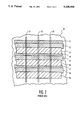
- FIG. 3 shows a segment 30 of a CCD with an open gate structure in accordance with the principles of this invention.
- the gate structure includes electrical conductors 31, 32, and 33; 34, 35, and 36; and 37, 38, and 39 arranged from left to right as viewed in the figure.
- the electrodes are driven in a three phase manner as is the prior art device of FIG. 1.
- each individual electrode has a series of shallow H-shaped geometries extending along a horizontal axis, as viewed.
- the vertically-oriented elements only of the H-shaped geometries overlap one another thus leaving exposed semiconductor surface area 40 unobstructed to incident light.
- Channel stops 50, 51, and 52 confine any charge moved from top to bottom in the figure to the respective columns for parallel shift register operation in conventional fashion.
- the overlap between the vertical elements of the H-shaped geometries is indicated by the lines 54 and 55 in FIG. 3. Such overlap permits the requisite three phase operation.
- a Phosphorous (N) implant is normally made over the entire CCD surface.
- Phosphorous (N) implant is normally made over the entire CCD surface.
- a shallow Boron (P) implant may be added under the first or second phase gate for "MPP" or "inverted” operation to lower dark current.
- the channel stops 50, 51, and 52 of FIG. 3, in practice, are made relatively wide to overlap the parallel gates.
- the extent of the channel stops is indicated by the broken lines at 56 in FIG. 3.
- the overlap of the channel stops enables the surface potential of the "open" areas to be controlled.
Landscapes
- Engineering & Computer Science (AREA)
- Power Engineering (AREA)
- Physics & Mathematics (AREA)
- Microelectronics & Electronic Packaging (AREA)
- Condensed Matter Physics & Semiconductors (AREA)
- General Physics & Mathematics (AREA)
- Computer Hardware Design (AREA)
- Ceramic Engineering (AREA)
- Electromagnetism (AREA)
- Solid State Image Pick-Up Elements (AREA)
Abstract
Description
Claims (10)
Priority Applications (1)
| Application Number | Priority Date | Filing Date | Title |
|---|---|---|---|
| US08/033,190 US5338948A (en) | 1991-05-10 | 1993-03-16 | Charge-coupled device with open gate structure |
Applications Claiming Priority (2)
| Application Number | Priority Date | Filing Date | Title |
|---|---|---|---|
| US69845391A | 1991-05-10 | 1991-05-10 | |
| US08/033,190 US5338948A (en) | 1991-05-10 | 1993-03-16 | Charge-coupled device with open gate structure |
Related Parent Applications (1)
| Application Number | Title | Priority Date | Filing Date |
|---|---|---|---|
| US69845391A Continuation-In-Part | 1991-05-10 | 1991-05-10 |
Publications (1)
| Publication Number | Publication Date |
|---|---|
| US5338948A true US5338948A (en) | 1994-08-16 |
Family
ID=24805318
Family Applications (1)
| Application Number | Title | Priority Date | Filing Date |
|---|---|---|---|
| US08/033,190 Expired - Lifetime US5338948A (en) | 1991-05-10 | 1993-03-16 | Charge-coupled device with open gate structure |
Country Status (1)
| Country | Link |
|---|---|
| US (1) | US5338948A (en) |
Cited By (6)
| Publication number | Priority date | Publication date | Assignee | Title |
|---|---|---|---|---|
| US5644121A (en) * | 1994-12-07 | 1997-07-01 | Nec Corporation | Solid state image sensor |
| US5818035A (en) * | 1995-09-11 | 1998-10-06 | Gatan, Inc. | Optically coupled large-format solid state imaging apparatus having edges of an imaging device |
| US5965910A (en) * | 1997-04-29 | 1999-10-12 | Ohmeda Inc. | Large cell charge coupled device for spectroscopy |
| US6107655A (en) * | 1997-08-15 | 2000-08-22 | Eastman Kodak Company | Active pixel image sensor with shared amplifier read-out |
| US6448592B1 (en) * | 1996-09-10 | 2002-09-10 | Koninklijke Philips Electronics N.V. | Charge coupled device, and method of manufacturing such a device |
| CN110610955A (en) * | 2019-09-09 | 2019-12-24 | 中国电子科技集团公司第四十四研究所 | CCD grid structure for reducing overlapping coupling |
Citations (10)
| Publication number | Priority date | Publication date | Assignee | Title |
|---|---|---|---|---|
| US3961355A (en) * | 1972-06-30 | 1976-06-01 | International Business Machines Corporation | Semiconductor device having electrically insulating barriers for surface leakage sensitive devices and method of forming |
| JPS5898961A (en) * | 1981-12-09 | 1983-06-13 | Toshiba Corp | Charge transfer device |
| JPS59113661A (en) * | 1982-12-20 | 1984-06-30 | Sanyo Electric Co Ltd | Solid state image pickup element |
| JPS59159564A (en) * | 1983-03-02 | 1984-09-10 | Sony Corp | Solid-state photo-electric conversion device |
| US4663771A (en) * | 1981-08-29 | 1987-05-05 | Sony Corporation | Solid state image pickup device in which the transfer gate areas are supplied with negative voltage during the vertical transfer period and light receiving period but not when the positive readout pulse period is applied |
| JPS62293762A (en) * | 1986-06-13 | 1987-12-21 | Matsushita Electric Ind Co Ltd | Solid-state image pickup device |
| US4757365A (en) * | 1983-02-01 | 1988-07-12 | U.S. Philips Corporation | CCD image sensor with substantially identical integration regions |
| US4805026A (en) * | 1986-02-18 | 1989-02-14 | Nec Corporation | Method for driving a CCD area image sensor in a non-interlace scanning and a structure of the CCD area image sensor for driving in the same method |
| US4970567A (en) * | 1987-11-23 | 1990-11-13 | Santa Barbara Research Center | Method and apparatus for detecting infrared radiation |
| US5043819A (en) * | 1989-12-05 | 1991-08-27 | Samsung Electronics Co., Ltd. | CCD solid state image sensor with two horizontal transfer CCDs corresponding to both odd and even columns of elements |
-
1993
- 1993-03-16 US US08/033,190 patent/US5338948A/en not_active Expired - Lifetime
Patent Citations (10)
| Publication number | Priority date | Publication date | Assignee | Title |
|---|---|---|---|---|
| US3961355A (en) * | 1972-06-30 | 1976-06-01 | International Business Machines Corporation | Semiconductor device having electrically insulating barriers for surface leakage sensitive devices and method of forming |
| US4663771A (en) * | 1981-08-29 | 1987-05-05 | Sony Corporation | Solid state image pickup device in which the transfer gate areas are supplied with negative voltage during the vertical transfer period and light receiving period but not when the positive readout pulse period is applied |
| JPS5898961A (en) * | 1981-12-09 | 1983-06-13 | Toshiba Corp | Charge transfer device |
| JPS59113661A (en) * | 1982-12-20 | 1984-06-30 | Sanyo Electric Co Ltd | Solid state image pickup element |
| US4757365A (en) * | 1983-02-01 | 1988-07-12 | U.S. Philips Corporation | CCD image sensor with substantially identical integration regions |
| JPS59159564A (en) * | 1983-03-02 | 1984-09-10 | Sony Corp | Solid-state photo-electric conversion device |
| US4805026A (en) * | 1986-02-18 | 1989-02-14 | Nec Corporation | Method for driving a CCD area image sensor in a non-interlace scanning and a structure of the CCD area image sensor for driving in the same method |
| JPS62293762A (en) * | 1986-06-13 | 1987-12-21 | Matsushita Electric Ind Co Ltd | Solid-state image pickup device |
| US4970567A (en) * | 1987-11-23 | 1990-11-13 | Santa Barbara Research Center | Method and apparatus for detecting infrared radiation |
| US5043819A (en) * | 1989-12-05 | 1991-08-27 | Samsung Electronics Co., Ltd. | CCD solid state image sensor with two horizontal transfer CCDs corresponding to both odd and even columns of elements |
Cited By (7)
| Publication number | Priority date | Publication date | Assignee | Title |
|---|---|---|---|---|
| US5644121A (en) * | 1994-12-07 | 1997-07-01 | Nec Corporation | Solid state image sensor |
| US5818035A (en) * | 1995-09-11 | 1998-10-06 | Gatan, Inc. | Optically coupled large-format solid state imaging apparatus having edges of an imaging device |
| US6448592B1 (en) * | 1996-09-10 | 2002-09-10 | Koninklijke Philips Electronics N.V. | Charge coupled device, and method of manufacturing such a device |
| US5965910A (en) * | 1997-04-29 | 1999-10-12 | Ohmeda Inc. | Large cell charge coupled device for spectroscopy |
| US6107655A (en) * | 1997-08-15 | 2000-08-22 | Eastman Kodak Company | Active pixel image sensor with shared amplifier read-out |
| US6352869B1 (en) | 1997-08-15 | 2002-03-05 | Eastman Kodak Company | Active pixel image sensor with shared amplifier read-out |
| CN110610955A (en) * | 2019-09-09 | 2019-12-24 | 中国电子科技集团公司第四十四研究所 | CCD grid structure for reducing overlapping coupling |
Similar Documents
| Publication | Publication Date | Title |
|---|---|---|
| US4724470A (en) | Image sensor device having separate photosensor and charge storage | |
| US5210433A (en) | Solid-state CCD imaging device with transfer gap voltage controller | |
| CA1096969A (en) | Charge transfer device | |
| EP1091412B1 (en) | Charge transfer path having lengthwisely varying channel width and image pickup device using it | |
| US5040038A (en) | Solid-state image sensor | |
| US5338948A (en) | Charge-coupled device with open gate structure | |
| US6194242B1 (en) | Fabrication of solid-state imaging device having no transfer error of the signal charge from vertical horizontal charge-transfer section | |
| US4064524A (en) | Two-phase charge transfer device image sensor | |
| US4720746A (en) | Frame transfer CCD area image sensor with improved horizontal resolution | |
| US5902995A (en) | CCD image sensor with overflow barrier for discharging excess electrons at high speed | |
| US4085456A (en) | Charge transfer imaging devices | |
| US5196692A (en) | Photoelectric transducer switchable to a high-resolution or high-sensitivity mode | |
| US4433343A (en) | Extrinsic infrared detector with dopant site charge-neutralization | |
| US5345099A (en) | Semiconductor device | |
| GB2134710A (en) | Image sensor device | |
| KR930007532B1 (en) | Ccd imager of three dimension using soi structure and method for fabricating thereof | |
| US4141024A (en) | Solid state image sensing device | |
| US5290722A (en) | Method of making floating gate junction field effect transistor image sensor elements | |
| EP0132870B1 (en) | Radiation-sensitive semiconductor device | |
| US4721989A (en) | CCD with transfer channel at lower potential than supply channel | |
| US5741728A (en) | Method for manufacturing charge-coupled device with polygates having the same resistances | |
| US6218686B1 (en) | Charge coupled devices | |
| KR940004273B1 (en) | Different type vertical ccd structure | |
| US5986295A (en) | Charge coupled device | |
| KR100263467B1 (en) | Solid state image sensor and method of fabricating the same |
Legal Events
| Date | Code | Title | Description |
|---|---|---|---|
| AS | Assignment |
Owner name: PHOTOMETRICS LTD., ARIZONA Free format text: ASSIGNMENT OF ASSIGNORS INTEREST.;ASSIGNOR:SIMS, GARY R.;REEL/FRAME:006480/0933 Effective date: 19930304 |
|
| STPP | Information on status: patent application and granting procedure in general |
Free format text: APPLICATION UNDERGOING PREEXAM PROCESSING |
|
| FPAY | Fee payment |
Year of fee payment: 4 |
|
| AS | Assignment |
Owner name: ROPER HOLDINGS, INC., DELAWARE Free format text: ASSIGNMENT OF ASSIGNORS INTEREST;ASSIGNOR:ROPER SCIENTIFIC, INC.;REEL/FRAME:010024/0211 Effective date: 19990609 Owner name: ROPER SCIENTIFIC, INC., ARKANSAS Free format text: MERGER;ASSIGNORS:PHOTOMETRICS, LTD.;PRINCETON INSTRUMENTS, INC.;REEL/FRAME:010024/0217 Effective date: 19980513 |
|
| FEPP | Fee payment procedure |
Free format text: PAT HOLDER NO LONGER CLAIMS SMALL ENTITY STATUS, ENTITY STATUS SET TO UNDISCOUNTED (ORIGINAL EVENT CODE: STOL); ENTITY STATUS OF PATENT OWNER: LARGE ENTITY |
|
| REFU | Refund |
Free format text: REFUND - PAYMENT OF MAINTENANCE FEE, 8TH YR, SMALL ENTITY (ORIGINAL EVENT CODE: R284); ENTITY STATUS OF PATENT OWNER: LARGE ENTITY |
|
| REMI | Maintenance fee reminder mailed | ||
| FPAY | Fee payment |
Year of fee payment: 8 |
|
| SULP | Surcharge for late payment |
Year of fee payment: 7 |
|
| AS | Assignment |
Owner name: ROPINTASSCO HOLDINGS, L.P., GEORGIA Free format text: ASSIGNMENT OF ASSIGNORS INTEREST;ASSIGNOR:ROPER HOLDINGS, INC.;REEL/FRAME:014805/0957 Effective date: 20031128 |
|
| AS | Assignment |
Owner name: JPMORGAN CHASE BANK, TEXAS Free format text: SECURITY AGREEMENT;ASSIGNOR:ROPINTASSCO HOLDINGS, L.P.;REEL/FRAME:014981/0256 Effective date: 20040206 |
|
| FPAY | Fee payment |
Year of fee payment: 12 |
|
| AS | Assignment |
Owner name: ROPER HOLDINGS, INC., DELAWARE Free format text: ASSIGNMENT OF ASSIGNORS INTEREST;ASSIGNOR:ROPINTASSCO HOLDINGS, L.P.;REEL/FRAME:017314/0868 Effective date: 20060306 |
|
| AS | Assignment |
Owner name: ROPINTASSCO HOLDINGS, L.P., FLORIDA Free format text: TERMINATION AND RELEASE OF SECURITY;ASSIGNOR:JPMORGAN CHASE BANK, N.A.;REEL/FRAME:021281/0956 Effective date: 20080701 |
|
| AS | Assignment |
Owner name: ROPER SCIENTIFIC, INC., ARIZONA Free format text: ASSIGNMENT OF ASSIGNORS INTEREST;ASSIGNOR:ROPER HOLDINGS, INC.;REEL/FRAME:023660/0040 Effective date: 20091203 |