US5902995A - CCD image sensor with overflow barrier for discharging excess electrons at high speed - Google Patents
CCD image sensor with overflow barrier for discharging excess electrons at high speed Download PDFInfo
- Publication number
- US5902995A US5902995A US08/901,458 US90145897A US5902995A US 5902995 A US5902995 A US 5902995A US 90145897 A US90145897 A US 90145897A US 5902995 A US5902995 A US 5902995A
- Authority
- US
- United States
- Prior art keywords
- channels
- register
- electrodes
- horizontal
- charge packets
- Prior art date
- Legal status (The legal status is an assumption and is not a legal conclusion. Google has not performed a legal analysis and makes no representation as to the accuracy of the status listed.)
- Expired - Lifetime
Links
- 230000004888 barrier function Effects 0.000 title claims abstract description 63
- 238000007599 discharging Methods 0.000 title claims abstract description 12
- 239000004065 semiconductor Substances 0.000 claims description 26
- 239000000758 substrate Substances 0.000 claims description 11
- 239000012535 impurity Substances 0.000 claims description 6
- 238000000034 method Methods 0.000 claims description 6
- 108091006146 Channels Proteins 0.000 description 57
- VYPSYNLAJGMNEJ-UHFFFAOYSA-N Silicium dioxide Chemical compound O=[Si]=O VYPSYNLAJGMNEJ-UHFFFAOYSA-N 0.000 description 10
- 239000010408 film Substances 0.000 description 10
- 239000010410 layer Substances 0.000 description 10
- -1 boron ions Chemical class 0.000 description 9
- 229910052796 boron Inorganic materials 0.000 description 7
- 230000000694 effects Effects 0.000 description 5
- 230000008569 process Effects 0.000 description 5
- 229960001866 silicon dioxide Drugs 0.000 description 5
- 235000012239 silicon dioxide Nutrition 0.000 description 5
- 239000000377 silicon dioxide Substances 0.000 description 5
- 229910052698 phosphorus Inorganic materials 0.000 description 4
- 239000011574 phosphorus Substances 0.000 description 4
- 229920002120 photoresistant polymer Polymers 0.000 description 4
- 229910021420 polycrystalline silicon Inorganic materials 0.000 description 3
- 229920005591 polysilicon Polymers 0.000 description 3
- ZOXJGFHDIHLPTG-UHFFFAOYSA-N Boron Chemical compound [B] ZOXJGFHDIHLPTG-UHFFFAOYSA-N 0.000 description 2
- 102000004129 N-Type Calcium Channels Human genes 0.000 description 2
- 108090000699 N-Type Calcium Channels Proteins 0.000 description 2
- 230000005574 cross-species transmission Effects 0.000 description 2
- 238000010586 diagram Methods 0.000 description 2
- 239000002356 single layer Substances 0.000 description 2
- XUIMIQQOPSSXEZ-UHFFFAOYSA-N Silicon Chemical compound [Si] XUIMIQQOPSSXEZ-UHFFFAOYSA-N 0.000 description 1
- 230000002411 adverse Effects 0.000 description 1
- 230000008901 benefit Effects 0.000 description 1
- 230000015572 biosynthetic process Effects 0.000 description 1
- 230000008859 change Effects 0.000 description 1
- 238000005094 computer simulation Methods 0.000 description 1
- 230000005684 electric field Effects 0.000 description 1
- 238000003384 imaging method Methods 0.000 description 1
- 238000009413 insulation Methods 0.000 description 1
- 239000012212 insulator Substances 0.000 description 1
- 150000002500 ions Chemical class 0.000 description 1
- 238000004519 manufacturing process Methods 0.000 description 1
- 239000011159 matrix material Substances 0.000 description 1
- 230000003647 oxidation Effects 0.000 description 1
- 238000007254 oxidation reaction Methods 0.000 description 1
- 238000005036 potential barrier Methods 0.000 description 1
- 230000004044 response Effects 0.000 description 1
- 229910052710 silicon Inorganic materials 0.000 description 1
- 239000010703 silicon Substances 0.000 description 1
- 239000010409 thin film Substances 0.000 description 1
Images
Classifications
-
- H—ELECTRICITY
- H01—ELECTRIC ELEMENTS
- H01L—SEMICONDUCTOR DEVICES NOT COVERED BY CLASS H10
- H01L27/00—Devices consisting of a plurality of semiconductor or other solid-state components formed in or on a common substrate
- H01L27/14—Devices consisting of a plurality of semiconductor or other solid-state components formed in or on a common substrate including semiconductor components sensitive to infrared radiation, light, electromagnetic radiation of shorter wavelength or corpuscular radiation and specially adapted either for the conversion of the energy of such radiation into electrical energy or for the control of electrical energy by such radiation
- H01L27/144—Devices controlled by radiation
- H01L27/146—Imager structures
- H01L27/148—Charge coupled imagers
- H01L27/14887—Blooming suppression
Definitions
- the present invention relates generally to two-dimensional CCD (charge-coupled device) imaging device, and more specifically to such a CCD device capable of efficiently discharging undesired charge packets.
- the present invention is particularly suitable for CCD image sensors where large amounts of non-usable charge packets must be quickly discharged.
- Japanese Laid-Open Patent Specification Sho 62-154881 discloses a two-dimensional charge transfer device comprising a plurality of vertical registers for receiving electrons, or "charge packets" from a two-dimensional array of photodiodes and shifting them down to a horizontal register.
- the horizontal register includes overflow barrier regions and an overflow drain region. When excessive charge packets are produced, they overflow the barrier regions and are discharged through the drain region to the outside, while useful charge packets are diverted to a utilization circuit.
- the overflow barrier regions of this prior art device are formed into the shape of narrow channels to take advantage of what is known as the narrow channel effect of a semiconductor junction on a threshold voltage, i.e., when the channel width is reduced, the threshold voltage of the junction increases. Due to the narrow channel effect, the overflow channel regions are at such a potential that only surplus electrons are discharged to the outside.
- Japanese Laid-Open Patent Specification Sho 63-254767 discloses a single-layer diffused overflow barrier region extending between the overflow drain region and the edges of horizontal-register channels remote from the vertical registers.
- the disadvantage of the prior art is that the forming of this barrier region requires an additional photoresist process.
- the present invention provides a charge transfer device comprising an array of photodiodes, a plurality of vertical registers having a plurality of channels for receiving charge packets from the photodiodes and a plurality of electrodes for shifting the charge packets along the channels, and a horizontal register having a plurality of channels for receiving the charge packets from the vertical registers and a plurality of electrodes for successively shifting the charge packets across the channels.
- An overflow barrier region is provided that extends across and is embedded below the channels of the horizontal register for establishing a barrier potential.
- An overflow drain region is connected to the channels of the horizontal register for discharging charge packets which exceed the barrier potential.
- the present invention provides a charge transfer device comprising a first semiconductor region of first conductivity type on a substrate, an array of photodiodes on the first semiconductor region, a plurality of isolating channel regions of the first conductivity type embedded in the first semiconductor region for receiving charge packets from the photodiodes, a plurality of vertical-register channels of second conductivity type respectively on the channel regions, and a plurality of mutually overlapping vertical electrodes for shifting the charge packets along the vertical-register channels.
- a second semiconductor region of the first conductivity type is formed on the substrate, and an overflow barrier region of the first conductivity type is embedded in the second semiconductor region to a depth equal to the channel regions for establishing a barrier potential.
- a plurality of horizontal-register channels of second conductivity type are provided on the second semiconductor region respectively corresponding to the vertical-register channels to receive the charge packets therefrom, the horizontal-register channels overlying the overflow barrier region.
- a plurality of mutually overlapping horizontal electrodes are provided for shifting the charge packets across the horizontal-register channels.
- An overflow drain region of the second conductivity type is connected to the channels of the horizontal register for discharging charge packets which exceed the barrier potential established by the overflow barrier region.
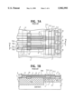
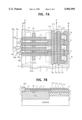
- FIG. 1A is a partial plan view of a prior art CCD image sensor
- FIG. 1B is a cross-sectional view of the prior art CCD image sensor taken along the lines 1B of FIG. 1A;
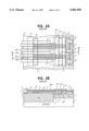
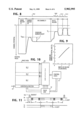
- FIG. 2A is a partial plan view of another prior art CCD image sensor
- FIG. 2B is a cross-sectional view of the prior art CCD image sensor taken along the lines 2B of FIG. 2A;
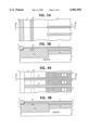
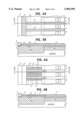
- FIGS. 3A, 4A, 5A, 6A and 7A are partial plan views showing successive stages of fabricating a CCD image sensor of the present invention
- FIGS. 3B, 4B, 5B, 6B and 7B are cross-sectional views taken along the lines 3B, 4B, 5B, 6B and 7B of FIGS. 3A, 4A, 5A, 6A and 7A, respectively;
- FIG. 8 is an illustration of a potential profile of the CCD image sensor of this invention taken along the line 8 of FIG. 7A;
- FIG. 9 is a graphic representation of the relationship between the overflow barrier potential as a function of the width of the overflow barrier region of this invention.
- FIG. 10 is a block diagram of the CCD image sensor and the circuitry for operating the sensor in an automatic focusing mode.
- FIG. 11 is a timing diagram of the vertical and horizontal shift pulses supplied to the CCD image sensor during the automatic focusing mode.
- a portion of the image area of the prior art CCD image sensor is generally represented as IA in which a two-dimensional array of photodiodes 8 are formed on a P - -type well 3 which is in turn formed on a substrate 1.
- a plurality of N-type semiconductor regions, or vertical-register channels 11, which are isolated from each other by channel stoppers 10, are formed on respective P-type insulating layers 4.
- the insulating layers 4 serve as isolators between the vertical-register channels 11 and the underlying P - -type well 3.
- a plurality of parallel, mutually overlapping vertical electrodes 13 extend across the vertical-register channels 11, forming a plurality of vertical resisters. Those vertical electrodes other than the final two electrodes are provided with openings for allowing light rays to impinge on the photodiodes 8.
- the horizontal register HR Adjacent to the final two vertical electrodes is the horizontal register HR which is formed by a plurality of N-type regions 9 arranged in parallel in a direction normal to the vertical channels 11. These N-type regions 9 are formed on a P-type well 2 as extensions of vertical-register channels 11 to receive charge packets therefrom and to move them along a path on the horizontal register.
- a plurality of P + -type overflow barrier regions 18 are diffused simultaneously with the P + -type channel stoppers 10 on the P-type well 2 adjacent the edges of N-type horizontal-register channels 9 remote from the image area.
- An N + -type diffused overflow drain region 12 is formed alongside the P + -type overflow barrier regions 18.
- a plurality of N - -type diffused thin isolating layers 15 are formed in parallel partially overlying the horizontal-register channels 9.
- a P + -type channel stopper 5 is formed alongside the overflow drain region 12.
- the device is coated with an insulator film 7 on which the vertical electrodes 13 of the vertical registers are provided, and a plurality of mutually overlapping electrodes 14 of the horizontal register HR are formed.
- Overflow barrier regions 18 are mutually spaced a distance D which is narrower than the length L of the underlying storage electrodes 14s1, 14s2 as measured along the length of the horizontal register. This produces what is known as the narrow channel effect on the threshold voltage of a semiconductor device. As a result, the overflow barrier regions 19 produce a potential barrier to a certain amount of charge packets. Therefore, when a large amount of unuseful electrons must be discharged from the device, they exceed the barrier potential and spill over the overflow barrier regions 19 and are discharged through the drain region 12.
- barrier regions 19 Unfortunately, the disadvantage of this narrow spacing of barrier regions 19 is that they produce a throttling effect on charge packets as they are discharged through the overflow drain 12, resulting in a low discharging speed.
- FIGS. 2A and 2B illustrate a practical implementation of a CCD image sensor according to the teaching is Specification.
- a P + -type diffused layer 19 is formed as an overflow barrier between the overflow drain region 12 and the ends of horizontal channels 9 remote from the vertical registers.
- the disadvantage of the prior art is that the forming of this diffused region requires an additional photoresist process.
- the device comprises an N-type silicon substrate 1 impurity-doped with a concentration of 2 ⁇ 10 14 cm -3 .
- a P-type well 2 with a concentration of 3 ⁇ 10 15 cm -3 with a thickness of 6 microns is formed below the surface of substrate 1 outside of the image area by injecting boron and then the injected boron is diffused under pressure.
- a P - -type well 3 is formed within the image area immediately below the surface of substrate 1 to the depth of 2 microns by injecting boron ions and by pressure-diffusing the injected ions.
- Boron ions are selectively injected to the depth of about 1 micron from the surface of P - -type well 3 and to the same depth from the surface of P-type well 2 and then pressure-diffused to form a plurality of P-type vertical channel portions 4' and a P-type overflow barrier portion 20'.
- the overflow barrier portion 20' extends in a direction normal to the length of vertical channel portions 4'.
- Channel stopper 5 and insulation film 6 are then formed along an edge of the device and then the upper surface of the device is coated with a silicon-dioxide thin film 7' (see FIGS. 3A,3B).
- phosphorus ions are selectively injected into those areas of P - -type well 3 which are disposed between the P - -type channel portions 4' and then diffused to form a matrix array of photodiodes 8.
- phosphorus ions are injected into P-type vertical channel portions 4' to a depth approximately one half the thickness of portions 4' and into the portions of the P-type well 2 that extend from the channel portions 4 to the same depth so that a plurality of parallel N-type channel portions 9' are formed, leaving the remainder portions of the channel portions 4' as insulating layers 4 and leaving the remainder portion of the portion 20' as an overflow barrier region 20.
- overflow barrier region 20 is typically 2 ⁇ 10 16 cm -3 and its junction depth is 1.5 microns.
- Channel stoppers 10 are formed by injecting boron ions into areas outside the photodiodes 8 and channel portions 9' (FIGS. 4A, 4B).
- the N-type vertical transfer channels 11 are formed by injecting phosphorus ions into those portions of the N-type channel portions 9' that overlie the P-type vertical channels 4, leaving the remainder portions of the N-type portions 9' as horizontal-register channels 9.
- the impurity concentration of the channels 9 are typically 5 ⁇ 10 15 cm -3 and their junction depth is 0.5 microns.
- the N + -type diffused region 12 is then formed by doping phosphorus ions.
- the silicon-dioxide film 7' is removed and the device is subjected to thermal oxidation to form a silicon dioxide film 7 of thickness 50 to 10 nm (FIGS. 5A, 5B).
- a polysilicon film is then deposited over the surface of the device to a thickness of 300 to 400 nm and the film is patterned to form vertical electrodes 13-2 and 13-4 and horizontal storage electrodes 14s1 and 14s2. Boron ions are injected to form a plurality of N - -type isolating layers 15 (FIGS. 6A, 6B).
- a silicon-dioxide film 16 of thickness 200 nm is deposited over the surface of the device and then a polysilicon layer of thickness 300 to 400 nm is formed on the film 16.
- the polysilicon layer is patterned to form a plurality of vertical electrodes 13-1 and 13-3 and a plurality of horizontal barrier electrodes 14b1 and 14b2.
- the photodiodes 8 are coated with a P + -type film 17 of thickness 0.2 microns by injecting boron ions (FIGS. 7A, 7B).
- the vertical electrodes 13-1, 13-2, 13-3 and 13-4 are driven by four-phase clock pulses ⁇ v1 , ⁇ V2 , ⁇ V3 , ⁇ V4 , respectively, to shift charge packets along the vertical-register channels.
- the horizontal electrodes are divided into a plurality of sets of barrier electrodes 14b1, 14b2, and storage electrodes 14s1 and 14s2, with the barrier electrodes 14b1 and 14b2 overlying the underlying N - -type isolating layers 15.
- electrodes 14b1 and 14s1 form a first pair to be driven by horizontal clock pulses of first phase ⁇ H1 and electrodes 14b2, 14s2 form a second pair to be driven by horizontal clock pulses of second phase ⁇ H2 .
- barrier region 20 be laterally offset from region 12 at least by a distance S, which is typically 3 microns.
- the horizontal barrier electrode 14b1 of each set of four horizontal electrodes has its input end patterned so that it is shaped like a hook.
- This hooked portion is disposed between the final vertical electrode 13-4 and the horizontal storage electrode 14s1 of the set and constitutes a vertical-to-horizontal transfer gate region which establishes a potential V C which is lower than the barrier potential V OFB established by the overflow barrier region 20.
- FIG. 8 shows a potential profile along a line drawn in FIG. 7A from vertical electrode 13-3 to the overflow drain region 12 intersecting a vertical-horizontal transfer gate region and a horizontal channel below the hooked portion of a horizontal barrier electrode 14b1 and a horizontal storage electrode 14s1.
- FIG. 9 shows a computer simulation of the height (potential) of overflow barrier plotted as a function the width W provided that horizontal electrodes 14 are biased at 5 volts and the overflow drain region 12 is biased at 15 volts.
- FIG. 9 indicates that if the overflow barrier 20 has a width W of 1.7 microns, an overflow potential of 2.5 volts can be obtained.
- the image area is divided into a lower wide region IA-1, an intermediate narrow region IA-2 and an upper wide region IA-3 as shown in FIG. 10.
- a gate selector 30 is connected to all the vertical transfer gates 13. Selector 30 selectively supplies a set of four-phase clock pulses from a pulse generator 32 in accordance with a control signal from a logic circuit 31.
- the horizontal register is driven by two-phase clock pulses from the pulse generator 32 under the control of the logic circuit.
- electrical charges, or charge packets, developed in the photodiodes 8 are instantly transferred to the corresponding vertical-register channels 11 in response to a high-voltage read-out pulse (typically 10 volts) supplied to the transfer gates that connect the photodiodes to the vertical-register channels.
- the electrodes 13 that correspond to the lower wide region IA-1 are selected during a period T1 and driven by high frequency four-phase transfer pulses, while all the horizontal electrodes are maintained at a high voltage (typically, 5 volts).
- charge packets stored in the region IA-1 are transferred at high speed to the overflow barrier region 20 and those exceeding the barrier potential spill over the region 20 and are discharged to the outside through the overflow drain region 12.
- the vertical electrodes that correspond to the intermediate narrow region IA-2 as well as to the lower wide region IA-1 are selected and standard four-phase transfer pulses are supplied to the selected vertical electrodes, while the horizontal electrodes are driven by the normal two-phase, negative-going clock pulses.
- Charge packets in the intermediate region IA-2 are transferred to the horizontal register at normal speed. Being prevented from moving to the drain region 12 by the overflow barrier region 20, these charge packets are shifted through the horizontal register and delivered to an external focusing circuit through an amplifier 33.
- the selector 30 is controlled to select all the vertical electrodes and uses the same high frequency four-phase transfer pulses again as those used during period T1 and the horizontal electrodes are held at the high voltage. As a result, the remaining charge packets are shifted at high speed to the overflow barrier region 20, where those exceeding the barrier potential are discharged to the outside through the drain region 12.
- overflow barrier 20 is formed below and extends across the horizontal-register channels 9, overflowing charge packets can move unobstructed through the channels 9 to the overflow drain 12.
- the overflow barrier 20 can be formed simultaneously with the insulating layers 4, no additional photoresist process is required.
- the P-type well 3 has a higher impurity concentration and a smaller thickness than those of the P-type well 2, and that the vertical-register channels 11 have a higher impurity concentration than that of the horizontal-register channels 9.
- the thicknesses of wells 2 and 3 are such that no depletion can occur even if a voltage as high as 30 volts is applied to the substrate.
Landscapes
- Physics & Mathematics (AREA)
- Engineering & Computer Science (AREA)
- Power Engineering (AREA)
- Electromagnetism (AREA)
- Condensed Matter Physics & Semiconductors (AREA)
- General Physics & Mathematics (AREA)
- Computer Hardware Design (AREA)
- Microelectronics & Electronic Packaging (AREA)
- Solid State Image Pick-Up Elements (AREA)
- Transforming Light Signals Into Electric Signals (AREA)
Abstract
Description
Claims (8)
Applications Claiming Priority (2)
| Application Number | Priority Date | Filing Date | Title |
|---|---|---|---|
| JP8200723A JP2812310B2 (en) | 1996-07-30 | 1996-07-30 | Solid-state imaging device and manufacturing method thereof |
| JP8-200723 | 1996-07-30 |
Publications (1)
| Publication Number | Publication Date |
|---|---|
| US5902995A true US5902995A (en) | 1999-05-11 |
Family
ID=16429132
Family Applications (1)
| Application Number | Title | Priority Date | Filing Date |
|---|---|---|---|
| US08/901,458 Expired - Lifetime US5902995A (en) | 1996-07-30 | 1997-07-28 | CCD image sensor with overflow barrier for discharging excess electrons at high speed |
Country Status (3)
| Country | Link |
|---|---|
| US (1) | US5902995A (en) |
| JP (1) | JP2812310B2 (en) |
| KR (1) | KR100263212B1 (en) |
Cited By (8)
| Publication number | Priority date | Publication date | Assignee | Title |
|---|---|---|---|---|
| US6215521B1 (en) * | 1996-09-27 | 2001-04-10 | Nec Corporation | Solid state image sensor having an unnecessary electric charge exhausting section formed adjacent to a horizontal electric charge transfer section, and a method for manufacturing the same |
| US6256065B1 (en) * | 1997-01-25 | 2001-07-03 | Hyundai Electronics Industries Co., Ltd. | Solid state image pickup device |
| US20010038064A1 (en) * | 2000-03-13 | 2001-11-08 | Olympus Optical Co., Ltd. | Image pickup device |
| US20030038890A1 (en) * | 2001-08-21 | 2003-02-27 | Fuji Photo Film Co., Ltd. | Solid state image pickup apparatus of low power consumption and its driving method |
| US6760073B1 (en) * | 1998-09-18 | 2004-07-06 | Nec Electronics Corporation | Solid-state image sensor |
| US20060170018A1 (en) * | 2005-01-28 | 2006-08-03 | Matsushita Electric Industrial Co., Ltd. | Solid-state imaging device and manufacturing method for the same |
| US20100302427A1 (en) * | 2009-06-01 | 2010-12-02 | Shen Wang | Ccd image sensors having multiple lateral overflow drain regions for a horizontal shift register |
| WO2011053485A1 (en) | 2009-10-30 | 2011-05-05 | Eastman Kodak Company | Horizontal shift registers with lateral overflow drains |
Families Citing this family (3)
| Publication number | Priority date | Publication date | Assignee | Title |
|---|---|---|---|---|
| KR100332949B1 (en) * | 2000-05-23 | 2002-04-20 | 윤종용 | Solid State Image Pickup Device Proper for Electronic Zooming |
| KR100494030B1 (en) * | 2002-01-10 | 2005-06-10 | 매그나칩 반도체 유한회사 | Image sensor and method for fabricating the same |
| JP5410738B2 (en) * | 2008-11-25 | 2014-02-05 | シャープ株式会社 | Solid-state imaging device, manufacturing method thereof, and electronic information device |
Citations (3)
| Publication number | Priority date | Publication date | Assignee | Title |
|---|---|---|---|---|
| JPS62154881A (en) * | 1985-12-26 | 1987-07-09 | Nec Corp | Solid-state image pickup device |
| JPS63254767A (en) * | 1987-04-10 | 1988-10-21 | Matsushita Electronics Corp | Solid-state image sensing device |
| US4977584A (en) * | 1988-10-21 | 1990-12-11 | Nec Corporation | CCD image sensor with vertical overflow drain |
-
1996
- 1996-07-30 JP JP8200723A patent/JP2812310B2/en not_active Expired - Fee Related
-
1997
- 1997-07-28 US US08/901,458 patent/US5902995A/en not_active Expired - Lifetime
- 1997-07-29 KR KR1019970035881A patent/KR100263212B1/en not_active IP Right Cessation
Patent Citations (3)
| Publication number | Priority date | Publication date | Assignee | Title |
|---|---|---|---|---|
| JPS62154881A (en) * | 1985-12-26 | 1987-07-09 | Nec Corp | Solid-state image pickup device |
| JPS63254767A (en) * | 1987-04-10 | 1988-10-21 | Matsushita Electronics Corp | Solid-state image sensing device |
| US4977584A (en) * | 1988-10-21 | 1990-12-11 | Nec Corporation | CCD image sensor with vertical overflow drain |
Non-Patent Citations (2)
| Title |
|---|
| Morimoto et al; "A 2/3 inch 2M-Pixel IT-CCD Image Sensor with Individual p-Wells for Separate V-CCD and H-CCD Formation"; Jan. 1994; pp. 222-223; IEEE International Solid-State Circuits Conference. |
| Morimoto et al; A 2/3 inch 2M Pixel IT CCD Image Sensor with Individual p Wells for Separate V CCD and H CCD Formation ; Jan. 1994; pp. 222 223; IEEE International Solid State Circuits Conference. * |
Cited By (17)
| Publication number | Priority date | Publication date | Assignee | Title |
|---|---|---|---|---|
| US6215521B1 (en) * | 1996-09-27 | 2001-04-10 | Nec Corporation | Solid state image sensor having an unnecessary electric charge exhausting section formed adjacent to a horizontal electric charge transfer section, and a method for manufacturing the same |
| US6256065B1 (en) * | 1997-01-25 | 2001-07-03 | Hyundai Electronics Industries Co., Ltd. | Solid state image pickup device |
| US6760073B1 (en) * | 1998-09-18 | 2004-07-06 | Nec Electronics Corporation | Solid-state image sensor |
| US20010038064A1 (en) * | 2000-03-13 | 2001-11-08 | Olympus Optical Co., Ltd. | Image pickup device |
| US7102680B2 (en) * | 2000-03-13 | 2006-09-05 | Olympus Corporation | Image pickup device capable of adjusting the overflow level of the sensor based on the read out mode |
| US7184083B2 (en) * | 2001-08-21 | 2007-02-27 | Fuji Photo Film Co., Ltd. | Solid state image pickup apparatus of low power consumption and its driving method |
| US20030038890A1 (en) * | 2001-08-21 | 2003-02-27 | Fuji Photo Film Co., Ltd. | Solid state image pickup apparatus of low power consumption and its driving method |
| US7473944B2 (en) * | 2005-01-28 | 2009-01-06 | Panasonic Corporation | Solid-state imaging device |
| US20060170018A1 (en) * | 2005-01-28 | 2006-08-03 | Matsushita Electric Industrial Co., Ltd. | Solid-state imaging device and manufacturing method for the same |
| US20090075419A1 (en) * | 2005-01-28 | 2009-03-19 | Panasonic Corporation | Solid-state imaging device and manufacturing method for the same |
| US7723145B2 (en) | 2005-01-28 | 2010-05-25 | Panasonic Corporation | Solid-state imaging device and manufacturing method for the same |
| US20100302427A1 (en) * | 2009-06-01 | 2010-12-02 | Shen Wang | Ccd image sensors having multiple lateral overflow drain regions for a horizontal shift register |
| WO2010141091A1 (en) * | 2009-06-01 | 2010-12-09 | Eastman Kodak Company | Ccd image sensors having multiple overflow drains |
| US8605187B2 (en) * | 2009-06-01 | 2013-12-10 | Truesense Imaging, Inc. | CCD image sensors having multiple lateral overflow drain regions for a horizontal shift register |
| WO2011053485A1 (en) | 2009-10-30 | 2011-05-05 | Eastman Kodak Company | Horizontal shift registers with lateral overflow drains |
| US20110102658A1 (en) * | 2009-10-30 | 2011-05-05 | Shen Wang | Ccd image sensors having multiple lateral overflow drain regions for a horizontal shift register |
| US8294802B2 (en) | 2009-10-30 | 2012-10-23 | Truesense Imaging, Inc. | CCD image sensors having multiple lateral overflow drain regions for a horizontal shift register |
Also Published As
| Publication number | Publication date |
|---|---|
| KR100263212B1 (en) | 2000-08-01 |
| JPH1050975A (en) | 1998-02-20 |
| JP2812310B2 (en) | 1998-10-22 |
| KR980012613A (en) | 1998-04-30 |
Similar Documents
| Publication | Publication Date | Title |
|---|---|---|
| US5086010A (en) | Method for manufacturing solid state image sensing device formed of charge coupled devices on side surfaces of trenches | |
| US3845295A (en) | Charge-coupled radiation sensing circuit with charge skim-off and reset | |
| US5210433A (en) | Solid-state CCD imaging device with transfer gap voltage controller | |
| US5289022A (en) | CCD shift register having a plurality of storage regions and transfer regions therein | |
| US4949143A (en) | Semiconductor devices and method of manufacturing the same | |
| US5902995A (en) | CCD image sensor with overflow barrier for discharging excess electrons at high speed | |
| KR100265269B1 (en) | Solid state image sensing device having vertical overflow drain and resistive gate charge transfer element and method of control the same | |
| US5040038A (en) | Solid-state image sensor | |
| JP2001308313A (en) | Charge transfer device and solid-state image pickup device using it | |
| EP0444696B1 (en) | Solid state image sensor | |
| EP0059547B1 (en) | Clock controlled anti-blooming for virtual phase ccd's | |
| US5401679A (en) | Method of manufacturing charge transfer device | |
| US6111279A (en) | CCD type solid state image pick-up device | |
| US7184083B2 (en) | Solid state image pickup apparatus of low power consumption and its driving method | |
| EP0509456B1 (en) | FIT-CCD image sensing device | |
| US5442208A (en) | Charge-coupled device having charge reset | |
| US5060038A (en) | Charge sweep solid-state image sensor | |
| US4694476A (en) | Buried channel charge coupled device | |
| US4721989A (en) | CCD with transfer channel at lower potential than supply channel | |
| US5075747A (en) | Charge transfer device with meander channel | |
| KR100279143B1 (en) | Solid state image sensor and its manufacturing method_ | |
| US5920346A (en) | Two-dimensional CCD image sensor free from vertical black streaks | |
| KR100215882B1 (en) | Fabricating method of solid-state image pick-up device | |
| US5986295A (en) | Charge coupled device | |
| US5406101A (en) | Horizontal charge coupled device |
Legal Events
| Date | Code | Title | Description |
|---|---|---|---|
| AS | Assignment |
Owner name: NEC CORPORATION, JAPAN Free format text: ASSIGNMENT OF ASSIGNORS INTEREST;ASSIGNOR:MORIMOTO, MICHIHIRO;REEL/FRAME:008663/0332 Effective date: 19970722 |
|
| FEPP | Fee payment procedure |
Free format text: PAYOR NUMBER ASSIGNED (ORIGINAL EVENT CODE: ASPN); ENTITY STATUS OF PATENT OWNER: LARGE ENTITY |
|
| STCF | Information on status: patent grant |
Free format text: PATENTED CASE |
|
| FPAY | Fee payment |
Year of fee payment: 4 |
|
| AS | Assignment |
Owner name: NEC ELECTRONICS CORPORATION, JAPAN Free format text: ASSIGNMENT OF ASSIGNORS INTEREST;ASSIGNOR:NEC CORPORATION;REEL/FRAME:013798/0626 Effective date: 20021101 |
|
| FPAY | Fee payment |
Year of fee payment: 8 |
|
| FPAY | Fee payment |
Year of fee payment: 12 |
|
| AS | Assignment |
Owner name: RENESAS ELECTRONICS CORPORATION, JAPAN Free format text: CHANGE OF NAME;ASSIGNOR:NEC ELECTRONICS CORPORATION;REEL/FRAME:025173/0090 Effective date: 20100401 |