US4726022A - Method and apparatus for stressing the data window in magnetic storage devices - Google Patents
Method and apparatus for stressing the data window in magnetic storage devices Download PDFInfo
- Publication number
- US4726022A US4726022A US06/857,897 US85789786A US4726022A US 4726022 A US4726022 A US 4726022A US 85789786 A US85789786 A US 85789786A US 4726022 A US4726022 A US 4726022A
- Authority
- US
- United States
- Prior art keywords
- data
- window
- signals
- test
- producing
- Prior art date
- Legal status (The legal status is an assumption and is not a legal conclusion. Google has not performed a legal analysis and makes no representation as to the accuracy of the status listed.)
- Expired - Fee Related
Links
Images


Classifications
-
- G—PHYSICS
- G11—INFORMATION STORAGE
- G11B—INFORMATION STORAGE BASED ON RELATIVE MOVEMENT BETWEEN RECORD CARRIER AND TRANSDUCER
- G11B20/00—Signal processing not specific to the method of recording or reproducing; Circuits therefor
- G11B20/10—Digital recording or reproducing
- G11B20/18—Error detection or correction; Testing, e.g. of drop-outs
- G11B20/1816—Testing
- G11B20/182—Testing using test patterns
-
- G—PHYSICS
- G11—INFORMATION STORAGE
- G11B—INFORMATION STORAGE BASED ON RELATIVE MOVEMENT BETWEEN RECORD CARRIER AND TRANSDUCER
- G11B20/00—Signal processing not specific to the method of recording or reproducing; Circuits therefor
- G11B20/10—Digital recording or reproducing
- G11B20/14—Digital recording or reproducing using self-clocking codes
- G11B20/1403—Digital recording or reproducing using self-clocking codes characterised by the use of two levels
Definitions
- the present invention relates generally to testing and evaluation of the data recovery processing system in magnetic data recording and storage systems. In particular, it relates to measuring the bit error rate arising during the readback process as a function of data window size.
- the interval during which a readback pulse representing a bit of data is detected is referred to as the "data window".
- data window In the ideal system, having a noiseless channel and no intersymbol interference, there is no "bitshift", i.e. all pulses occur in center of the data window.
- bitshift i.e. all pulses occur in center of the data window.
- readback pulses representing data bits are shifted with respect to center of the data window as a result of density of recorded data and the code patterns of such data in the data signal. See, for example, an article entitled, "Effect of Bitshift Distribution on Error Rate in Magnetic Recording", IEEE TRANSACTIONS ON MAGNETICS, Vol. MAG-15, No. 3, May 1979 by Eric R. Katz and Thomas G. Campbell.
- readback pulses are also subject to additional noise-induced bitshift. If pulses are shifted enough to fall outside the data window, they are counted as errors. Such information may be used to predict the right error rate in lieu of a direct measure of such error rate which generally requires considerable time.
- a recording system may be evaluated directly, however, by measuring the error rate as a function of data window size. Historically, such a measurement has been tedious, time-consuming and costly, and the accuracy is typically unsatisfactory.
- two methods for deriving error rate are described.
- raw data is applied to a window generator which generates a window of predetermined width at the data clocking rate.
- the raw data is also applied to delay element which delays the data predetermined amounts with respect to the front edge of the data window.
- the data window is effectively narrowed. The narrowed window causes some data bits to fall outside of the window and provide a measure of error rate.
- the patent describes a system for applying data directly to a plurality of window generators, each of which generates a window of different width, for making comparative measurements of error rate with respect to gradually decreasing window widths.
- the width of a data window in a magnetic data recording system is reduced (i.e.,stressed) within the full data window by controlling a single current.
- the stressed data window is generated symmetrically within, and in phase with, the full data window.
- a stressed data window according to the present invention is phase locked to a voltage controlled oscillator (VCO) and symmetrically disposed in time within the VCO clock window. Since the stressed data window tracks the VCO clock, the error rate measurement is far more accurate than prior art systems provide.
- the stressed data window is used by the VFO to selectively accept data bits which fall inside the stressed data window and reject all other data bits.
- the width of the stressed data window of the present invention can be linearly changed by a current driven digital-to-analog converter (DAC). In this manner, a correlation between data detection error rate and data window width, and a data bit distribution within the data window, can be obtained.
- DAC digital-to-analog converter
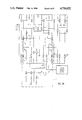
- FIG. 1 is a block diagram of a system for generating a stressed data window in accordance with the principles of the present invention.
- FIG. 2A is a schematic diagram of a VCO circuit modified for use in the system of FIG. 1.
- FIG. 2B is a schematic diagram of one part of the blocked data window generator circuit for use in the system of FIG. 1.
- FIG. 2C is a schematic diagram of another part of the blocked data window generator circuit for use in the system of FIG. 1.
- FIG. 2D is a schematic diagram of the stressed data window gate circuit for use in the system of FIG. 1.
- FIG. 3 is a timing diagram of the signal waveform produced at node N of the circuit of FIG. 2.
- FIG. 4 is a timing diagram of the signal waveforms produced at nodes Q and Z of the circuit of FIG. 2.
- FIG. 5 is a timing diagram of the signal waveforms of FIGS. 3 and 4, together with signal waveforms produced by the circuits of FIGS. 2B and FIG. 2C.
- FIG. 6 is a timing diagram of the stressed data window and related waveforms generated by the system of FIG. 1.
- phase-lock loop 9 comprises phase discriminator 11, which provides phase difference between incoming data and the feedback clock produced by VCO and clock driver 16 and provides reshaped data pulses.
- Charge pump 12 charges or discharges filter 13 in response to signals from phase discriminator 11.
- Filter 13 provides required phase-lock loop stability.
- Buffer amplifier 14 provides low impedance driving capability for signals received from filter 13 to VCO and clock driver 16.
- VCO and clock driver 16 includes a voltage controlled oscillator (VCO) 15 and related driver circuits.
- phase-lock loop 9 is similar to such loops described in "Analog Integrated Circuit Design" by Alan B. Grebene, Van Nostand Reinhold Company, 1972, pp. 298-326.
- Blocked data window generator 17 includes circuitry shown in FIGS. 2B and 2C for generating the data blocking signals used to control stress data window gate 18 for deriving the stressed data window.
- the circuit for stress data window gate 18 shown in FIG. 2D produces logic control signals for generating data standardized to clock (DSTC) signals which is not part of the present invention.
- Phase-lock loop (PLL) 9 receives input data bits to which it becomes locked. Signals produced by VCO and clock driver 15 are thus unambiguously defined by such bits for as long as data is received.
- Blocked data window generator 17 provides controlled signals when gated with the reshaped data signals from phase discriminator 11 to selectively accept data which falls within the stressed data window and reject all which do not. Thus, the smaller the stressed data window, the higher the data detection error rate and conversely.
- the reshaped data signals provided by phase discriminator 11 have constant pulse width and are derived as part of the phase discrimination process.
- VCO 15 comprises a conventional VCO circuit modified by addition of data window stressing circuit 22 as shown in FIG. 2.
- the VCO 15 produces output signals conventionally in the same manner as such circuits described in "Analog Integrated Circuit Design" by Alan B. Grebene, Van Nostand Reinhold Company, 1972, pp. 313-315.
- transistors T1 and T3 form an emitter follower stage to transistor T6 such that the voltage at node N follows the voltage at node A.
- transistors T2 and T3 form a corresponding emitter follower stage to transistor T7 such that the voltages at nodes Q and Z follow the voltage at node B.
- Resistor R1 is actively trimmed for symmetry of the stressed data window within the full data window which, in turn, is determined by the system clock frequency.
- Resistor R6 is passively trimmed to a nominal value.
- R7 is actively trimmed for the desired VCO center frequency when terminal 25 is grounded.
- V e the feedback error voltage from buffer amplifier 14, is applied at terminal 25 to vary the VCO output signal frequency in accordance with the relation
- Actively trimmed refers to adjusting the value of the resistors while observing waveforms produced by an operating circuit. “Passively trimmed” resistors are adjusted to a fixed value while the circuit is inoperative.
- Adjustment of the current at the emitter of transistor T5 controls the width of the stressed data window with respect fo full data window width. After R1 is appropriately trimmed, the voltage difference between the voltage at node N and the voltage at node Q (or at node Z) can be linearly varied by selectively controlling the current flowing in the emitter of transistor T5.
- Peak-to-peak voltage VT is the sum of voltages VD and VU.
- VD represents the capacitive regeneration at node B required for conventional operation of VCO 15 which the voltage node A tries to follow.
- Voltage VU represents capacitive boost developed at node A.
- Voltage level N 1 which is offset from the voltage level at node A by an amount approximately equal to V BE -I 3 R 4 , is the DC voltage of waveform N when the charging current for capacitor C is from node A to node B.
- VD is greater than VU owing to leakage through transistors 6 and 7, and ⁇ V is the difference between VD and VU, thus
- waveforms Q and Z represent the voltage waveforms at nodes Q and Z, respectively.
- the voltage levels Q1 and Z1 which are offsets from the DC voltage level at node B by amounts equal to -V BE -(I 1 +I 2 ) R 2 and -V BE -(I 1 +I 2 ) R 2 -I 1 R 3 , respectively, are the DC voltages of their respective waveforms when the charging current to capacitor C is from node B to node A.
- FIG. 5 shows the timing relationship of the signals of FIGS. 3 and 4 during operation of the circuits of FIGS. 2A, 2B and 2C to produce the stressed data window of the present invention.
- Waveforms WS and WR of FIG. 5 are produced by the circuit of FIG. 2B in response to waveforms N, Q and Z.
- Inputs T 1 , T 3 and T 1 , T 3 are the differential signals that determine when the system is operating in stressed data window mode.
- signal T1 (T3) is “high” and T1 (T3) “low”.
- Signal WS is “high” and WS “low” only when node N is at higher voltage than node Q.
- signal WR is “high” and WR “low” only when node Z is at higher voltage than node N.
- Waveform W of FIG. 5 is produced by the circuit of FIG. 2C in response to waveforms WS, WS, WR and WR.
- the circuit is a latch circuit.
- the trickle bias suppresses the effects of transient signals on operation of the circuit.
- the width of waveform W which is directly related to the stressed data window, is less than the width of a full data window or one cycle of system clock signal CL.
- the width of waveform W can be continuously varied by changing the offset, ⁇ M, between waveform N on the one hand and waveform Q and Z on the other.
- Offset ⁇ X the difference in DC voltage level between waveforms Q and Z is constant, being fixed by the value of resistors R1 and R3 through which current I 1 flows.
- the pulse width of waveform W is varied by changing the offset ⁇ M.
- Offset ⁇ M is changed by varying the DC level at nodes Q and Z with respect to the DC level at node N.
- the relative DC voltage level at nodes Q and Z are set by adjusting the value of R1.
- Adjusting ⁇ M provides continuous control of the width of the stressed data window.
- adjustment of ⁇ M is provided by stress window control signal 27 at the emitter of transistor T5.
- Control signal 27 is derived from a conventional current digital-to-analog converter (DAC), such as an HP model 3497A Data Acquisition Control Unit, manufactured by Hewlett-Packard Co., Palo Alto, Calif.
- DAC digital-to-analog converter
- reshaped input data is combined with the blocked data window signal (i.e. waveform W) to selectively accept or block a data bit. If the data bit is accepted, control signals to produce corresponding DSTC pulses will result. Conversely, if a data bit is blocked, no corresponding DSTC signal results.
- the blocking effect requires constant pulse width of input data pulses. As mentioned elsewhere in this specification, such constant pulse width is produced by phase discriminator 11 as part of its normal operation.
- DSTC pulses are generated in response to GD signals produced by stressed data window gate 18. Generation of DSTC pulses forms no part of the present invention.
- a circuit for stressed data window gate 18 is shown in FIG. 2D for producing logic control signals in response to reshaped data pulse RD and waveform W.
- the output GD will go “high” and RD is accepted. If the overlap between the RD and W signals is less than WT, then GD will remain “low” and RD is blocked.
- width PW of data pulse A is greater than WT and overlaps waveform W at the time data pulse A arrives, then the leading edge of data pulse A will define the leading edge of the stressed data window.
- leading edge of data pulse B defines the trailing edge of the stressed data window of PW is greater then WT and overlaps waveform W as shown.
- the pulse width of data pulses A and B are equal for symmetry. Since the system of the present invention would interpret a wider pulse width of data pulse A, such as PW', as falling in two consecutive windows, the following relation must be imposed
- WT is the minimum overlap of RD and W
- ⁇ WB min is the minimum data blocking interval
- the voltage and time of waveforms Q, Z and N are linearly related.
- the time difference between the leading edge of the clock window boundary and the leading edge of data pulse A namely, ⁇ A
- the time difference between the trailing edge of the clock window boundary and the leading edge of data pulse B namely, ⁇ B.
- Data pulses A and B are reshaped data pulses RD at two different instants of time which overlap waveform W by WT just enough to trigger the stress data window logic.
- D is the delay of latches comprising the circuit of FIG. 2C in which equal delays have been assumed for "set” and “reset” transitions
- k is a constant representing the slope of the charging/discharging rate of capacitor C.
- the stress data window may be trimmed to be symmetrical with respect to the full data window by adjusting the value of R1 to control current I 1 . Stress data window symmetry will remina independent of current I 2 .
- ⁇ M is given by
- the percent reduction of the full data window achieved for the stressed data window produced by the present invention may be computed as follows: ##EQU1##
- Percent data window reduction is therefore linearly proportional to the control current I 2 .
- Symmetry is achieved by actively trimming resistor R1 of FIG. 2. Referring now to FIG. 5, this trimming will alter the DC offset ⁇ x, between waveforms Q and Z. For a constant current level of I 2 , it is precisely the ability to alter the value of ⁇ x that provides a degree of freedom by external control for symmetry.
- the stressed data window of the present invention is formed within the full data window by symmetrically blocking RD at either end thereof. RD is blocked when the ⁇ WB min portion of W overlaps RD and is combined by stress data window gate 18. Unblocked data, GD, therefore, represents the stressed data falling within the stressed data window. Such stressed data, in turn, provides the basis for correlating data detection error rate with data window width and data bit distribution within the data window.
Landscapes
- Engineering & Computer Science (AREA)
- Signal Processing (AREA)
- Signal Processing For Digital Recording And Reproducing (AREA)
- Digital Magnetic Recording (AREA)
- Detection And Prevention Of Errors In Transmission (AREA)
- Measuring Pulse, Heart Rate, Blood Pressure Or Blood Flow (AREA)
- Arrangements For Transmission Of Measured Signals (AREA)
- Stabilization Of Oscillater, Synchronisation, Frequency Synthesizers (AREA)
Priority Applications (4)
| Application Number | Priority Date | Filing Date | Title |
|---|---|---|---|
| US06/857,897 US4726022A (en) | 1986-04-30 | 1986-04-30 | Method and apparatus for stressing the data window in magnetic storage devices |
| EP87105369A EP0244665B1 (fr) | 1986-04-30 | 1987-04-10 | Appareil et méthode de mesure de l'erreur de détection de données |
| DE3751392T DE3751392T2 (de) | 1986-04-30 | 1987-04-10 | Gerät und Methode zur Gewinnung des Datenerkennungsfehlers. |
| JP62100219A JP2503009B2 (ja) | 1986-04-30 | 1987-04-24 | デ−タ検出エラ−率測定装置 |
Applications Claiming Priority (1)
| Application Number | Priority Date | Filing Date | Title |
|---|---|---|---|
| US06/857,897 US4726022A (en) | 1986-04-30 | 1986-04-30 | Method and apparatus for stressing the data window in magnetic storage devices |
Publications (1)
| Publication Number | Publication Date |
|---|---|
| US4726022A true US4726022A (en) | 1988-02-16 |
Family
ID=25326980
Family Applications (1)
| Application Number | Title | Priority Date | Filing Date |
|---|---|---|---|
| US06/857,897 Expired - Fee Related US4726022A (en) | 1986-04-30 | 1986-04-30 | Method and apparatus for stressing the data window in magnetic storage devices |
Country Status (4)
| Country | Link |
|---|---|
| US (1) | US4726022A (fr) |
| EP (1) | EP0244665B1 (fr) |
| JP (1) | JP2503009B2 (fr) |
| DE (1) | DE3751392T2 (fr) |
Cited By (17)
| Publication number | Priority date | Publication date | Assignee | Title |
|---|---|---|---|---|
| US5067128A (en) * | 1988-09-30 | 1991-11-19 | Kabushiki Kaisha Toshiba | Recorded data reading system |
| US5109304A (en) * | 1989-12-04 | 1992-04-28 | Maxtor Corporation | Method of apparatus for detecting defects in data apparatus such as magnetic storage apparatus |
| US5258877A (en) * | 1992-04-16 | 1993-11-02 | Vtc Inc. | Data separator having a restart circuit |
| US5260842A (en) * | 1992-04-16 | 1993-11-09 | Vtc Inc. | Data separator having an accurate delay circuit |
| US5278702A (en) * | 1991-04-12 | 1994-01-11 | Western Digital Corporation | Data synchronizer with symmetric window generation |
| US5402274A (en) * | 1988-03-30 | 1995-03-28 | Hitachi, Ltd. | Data separator and signal processing circuit with an adjustable window |
| US5422896A (en) * | 1993-02-24 | 1995-06-06 | Nec Corporation | Timing check circuit for a functional macro |
| US5442492A (en) * | 1993-06-29 | 1995-08-15 | International Business Machines Corporation | Data recovery procedure using DC offset and gain control for timing loop compensation for partial-response data detection |
| US5463631A (en) * | 1990-11-07 | 1995-10-31 | Fujitsu Limited | Error pulse width expanding circuit |
| US5570243A (en) * | 1993-06-22 | 1996-10-29 | Fujitsu Limited | Variable delay circuit including current mirror and ramp generator circuits for use in the read channel of a data storage device |
| US5625506A (en) * | 1994-06-17 | 1997-04-29 | International Business Machines Corporation | Method and apparatus for reducing readback errors by controlling the phase locked loop |
| US5867332A (en) * | 1992-06-22 | 1999-02-02 | Fujitsu Limited | Window margining apparatus with delayed read data single shot (DRDSS) circuit for adjustably delaying a data pulse reproduced from a data storage device |
| US6628173B2 (en) * | 2001-12-20 | 2003-09-30 | Conexant Systems, Inc. | Data and clock extractor with improved linearity |
| US20040095194A1 (en) * | 2002-11-14 | 2004-05-20 | Gupta Atul K. | Dynamically trimmed voltage controlled oscillator |
| US20050154797A1 (en) * | 2003-11-20 | 2005-07-14 | International Business Machines Corporation | Method, apparatus, and program for detecting sequential and distributed path errors in MPIO |
| US20150127998A1 (en) * | 2013-11-07 | 2015-05-07 | Stmicroelectronics International N.V. | System and Method for Improving Memory Performance and Identifying Weak Bits |
| US20160065316A1 (en) * | 2014-08-28 | 2016-03-03 | Fujitsu Limited | Signal recovery circuit and signal recovery method |
Families Citing this family (4)
| Publication number | Priority date | Publication date | Assignee | Title |
|---|---|---|---|---|
| JP2656812B2 (ja) * | 1988-10-12 | 1997-09-24 | キヤノン株式会社 | トラッキング制御装置 |
| DE69025269T2 (de) * | 1989-11-16 | 1996-07-04 | Canon Kk | Informationsverarbeitungsgerät |
| CN101170398B (zh) * | 2007-11-30 | 2010-04-14 | 北京卫星信息工程研究所 | 一种基于压控晶体振荡器的大动态范围的快速时钟恢复系统 |
| CN101820340A (zh) * | 2010-02-22 | 2010-09-01 | 中兴通讯股份有限公司 | 一种时钟恢复装置及方法 |
Citations (4)
| Publication number | Priority date | Publication date | Assignee | Title |
|---|---|---|---|---|
| US4394695A (en) * | 1981-02-02 | 1983-07-19 | Sharp Corporation | Method and apparatus for evaluating recording systems |
| US4417286A (en) * | 1981-07-31 | 1983-11-22 | Ncr Corporation | Data window expander circuit in a data recovery system |
| US4459623A (en) * | 1982-01-18 | 1984-07-10 | Mds Qantel Corporation | Method and apparatus for recovering NRZ information from MFM data |
| US4578721A (en) * | 1984-09-10 | 1986-03-25 | Seagate Technology | Stress test for magnetic disc recording apparatus |
Family Cites Families (5)
| Publication number | Priority date | Publication date | Assignee | Title |
|---|---|---|---|---|
| JPS4956602A (fr) * | 1972-09-29 | 1974-06-01 | ||
| US4065796A (en) * | 1976-09-22 | 1977-12-27 | Hewlett-Packard Company | Digital data decoder |
| US4393458A (en) * | 1980-02-06 | 1983-07-12 | Sperry Corporation | Data recovery method and apparatus using variable window |
| JPS58133615A (ja) * | 1982-02-03 | 1983-08-09 | Nec Corp | デ−タ読出装置 |
| JPS5930217A (ja) * | 1982-08-06 | 1984-02-17 | インタ−ナシヨナル ビジネス マシ−ンズ コ−ポレ−シヨン | 誤り検出機能を有する復調器 |
-
1986
- 1986-04-30 US US06/857,897 patent/US4726022A/en not_active Expired - Fee Related
-
1987
- 1987-04-10 EP EP87105369A patent/EP0244665B1/fr not_active Expired - Lifetime
- 1987-04-10 DE DE3751392T patent/DE3751392T2/de not_active Expired - Fee Related
- 1987-04-24 JP JP62100219A patent/JP2503009B2/ja not_active Expired - Lifetime
Patent Citations (4)
| Publication number | Priority date | Publication date | Assignee | Title |
|---|---|---|---|---|
| US4394695A (en) * | 1981-02-02 | 1983-07-19 | Sharp Corporation | Method and apparatus for evaluating recording systems |
| US4417286A (en) * | 1981-07-31 | 1983-11-22 | Ncr Corporation | Data window expander circuit in a data recovery system |
| US4459623A (en) * | 1982-01-18 | 1984-07-10 | Mds Qantel Corporation | Method and apparatus for recovering NRZ information from MFM data |
| US4578721A (en) * | 1984-09-10 | 1986-03-25 | Seagate Technology | Stress test for magnetic disc recording apparatus |
Non-Patent Citations (2)
| Title |
|---|
| "Effect of Bitshift Distribution on Error Rate in Magnetic Recording" by Eric R. Katz et al, IEEE Transactions on Magnetics, vol. MAG-15, #3, May 1979. |
| Effect of Bitshift Distribution on Error Rate in Magnetic Recording by Eric R. Katz et al, IEEE Transactions on Magnetics, vol. MAG 15, 3, May 1979. * |
Cited By (22)
| Publication number | Priority date | Publication date | Assignee | Title |
|---|---|---|---|---|
| US5402274A (en) * | 1988-03-30 | 1995-03-28 | Hitachi, Ltd. | Data separator and signal processing circuit with an adjustable window |
| US5559645A (en) * | 1988-03-30 | 1996-09-24 | Hitachi, Ltd. | Disk recording apparatus with adaptive window adjusting |
| US5067128A (en) * | 1988-09-30 | 1991-11-19 | Kabushiki Kaisha Toshiba | Recorded data reading system |
| US5109304A (en) * | 1989-12-04 | 1992-04-28 | Maxtor Corporation | Method of apparatus for detecting defects in data apparatus such as magnetic storage apparatus |
| US5463631A (en) * | 1990-11-07 | 1995-10-31 | Fujitsu Limited | Error pulse width expanding circuit |
| US5278702A (en) * | 1991-04-12 | 1994-01-11 | Western Digital Corporation | Data synchronizer with symmetric window generation |
| US5258877A (en) * | 1992-04-16 | 1993-11-02 | Vtc Inc. | Data separator having a restart circuit |
| US5260842A (en) * | 1992-04-16 | 1993-11-09 | Vtc Inc. | Data separator having an accurate delay circuit |
| US5867332A (en) * | 1992-06-22 | 1999-02-02 | Fujitsu Limited | Window margining apparatus with delayed read data single shot (DRDSS) circuit for adjustably delaying a data pulse reproduced from a data storage device |
| US5422896A (en) * | 1993-02-24 | 1995-06-06 | Nec Corporation | Timing check circuit for a functional macro |
| US5570243A (en) * | 1993-06-22 | 1996-10-29 | Fujitsu Limited | Variable delay circuit including current mirror and ramp generator circuits for use in the read channel of a data storage device |
| US5442492A (en) * | 1993-06-29 | 1995-08-15 | International Business Machines Corporation | Data recovery procedure using DC offset and gain control for timing loop compensation for partial-response data detection |
| US5625506A (en) * | 1994-06-17 | 1997-04-29 | International Business Machines Corporation | Method and apparatus for reducing readback errors by controlling the phase locked loop |
| US6628173B2 (en) * | 2001-12-20 | 2003-09-30 | Conexant Systems, Inc. | Data and clock extractor with improved linearity |
| US20040095194A1 (en) * | 2002-11-14 | 2004-05-20 | Gupta Atul K. | Dynamically trimmed voltage controlled oscillator |
| US6778024B2 (en) | 2002-11-14 | 2004-08-17 | Gennum Corporation | Dynamically trimmed voltage controlled oscillator |
| US20050154797A1 (en) * | 2003-11-20 | 2005-07-14 | International Business Machines Corporation | Method, apparatus, and program for detecting sequential and distributed path errors in MPIO |
| US7076573B2 (en) * | 2003-11-20 | 2006-07-11 | International Business Machines Corporation | Method, apparatus, and program for detecting sequential and distributed path errors in MPIO |
| US20150127998A1 (en) * | 2013-11-07 | 2015-05-07 | Stmicroelectronics International N.V. | System and Method for Improving Memory Performance and Identifying Weak Bits |
| US9543044B2 (en) * | 2013-11-07 | 2017-01-10 | Stmicroelectronics International N.V. | System and method for improving memory performance and identifying weak bits |
| US20160065316A1 (en) * | 2014-08-28 | 2016-03-03 | Fujitsu Limited | Signal recovery circuit and signal recovery method |
| US9680631B2 (en) * | 2014-08-28 | 2017-06-13 | Fujitsu Limited | Signal recovery circuit and signal recovery method |
Also Published As
| Publication number | Publication date |
|---|---|
| DE3751392T2 (de) | 1996-03-07 |
| EP0244665A2 (fr) | 1987-11-11 |
| JPS62266776A (ja) | 1987-11-19 |
| EP0244665A3 (fr) | 1992-07-01 |
| EP0244665B1 (fr) | 1995-07-05 |
| JP2503009B2 (ja) | 1996-06-05 |
| DE3751392D1 (de) | 1995-08-10 |
Similar Documents
| Publication | Publication Date | Title |
|---|---|---|
| US4726022A (en) | Method and apparatus for stressing the data window in magnetic storage devices | |
| US6856206B1 (en) | Method and apparatus for acquiring a frequency without a reference clock | |
| JP3176331B2 (ja) | Pll回路 | |
| EP1095457B1 (fr) | Procede d'accord de la largeur de bande d'une boucle a phase asservie | |
| US4872155A (en) | Clock generator circuit and a synchronizing signal detection method in a sampled format system and a phase comparator circuit suited for generation of the clock | |
| US4942370A (en) | PLL circuit with band width varying in accordance with the frequency of an input signal | |
| US4740736A (en) | Servo data decoder for any amplitude dependent servo data encoding scheme | |
| US4626933A (en) | Method and apparatus for qualifying data | |
| JPS62157377A (ja) | 異なる時間で入力信号をサンプリングするための装置 | |
| US4876699A (en) | High speed sampled data digital phase detector apparatus | |
| JPS61182320A (ja) | 位相検出器および位相ロツクループ装置 | |
| US5969894A (en) | Method for detecting data encoded as state transitions in a read signal | |
| US4642562A (en) | Phase difference demodulator | |
| US5329560A (en) | AGC circuit with non-linear gain for use in PLL circuit | |
| CN100334807C (zh) | 相位误差确定方法和数字锁相环系统 | |
| EP0572161B1 (fr) | CÔntrole automatique et non-linéaire du gain pour circuits à boucle à verrouillage de phase | |
| JP2567546B2 (ja) | 2値データ記録システム | |
| JP3357208B2 (ja) | 同期信号発生装置 | |
| US5793825A (en) | Method and apparatus for extending an operating frequency range of an instantaneous phase-frequency detector | |
| US20040088619A1 (en) | Method and apparatus for enabling fast clock phase locking in a phase-locked loop | |
| JPS6363135B2 (fr) | ||
| EP0190578B1 (fr) | Discriminateur de phase pour une horloge | |
| US4698600A (en) | Clock phase discriminator | |
| JPS61177814A (ja) | 位相弁別器 | |
| JPH087468A (ja) | 光ディスク再生装置 |
Legal Events
| Date | Code | Title | Description |
|---|---|---|---|
| AS | Assignment |
Owner name: INTERNATIONAL BUSINESS MACHINES CORPORATION, NEW Y Free format text: ASSIGNMENT OF ASSIGNORS INTEREST;ASSIGNORS:CHAN, PATRICK MENG-HO;CHEN, SHIN C.;SIGNING DATES FROM 19860430 TO 19860512;REEL/FRAME:004548/0916 Owner name: INTERNATIONAL BUSINESS MACHINES CORPORATION, ARMON Free format text: ASSIGNMENT OF ASSIGNORS INTEREST.;ASSIGNORS:CHAN, PATRICK MENG-HO;CHEN, SHIN C.;REEL/FRAME:004548/0916;SIGNING DATES FROM 19860430 TO 19860512 |
|
| FPAY | Fee payment |
Year of fee payment: 4 |
|
| FPAY | Fee payment |
Year of fee payment: 8 |
|
| REMI | Maintenance fee reminder mailed | ||
| LAPS | Lapse for failure to pay maintenance fees | ||
| FP | Lapsed due to failure to pay maintenance fee |
Effective date: 20000216 |
|
| STCH | Information on status: patent discontinuation |
Free format text: PATENT EXPIRED DUE TO NONPAYMENT OF MAINTENANCE FEES UNDER 37 CFR 1.362 |