US4714875A - Printed circuit board fault location system - Google Patents
Printed circuit board fault location system Download PDFInfo
- Publication number
- US4714875A US4714875A US06/722,406 US72240685A US4714875A US 4714875 A US4714875 A US 4714875A US 72240685 A US72240685 A US 72240685A US 4714875 A US4714875 A US 4714875A
- Authority
- US
- United States
- Prior art keywords
- circuit board
- connector
- pins
- recess
- housing
- Prior art date
- Legal status (The legal status is an assumption and is not a legal conclusion. Google has not performed a legal analysis and makes no representation as to the accuracy of the status listed.)
- Expired - Fee Related
Links
Images


Classifications
-
- G—PHYSICS
- G01—MEASURING; TESTING
- G01R—MEASURING ELECTRIC VARIABLES; MEASURING MAGNETIC VARIABLES
- G01R31/00—Arrangements for testing electric properties; Arrangements for locating electric faults; Arrangements for electrical testing characterised by what is being tested not provided for elsewhere
- G01R31/28—Testing of electronic circuits, e.g. by signal tracer
- G01R31/317—Testing of digital circuits
- G01R31/3181—Functional testing
- G01R31/319—Tester hardware, i.e. output processing circuits
- G01R31/31917—Stimuli generation or application of test patterns to the device under test [DUT]
- G01R31/31926—Routing signals to or from the device under test [DUT], e.g. switch matrix, pin multiplexing
-
- G—PHYSICS
- G01—MEASURING; TESTING
- G01R—MEASURING ELECTRIC VARIABLES; MEASURING MAGNETIC VARIABLES
- G01R31/00—Arrangements for testing electric properties; Arrangements for locating electric faults; Arrangements for electrical testing characterised by what is being tested not provided for elsewhere
- G01R31/26—Testing of individual semiconductor devices
- G01R31/2607—Circuits therefor
- G01R31/2637—Circuits therefor for testing other individual devices
-
- G—PHYSICS
- G01—MEASURING; TESTING
- G01R—MEASURING ELECTRIC VARIABLES; MEASURING MAGNETIC VARIABLES
- G01R31/00—Arrangements for testing electric properties; Arrangements for locating electric faults; Arrangements for electrical testing characterised by what is being tested not provided for elsewhere
- G01R31/28—Testing of electronic circuits, e.g. by signal tracer
- G01R31/317—Testing of digital circuits
- G01R31/3181—Functional testing
- G01R31/319—Tester hardware, i.e. output processing circuits
- G01R31/31903—Tester hardware, i.e. output processing circuits tester configuration
- G01R31/31907—Modular tester, e.g. controlling and coordinating instruments in a bus based architecture
-
- G—PHYSICS
- G01—MEASURING; TESTING
- G01R—MEASURING ELECTRIC VARIABLES; MEASURING MAGNETIC VARIABLES
- G01R31/00—Arrangements for testing electric properties; Arrangements for locating electric faults; Arrangements for electrical testing characterised by what is being tested not provided for elsewhere
- G01R31/28—Testing of electronic circuits, e.g. by signal tracer
- G01R31/317—Testing of digital circuits
- G01R31/3181—Functional testing
- G01R31/319—Tester hardware, i.e. output processing circuits
- G01R31/31903—Tester hardware, i.e. output processing circuits tester configuration
- G01R31/31912—Tester/user interface
-
- G—PHYSICS
- G06—COMPUTING OR CALCULATING; COUNTING
- G06F—ELECTRIC DIGITAL DATA PROCESSING
- G06F11/00—Error detection; Error correction; Monitoring
- G06F11/22—Detection or location of defective computer hardware by testing during standby operation or during idle time, e.g. start-up testing
- G06F11/26—Functional testing
- G06F11/261—Functional testing by simulating additional hardware, e.g. fault simulation
-
- G—PHYSICS
- G06—COMPUTING OR CALCULATING; COUNTING
- G06F—ELECTRIC DIGITAL DATA PROCESSING
- G06F11/00—Error detection; Error correction; Monitoring
- G06F11/22—Detection or location of defective computer hardware by testing during standby operation or during idle time, e.g. start-up testing
- G06F11/26—Functional testing
- G06F11/273—Tester hardware, i.e. output processing circuits
- G06F11/277—Tester hardware, i.e. output processing circuits with comparison between actual response and known fault-free response
Definitions
- This invention generally concerns an improved testing apparatus and more particularly concerns a so-called in-circuit testing apparatus for the testing of electrical components assembled on a printed circuit board for example without necessitating removal or disconnection of the respective components from the printed circuit board.
- a number of different types of sophisticated and expensive systems are available for the testing of completed printed circuit board assemblies of electrical components.
- One type is adapted for functional testing by application to inputs of the powered-up printed circuit board assembly of test signals and sequences thereof formulated to enable the functional operation of the assembly to be monitored by monitoring of corresponding signals obtained from outputs and other test nodes of the assembly.
- Another type sometimes called an in-circuit tester, is adapted not so much for functional testing of the overall circuit board assembly as for the determination of manufacturing defects such as short circuits, tracking faults, mis-inserted and/or missing and/or out of tolerance components, and the function of individual integrated circuits, etc.
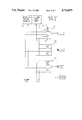
- FIGS. 1 and 2 of the accompanying drawings illustrate a known automatic fault location system.
- the system briefly comprises a central processor unit 1 which, under the control of an operator unit 2, determines the connection of selected circuit nodes of a printed circuit board under test (B.U.T.) through an adapter 3 and a scanner switching matrix array 4 to a measuring unit 5.
- the adapter 3 comprises any convenient means such as a vacuum operated "bed-of-nails" type coupler for contacting selected circuit nodes of the B.U.T.
- the matrix array 4 comprises a multiplicity of selectively addressable switches arranged as described hereinafter with reference to FIG. 2 and enabling the connection through the adapter 3 of any of the circuit nodes of the B.U.T. with a constant current source and/or a voltage measurement device in the measuring unit 5.
- FIG. 2 illustrates the architecture of the scanner switching matrix array 4.
- a constant current source 10 and a differential voltmeter 11 constituting components of the measuring unit 5 are coupled via respective buses to a plurality of switching networks 12 each comprising four field effect transistors 13 and each providing a test point TP configurable either for current injection or for current reception in dependence upon a control input either to common connected gate 14 of FET pair 15 or to common connected gate 16 of FET pair 17 respectively.
- a control input might be applied to gate 14 of FET pair 15 of switching network 12 1 associated with TP1 so as to configure TP1 as a current injection node, and a control input might be applied to gate 16 of FET pair 17 of switching network 12 2 associated with TP2 so as to configure TP2 as a current reception node.
- a current derived from current source 10 can then be applied through the resistor connected between TP1 and TP2, and the voltage developed across the resistor measured by means of voltmeter 11 coupled to TP1 and TP2 via the lower FET of FET pair 15 associated with network 12 1 and the upper FET of FET pair 17 associated with network 12 2 respectively.
- the central processing unit 1 has the task, inter alia, of setting the control inputs to the gates of the FET pairs 15,17 in conjunction with timing the operations of the measuring unit 5, it being appreciated that the overall system function is essentially digital.
- a resistor may be measured by injection of a current pulse and measuring the resultant voltage
- a capacitor may similarly be measured by measurement of the voltage to which the capacitor charges in response to the application of a current pulse for a determined time period.
- the viability of diodes and the inter-electrode characteristics of transistors can also be checked, as can also the viability of components in parallel and series-parallel resistor, capacitor and diode combinations by appropriate selection of current pulse characteristics (amplitude and duration particularly) and of measurement timings.
- the printed circuit board under test is powered-down in the course of the test so that the function of the overall board assembly is not being tested, but rather the viability and the in-tolerance value acceptability of individual and collective components on the board is tested.
- a fault location system for testing the viability of components on a printed circuit board or the like comprises a matrix array of bidirectionally current conducting analog switching networks each defining a test point for connection to a node of a board under test and connectable by control of the switching network either to a stimulus source or to a reference (e.g. ground) potential and simultaneously to a corresponding input of a measurement facility.
- the fault location system according to the present invention is further characterised in relation to the prior art in that it advantageously comprises means enabling a plurality of stimulus sources to be selectively connected to the array of switching networks.
- a current source has been provided which is pulsed to provoke a voltage measurement
- both AC and DC current and voltage sources can be utilised to determine circuit board and component conditions.
- the analog switching networks each preferably comprise four bidirectional analog transmission gates which could be configured as discrete field effect transistor circuits but preferably are in integrated circuit form.
- the four bidirectional analog transmission gates are commonly connected at one side to define the test point of the respective switching network and at their other sides define four terminals which constitute the input/output terminals of the network.
- the control terminals of the four analog transmission gates are preferably connected together to define two control terminals for the network so that by application of an appropriate input to a respective one of the two network control terminals a respective two of the bidirectional analog transmission gates will be switched into conduction so as to connect the test point of the network firstly to the stimulus source and secondly to a respective input of the measurement facility. If the other of the network control terminals is addressed with an appropriate input, then conversely the test point of the network will be connected to ground and to a different input of the measurement facility.
- the switching networks constructed of four bidirectional analog transmission gates thus will be appreciated to comprise four terminals each selectively connectable to a respective one of a stimulus source, a reference potential and two measurement nodes, a test point selectively connectable either to the stimulus source and a first of the measurement nodes or to the reference source and a second of the measurement nodes, and two network control terminals which determine which of the two different test point connections available through the network are realised.
- an apparatus for testing circuit boards for manufacturing defects comprising a main body part and a plug-in-module removably insertable into the main body part, an interface connector comprising a pin matrix array mounted on the plug-in module and a connector matrix array mounted on the main body part providing for a plurality of connections between the plug-in module and the main body part, a circuit board receiving surface of the plug-in module having associated therewith a plurality of probes for simultaneously probing selected circuit nodes of a circuit board received thereon, and connections being provided between said probes and respective ones of the pins of said pin matrix array.
- FIG. 3 is a schematic representation of a bidirectional switching network as employed in the system according to the present invention.
- FIG. 4 is a more detailed showing of the network array of FIG. 3 depicted in a manner similar to the showing in FIG. 2 of the aforedescribed prior art system;
- FIG. 5 is a partial circuit diagram of an exemplary embodiment of the invention.
- FIG. 6 shows a modification of the circuit diagram of FIG. 5
- FIG. 7 is a schematic block diagram which illustrates the testing philosophy of the embodiments of FIGS. 5 and 6;
- FIG. 8 schematically illustrates a possible physical arrangement of an automatic fault location system according to the present invention.
- FIG. 9 is a schematic sectional view taken on the line IX . . . IX in FIG. 8.
- FIG. 3 which schematically illustrates a bidirectional switching network utilised in the performance of the invention
- the network will be seen to comprise four bidirectional switches designated 31, 32, 33 and 34 interconnected as shown with each other and with source +, source -, test point (node) and two separate measurement terminals designated 35 to 39 respectively.
- Control terminals 40 and 41 also are provided respectively for determining the operation of the switches 31 and 32 and the switches 33,34.
- switches 31 and 32 can be rendered conductive so as to connect test point (node) 37 to the stimulation source +terminal 35 and to the "positive" measurement terminal 38.
- switches 33 and 34 are enabled to connect the test point (node) 37 to the source -terminal 36 and to the "negative" measurement terminal 39.
- the network shown in FIG. 3 is but one of a large number of parallel-connected networks each individually addressable via its control terminals to connect its respective test point (node) either to the stimulus source +terminal 35 and to measurement terminal 38 or to the source -(reference) terminal 36 and to measurement terminal 39.
- a component on a printed circuit board for example a resistor whose resistance is to be verified as being within specified tolerances of its nominal value, can be contacted at one of its ends by means of a probe coupled to the test point (node) of any one switching network and can be contacted at its other end by means of a probe coupled to the test point (node) of any other switching network, and the two switching networks in question can be controlled by appropriate addressing of their control terminals so that one test point (node) coupled to one end of the resistor is coupled to the stimulus source (for example a constant current generator) and to one terminal of a voltage measurement device and the other test point (node) coupled to the other end of the resistor is coupled to ground and to another terminal of the voltage measurement device.
- the stimulus source for example a constant current generator
- a current pulse supplied from the stimulus source to ground via the resistor will set up a corresponding voltage across the resistor which can be measured by the voltage measurement device to enable the resistance value of the resistor to be computed and, as desired, compared with its nominal value to enable a decision to be taken as to whether or not its resistance value is within an acceptable tolerance range of the nominal value.
- the addressing of the control terminals of the switching networks, the timing and the nature of the stimulus applications and of the measurements may advantageously be under computer control so that a multiplicity of components in a printed circuit board for example may be tested automatically in accordance with a preprogrammed routine.
- FIG. 4 shows, in a manner similar to the showing in FIG. 2 of a prior art switching network, the actual make-up of the switching network of FIG. 3 and the same reference numerals are used in FIG. 4 as are used to designate like parts in FIG. 3.
- each of the switches 31,32,33,34 comprises a bidirectional analog transmission gate, and the four gates are connected as shown to define two control terminals 40 and 41 coupled via inverters to the gate electrodes of respective pairs of the gates 31,32,33,34.
- FIG. 5 shows the general circuit arrangement of an exemplary system according to the present invention.
- Reference numeral 51 designates a multiplexer comprising a plurality of the switching networks described above with reference to FIGS. 3 and 4, the multiplexer 51 having associated therewith address buses designated 40' and 41' for computer controlled addressing of the control terminals 40 and 41 of the switching networks and further having terminals 35',36',38', and 39' corresponding respectively to the source +terminal 35, the source -(reference) terminal 36, and the respective measurement terminals 38 and 39 of the switching networks.
- the source terminal 35' is selectively connectable via a switching device 52 controllable from the central processing unit (not shown) of the system with voltage, current and frequency sources 53, 54 and 55 respectively all comprising integral parts of the system, and with an external terminal.
- a standard resistor 56 in the voltage source line enables high value resistors to be measured.
- the measurement terminals 38', 39' of the multiplexer 51 are coupled to an instrumentation amplifier generally designated 57 comprising high impedance buffers 58 and a differential amplifier 59, and the output of the instrumentation amplifier 57 is coupled via a two way switch 66 to a window comparator arrangement 60 for comparison with "high” and “low” reference levels V H and V L in order to provide corresponding inputs to logical circuitry 61 providing "high", “in” or “low” outputs representative of the relationship of the measured value of the component in question to a predetermined tolerance range associated with an acceptable component.
- the output of the instrumentation amplifier 57 is also applied to a display databus 62 via an analog-to-digital converter 63 fed via a switching device 64 controllable from the central processing unit with either the direct output of the instrumentation amplifier 57 or with the output of an RMS-DC converter 65.
- the switch 64 is also connected to receive a signal representative of the voltage V i derived across test resistor 56 aforementioned in order to measure source currents.
- a digital-to-analog converter 67 enables a negative reference voltage V- to be selectively applied via two way switch 68 to the reference terminal 36' of multiplexer 51, the D-A converter 67 and the switch 68 being controllable from the central processing unit of the apparatus.
- FIG. 6 shows a modification of the circuit of FIG. 5 designed to enable measurement of the gain of a discrete transistor to be effected and also to enable so-called guarding techniques to be employed in the analysis of multiple component networks.
- the outputs of the buffer amplifiers 58 of FIG. 5 are additionally applied via a selector 69 to a summing amplifier 70 for summing with the output of a digital-to-analog converter 71 in order to derive an additional stimulus signal to be applied selectively to the circuit nodes 72 by selective operation of the relays 73.
- the emitter and collector of the transistor are probed by respective ones of the circuit nodes 37 shown in FIG.
- the digital-to-analog converter 71 provides an added current value enabling the base conditions to be established for determining the gain of the transistor.
- the modified circuit arrangement of FIG. 6 also enables measurements to be made by means of a guarding technique. For example, if a resistor R1 was connected between TP1 and TP2 in FIG. 4 and series connected resistors R2 and R3 were also connected between TP1 and TP2 in parallel with resistor R1, the circuit arrangement of FIG. 5 would not enable the value of R1 alone to be determined on account of the effect of parallel connected R2 and R3. However, with the arrangement of FIG. 6 and by coupling of the junction of R2 and R3 to one of the test nodes 72 the potential can be equalised on either side of R2 (or R3) thereby effectively isolating R1 and enabling its value to be measured. In this way, resistor R1 is guarded from the effects of parallel-connected series resistors R2 and R3.
- FIG. 7 is a general representation of a system according to the present invention useful for an understanding of the philosophy underlying the inventive system.
- the multiplexer 51 above described is shown providing a plurality of measurement nodes 1,2,3 . . . N, as well as the control terminal selection input buses 40',41', and the source, reference (ground) and two measurement nodes 35',36',38' and 39' aforementioned.
- the measurement system, designated 60 responds to input data from the central processing unit (not shown) of the system regarding the measurement type (e.g.
- FIG. 8 is a perspective view of an exemplary fault location apparatus constructed in accordance with the present invention and FIG. 9 is a partial sectional view taken on the line IX . . . IX in FIG. 8.
- the apparatus is adapted for desk-top or table-top use and comprises a moulded aluminium base 80 and a moulded plastic cover 81 defining a housing formed with a central recess 82 adapted to receive a module 83 which, as will be described hereinafter, is customised for the particular circuit to be tested and has on its underside an interface connector 84 adapted to mate with a complementary connector 85 provided in the bottom of the recess 82.
- the housing defined by the base 80 and cover 81 contains the electronic circuits and other components of the apparatus and, as shown, the cover 81 has an inclined front face which serves as a mounting for a control panel 86 preferably utilising membrane type switches, a paper roll printer 87, and an LCD display 88 for displaying operator commands etc.
- a flip-up lid 89 provides access to hard and/or floppy disc drives.
- the module 83 is constructed as a rigid rectangular box of precise dimensions adapted to fit closely within the recess 82, though not so closely that the complementary connector parts 84,85 cannot adjust for precise positioning relative to each other, there being provided in the connector part 84 a pair of spaced-apart precisely formed and precisely positioned bores 90 (one of which can be seen in FIG. 9) and there being provided in the connector part 85 a correspondingly precisely located positioning member 91 (see FIG. 8) comprising a conical head portion mounted on a relatively rigid shaft mounted in an oil dash-pot. As the connector parts 84,85 are moved towards each other, the conical head of the member 91 engages in the bore 90 and thereafter guides the two connector parts into precisely controlled positional interrelationship with each other.
- reference numeral 92 designates a circuit board to be tested adapted to be received upon an insulating carrier plate 93 which is mounted in the module 83 of the apparatus by means of a flexible diaphragm 94, the carrier plate 93 being apertured correspondingly to the positions of a plurality of spring loaded probe pins 95 secured in a detachable insulating bed plate 96, the positions of the pins 95 in the plate 96 being determined in accordance with the arrangement of the circuit board 92 so that when, in response to a vaccum established within the depicted apparatus, the circuit board 90 is drawn down with flexure of the diaphragm 94 towards the bed plate 96 the pins 95 contact the circuit nodes of the printed circuit board 92.
- the arrangement for establishing the requisite vacuum within the apparatus so as to pull down the circuit board 92 onto the pins 95 is only schematically illustrated, but will be well understood by
- the pins 95 in the bed plate 96 are wire wrapped with respective connecting leads 97 coupled to selected pins of a pin matrix array formed in the first connector part 84 which comprises an insulating plastic support 98 with a plurality of rows of terminal pins or "nails" 99 mounted therein as shown with their shanks projecting from the upper surface of the support 98 and their heads flush with the under side.
- a pin matrix array formed in the first connector part 84 which comprises an insulating plastic support 98 with a plurality of rows of terminal pins or "nails" 99 mounted therein as shown with their shanks projecting from the upper surface of the support 98 and their heads flush with the under side.
- the cooperating connector part 85 comprises an insulating plastics support 100 which serves as a mounting for a connector matrix comprising a plurality of rows of connector pins 101 each with a spring-loaded head portion contactable by the head portion of a respective one of the pins 99 of the matrix array provided in connector part 84.
- the pins 101 of the connector matrix extend through correspondingly located holes of a printed circuit board 102 and are connected on the underside of the board 102 with surface mounted integrated circuit devices 103 constituting the electronic circuitry of the system as hereinbefore described with reference to FIGS. 3 to 6, and particularly the switching networks of FIG. 3, such devices being mounted directly on the board 103 between the rows of pins 101 and thus having minimal lead lengths with consequent advantages as regards minimising of stray resistance, capacitance and inductance.
- FIGS. 8 and 9 The arrangement of FIGS. 8 and 9 is particularly convenient in that the bed plate 96 and the pin matrix array of connector part 84 can readily be customised for any particular circuit board to be tested, and no other adaptation of the apparatus is required to convert the apparatus for the testing of a different circuit board, it being appreciated that the pin configuration established at the pin matrix array of connector part 84 determines the connections made at the connector matrix of connector part 85 which in turn determines which of the measurement nodes 1 to N of the multiplex switching circuit array 51 of FIGS. 5 to 7 are available for operation in the testing of any particular printed circuit board.
- FIGS. 8 and 9 utilises a vacuum for drawing the circuit board to be tested down onto the probe pins 95 and will require the provision of vacuum supply arrangements 104 and seals 105 which are schematically and exemplarily shown in FIG. 9. Whilst such a vacuum powered arrangement is preferred, nonetheless the circuit board being tested could be urged by mechanical means into contact with the probe pins.
- the present invention provides a powerful and yet cost efficient production aid.
- a manufacturing defects analyser in accordance with the present invention could be used with the automatic test equipment disclosed in our British Patent Application No. 8429657 filed 23rd Nov. 1984, the manufacturing defects analyser constituting one of the modules of the automatic test equipment.
Landscapes
- Engineering & Computer Science (AREA)
- Physics & Mathematics (AREA)
- General Physics & Mathematics (AREA)
- General Engineering & Computer Science (AREA)
- Human Computer Interaction (AREA)
- Computer Networks & Wireless Communication (AREA)
- Tests Of Electronic Circuits (AREA)
- Measuring Leads Or Probes (AREA)
- Testing Of Short-Circuits, Discontinuities, Leakage, Or Incorrect Line Connections (AREA)
Applications Claiming Priority (4)
| Application Number | Priority Date | Filing Date | Title |
|---|---|---|---|
| GB8409794 | 1984-04-16 | ||
| GB848409794A GB8409794D0 (en) | 1984-04-16 | 1984-04-16 | Testing apparatus |
| GB8508319 | 1985-03-29 | ||
| GB08508319A GB2157837B (en) | 1984-04-16 | 1985-03-29 | Circuit testing apparatus |
Publications (1)
| Publication Number | Publication Date |
|---|---|
| US4714875A true US4714875A (en) | 1987-12-22 |
Family
ID=26287620
Family Applications (1)
| Application Number | Title | Priority Date | Filing Date |
|---|---|---|---|
| US06/722,406 Expired - Fee Related US4714875A (en) | 1984-04-16 | 1985-04-12 | Printed circuit board fault location system |
Country Status (9)
| Country | Link |
|---|---|
| US (1) | US4714875A (fr) |
| EP (1) | EP0159907A3 (fr) |
| AU (1) | AU586163B2 (fr) |
| BR (1) | BR8501786A (fr) |
| CA (1) | CA1235527A (fr) |
| DK (1) | DK170585A (fr) |
| ES (1) | ES8607571A1 (fr) |
| GB (1) | GB2157837B (fr) |
| IE (1) | IE56616B1 (fr) |
Cited By (40)
| Publication number | Priority date | Publication date | Assignee | Title |
|---|---|---|---|---|
| US4857833A (en) * | 1987-08-27 | 1989-08-15 | Teradyne, Inc. | Diagnosis of faults on circuit board |
| US4908576A (en) * | 1987-09-08 | 1990-03-13 | Jackson Daniel K | System for printed circuit board testing |
| WO1990012326A1 (fr) * | 1989-04-05 | 1990-10-18 | Knights Technology, Inc. | Detection de contact pour essais de circuits integres |
| US5019771A (en) * | 1990-05-09 | 1991-05-28 | Knights Technology, Inc. | Contact sensing for integrated circuit testing |
| US5023545A (en) * | 1990-06-04 | 1991-06-11 | The United States Of America | Circuit probing system |
| US5029168A (en) * | 1989-02-27 | 1991-07-02 | Acer Incorporated | Multiplexing communication card and scanning method for run-in testing |
| US5047708A (en) * | 1988-12-23 | 1991-09-10 | Kondner Jr Robert L | Apparatus for testing circuit boards |
| US5086271A (en) * | 1990-01-12 | 1992-02-04 | Reliability Incorporated | Driver system and distributed transmission line network for driving devices under test |
| US5113140A (en) * | 1990-06-20 | 1992-05-12 | National Research Council Of Canada | Microprocessor-controlled high-voltage capacitance bridge |
| US5353243A (en) * | 1989-05-31 | 1994-10-04 | Synopsys Inc. | Hardware modeling system and method of use |
| DE4417573A1 (de) * | 1993-08-31 | 1995-03-09 | Hewlett Packard Co | System und Verfahren zum Erfassen von Kurzschlüssen, Leerläufen und verbundenen Anschlußstiften auf einer gedruckten Leiterplatte unter der Verwendung eines automatischen Testgeräts |
| US5400406A (en) * | 1993-07-06 | 1995-03-21 | Gentex Corporation | Aircraft communication headset tester |
| US5459410A (en) * | 1991-06-17 | 1995-10-17 | Photon Dynamics, Inc. | Method and apparatus for automatically inspecting and repairing an active matrix LCD panel |
| US5528137A (en) * | 1995-01-24 | 1996-06-18 | International Business Machines Corporation | Network sensitive pulse generator |
| US5541862A (en) * | 1994-04-28 | 1996-07-30 | Wandel & Goltermann Ate Systems Ltd. | Emulator and digital signal analyzer |
| US5543727A (en) * | 1994-04-05 | 1996-08-06 | Bellsouth Corporation | Run-in test system for PC circuit board |
| US5561367A (en) * | 1992-07-23 | 1996-10-01 | Xilinx, Inc. | Structure and method for testing wiring segments in an integrated circuit device |
| US5673295A (en) * | 1995-04-13 | 1997-09-30 | Synopsis, Incorporated | Method and apparatus for generating and synchronizing a plurality of digital signals |
| JP2716285B2 (ja) | 1991-06-10 | 1998-02-18 | 日本電気アイシーマイコンシステム株式会社 | デバッグ装置 |
| US5744979A (en) * | 1992-07-23 | 1998-04-28 | Xilinx, Inc. | FPGA having logic cells configured by SRAM memory cells and interconnect configured by antifuses |
| US5933019A (en) * | 1997-03-05 | 1999-08-03 | Depue; Clayton S. | Circuit board testing switch |
| US6130530A (en) * | 1997-12-22 | 2000-10-10 | Hd Electric Company | Tester for power transformers and capacitors |
| US6148275A (en) * | 1989-05-31 | 2000-11-14 | Synopsys, Inc. | System for and method of connecting a hardware modeling element to a hardware modeling system |
| US6686747B2 (en) * | 1997-03-07 | 2004-02-03 | Micron Technology, Inc. | Programmable voltage divider and method for testing the impedance of a programmable element |
| US20040080309A1 (en) * | 2002-08-30 | 2004-04-29 | Peter Schmid | Method for performing test measurements on electrical components |
| US6795743B1 (en) | 2000-09-18 | 2004-09-21 | Dell Products L.P. | Apparatus and method for electronically encoding an article with work-in-progress information |
| WO2004090560A3 (fr) * | 2003-04-10 | 2005-01-20 | Colin Barker | Ameliorations apportees a une machine d'essai automatique |
| US20050174146A1 (en) * | 2003-10-01 | 2005-08-11 | Stmicroelectronics Pvt. Ltd. | Input buffer and method of operating the same |
| US20060195276A1 (en) * | 2002-09-19 | 2006-08-31 | Marvell International Ltd. Argyle House | Configurable voltage regulator |
| US20070043987A1 (en) * | 2002-09-19 | 2007-02-22 | Sehat Sutardja | Configurable voltage regulator |
| US20070094423A1 (en) * | 2005-10-25 | 2007-04-26 | Lee Atkinson | Device recognition system and method |
| US20070126438A1 (en) * | 2005-11-30 | 2007-06-07 | Ip Leader Technology Corporation | Probing apparatus, probing circuit board and probing system for high-voltage matrix probing |
| US20110156717A1 (en) * | 2009-12-31 | 2011-06-30 | Su-Wei Tsai | Electrical connection defect detection system and method |
| US20120059611A1 (en) * | 2010-09-07 | 2012-03-08 | Hon Hai Precision Industry Co., Ltd. | Test circuit for testing flexible printed circuit |
| CN103308842A (zh) * | 2012-03-07 | 2013-09-18 | 鸿富锦精密工业(深圳)有限公司 | 调试电路 |
| US20150054515A1 (en) * | 2013-08-23 | 2015-02-26 | Samsung Display Co., Ltd. | Printed circuit board assembly and display device having the same |
| CN107688144A (zh) * | 2017-09-25 | 2018-02-13 | 河南中烟工业有限责任公司 | 一种烟机电路板故障定位装置 |
| CN111896858A (zh) * | 2020-04-30 | 2020-11-06 | 珠海博杰电子股份有限公司 | 微针电子测试系统 |
| US20200363467A1 (en) * | 2019-05-17 | 2020-11-19 | Pegatron Corporation | Electronic device, signal validator, and method for signal validation |
| CN114829958A (zh) * | 2019-12-20 | 2022-07-29 | 西门子股份公司 | 用于评估印刷电路板的方法和系统 |
Families Citing this family (11)
| Publication number | Priority date | Publication date | Assignee | Title |
|---|---|---|---|---|
| DE3441578A1 (de) * | 1984-11-14 | 1986-05-22 | Riba-Prüftechnik GmbH, 7801 Schallstadt | Leiterplatten-pruefeinrichtung |
| FR2623630B1 (fr) * | 1987-11-23 | 1992-01-03 | Lmt Radio Professionelle | Procede et dispositif de localisation des pannes de circuits logiques |
| GB8728444D0 (en) * | 1987-12-04 | 1988-01-13 | Plessey Co Plc | Analogue circuit element & chain for testing analogue circuit |
| GB9121506D0 (en) * | 1991-10-10 | 1991-11-27 | Smiths Industries Plc | Resistance monitors |
| GB2260416B (en) * | 1991-10-10 | 1995-07-26 | Smiths Industries Plc | Resistance monitors |
| GB2261957B (en) * | 1991-11-16 | 1995-05-17 | Voltech Instr Ltd | Apparatus for testing wound components |
| GB2274716A (en) * | 1992-09-22 | 1994-08-03 | Mistrock Microsystems Limited | Circuit tester |
| GB2278689B (en) * | 1993-06-02 | 1997-03-19 | Ford Motor Co | Method and apparatus for testing integrated circuits |
| DE69506274T2 (de) * | 1994-10-06 | 1999-04-22 | Northern Telecom Ltd., Montreal, Quebec | Bus für empfindliche analoge signale |
| US5861743A (en) * | 1995-12-21 | 1999-01-19 | Genrad, Inc. | Hybrid scanner for use in an improved MDA tester |
| SG11202105198XA (en) * | 2018-11-21 | 2021-06-29 | Lam Res Corp | Wireless electronic-control system |
Citations (8)
| Publication number | Priority date | Publication date | Assignee | Title |
|---|---|---|---|---|
| GB766935A (en) * | 1953-10-26 | 1957-01-30 | Ibm | Circuit testing apparatus |
| GB850061A (en) * | 1958-10-13 | 1960-09-28 | Beckman Instruments Inc | Data handling system |
| GB994220A (en) * | 1961-04-17 | 1965-06-02 | Siemens Ag | Measuring or metering devices |
| GB1263644A (en) * | 1969-08-07 | 1972-02-16 | Olivetti & Co Spa | Apparatus for automatically testing electronic circuits |
| GB1328831A (en) * | 1969-09-13 | 1973-09-05 | Hartmann & Braun Ag | Switching circuit for switching through atlernating measuring voltages in a measuring arrangement |
| US4225819A (en) * | 1978-10-12 | 1980-09-30 | Bell Telephone Laboratories, Incorporated | Circuit board contact contamination probe |
| US4342958A (en) * | 1980-03-28 | 1982-08-03 | Honeywell Information Systems Inc. | Automatic test equipment test probe contact isolation detection method |
| JPS6072317A (ja) * | 1983-09-28 | 1985-04-24 | Nec Corp | Lsi論理回路 |
Family Cites Families (5)
| Publication number | Priority date | Publication date | Assignee | Title |
|---|---|---|---|---|
| US3854125A (en) * | 1971-06-15 | 1974-12-10 | Instrumentation Engineering | Automated diagnostic testing system |
| US3851161A (en) * | 1973-05-07 | 1974-11-26 | Burroughs Corp | Continuity network testing and fault isolating |
| US4070565A (en) * | 1976-08-18 | 1978-01-24 | Zehntel, Inc. | Programmable tester method and apparatus |
| US4114093A (en) * | 1976-12-17 | 1978-09-12 | Everett/Charles, Inc. | Network testing method and apparatus |
| US4465972A (en) * | 1982-04-05 | 1984-08-14 | Allied Corporation | Connection arrangement for printed circuit board testing apparatus |
-
1985
- 1985-03-29 GB GB08508319A patent/GB2157837B/en not_active Expired
- 1985-04-10 IE IE905/85A patent/IE56616B1/xx unknown
- 1985-04-12 US US06/722,406 patent/US4714875A/en not_active Expired - Fee Related
- 1985-04-15 AU AU41325/85A patent/AU586163B2/en not_active Ceased
- 1985-04-15 CA CA000479174A patent/CA1235527A/fr not_active Expired
- 1985-04-15 ES ES542237A patent/ES8607571A1/es not_active Expired
- 1985-04-15 BR BR8501786A patent/BR8501786A/pt not_active IP Right Cessation
- 1985-04-16 DK DK170585A patent/DK170585A/da active IP Right Grant
- 1985-04-16 EP EP85302670A patent/EP0159907A3/fr not_active Withdrawn
Patent Citations (8)
| Publication number | Priority date | Publication date | Assignee | Title |
|---|---|---|---|---|
| GB766935A (en) * | 1953-10-26 | 1957-01-30 | Ibm | Circuit testing apparatus |
| GB850061A (en) * | 1958-10-13 | 1960-09-28 | Beckman Instruments Inc | Data handling system |
| GB994220A (en) * | 1961-04-17 | 1965-06-02 | Siemens Ag | Measuring or metering devices |
| GB1263644A (en) * | 1969-08-07 | 1972-02-16 | Olivetti & Co Spa | Apparatus for automatically testing electronic circuits |
| GB1328831A (en) * | 1969-09-13 | 1973-09-05 | Hartmann & Braun Ag | Switching circuit for switching through atlernating measuring voltages in a measuring arrangement |
| US4225819A (en) * | 1978-10-12 | 1980-09-30 | Bell Telephone Laboratories, Incorporated | Circuit board contact contamination probe |
| US4342958A (en) * | 1980-03-28 | 1982-08-03 | Honeywell Information Systems Inc. | Automatic test equipment test probe contact isolation detection method |
| JPS6072317A (ja) * | 1983-09-28 | 1985-04-24 | Nec Corp | Lsi論理回路 |
Non-Patent Citations (2)
| Title |
|---|
| Faran, J. J.; "Methods of Assignment . . . "; IEEE 1982 Test Conference; May 1982; pp. 641-647. |
| Faran, J. J.; Methods of Assignment . . . ; IEEE 1982 Test Conference; May 1982; pp. 641 647. * |
Cited By (67)
| Publication number | Priority date | Publication date | Assignee | Title |
|---|---|---|---|---|
| US4857833A (en) * | 1987-08-27 | 1989-08-15 | Teradyne, Inc. | Diagnosis of faults on circuit board |
| US4908576A (en) * | 1987-09-08 | 1990-03-13 | Jackson Daniel K | System for printed circuit board testing |
| US5047708A (en) * | 1988-12-23 | 1991-09-10 | Kondner Jr Robert L | Apparatus for testing circuit boards |
| US5029168A (en) * | 1989-02-27 | 1991-07-02 | Acer Incorporated | Multiplexing communication card and scanning method for run-in testing |
| WO1990012326A1 (fr) * | 1989-04-05 | 1990-10-18 | Knights Technology, Inc. | Detection de contact pour essais de circuits integres |
| US5353243A (en) * | 1989-05-31 | 1994-10-04 | Synopsys Inc. | Hardware modeling system and method of use |
| US6148275A (en) * | 1989-05-31 | 2000-11-14 | Synopsys, Inc. | System for and method of connecting a hardware modeling element to a hardware modeling system |
| US5625580A (en) * | 1989-05-31 | 1997-04-29 | Synopsys, Inc. | Hardware modeling system and method of use |
| US5086271A (en) * | 1990-01-12 | 1992-02-04 | Reliability Incorporated | Driver system and distributed transmission line network for driving devices under test |
| US5019771A (en) * | 1990-05-09 | 1991-05-28 | Knights Technology, Inc. | Contact sensing for integrated circuit testing |
| US5023545A (en) * | 1990-06-04 | 1991-06-11 | The United States Of America | Circuit probing system |
| US5113140A (en) * | 1990-06-20 | 1992-05-12 | National Research Council Of Canada | Microprocessor-controlled high-voltage capacitance bridge |
| JP2716285B2 (ja) | 1991-06-10 | 1998-02-18 | 日本電気アイシーマイコンシステム株式会社 | デバッグ装置 |
| US5459410A (en) * | 1991-06-17 | 1995-10-17 | Photon Dynamics, Inc. | Method and apparatus for automatically inspecting and repairing an active matrix LCD panel |
| US5561367A (en) * | 1992-07-23 | 1996-10-01 | Xilinx, Inc. | Structure and method for testing wiring segments in an integrated circuit device |
| US5744979A (en) * | 1992-07-23 | 1998-04-28 | Xilinx, Inc. | FPGA having logic cells configured by SRAM memory cells and interconnect configured by antifuses |
| US5400406A (en) * | 1993-07-06 | 1995-03-21 | Gentex Corporation | Aircraft communication headset tester |
| US5977775A (en) * | 1993-08-31 | 1999-11-02 | Hewlett-Packard Company | System and method for detecting shorts, opens and connected pins on a printed circuit board using automatic equipment |
| US6051979A (en) * | 1993-08-31 | 2000-04-18 | Hewlett-Packard Company | System and method for detecting shorts, opens and connected pins on a printed circuit board using automatic test equipment |
| US6291978B1 (en) | 1993-08-31 | 2001-09-18 | Agilent Technologies, Inc. | System and method for detecting shorts, opens and connected pins on a printed circuit board using automatic test equipment |
| US6191570B1 (en) | 1993-08-31 | 2001-02-20 | Agilent Technologies, Inc. | System and method for detecting shorts, opens and connected pins on a printed circuit board using automatic test equipment |
| DE4417573C2 (de) * | 1993-08-31 | 1999-07-29 | Hewlett Packard Co | Testanordnung für Kurzschlußtests auf einer Leiterplatte und Verfahren zum Testen der Verbindung einer Mehrzahl von Knoten auf einer Leiterplatte unter Verwendung dieser Testanordnung |
| DE4417573A1 (de) * | 1993-08-31 | 1995-03-09 | Hewlett Packard Co | System und Verfahren zum Erfassen von Kurzschlüssen, Leerläufen und verbundenen Anschlußstiften auf einer gedruckten Leiterplatte unter der Verwendung eines automatischen Testgeräts |
| US5543727A (en) * | 1994-04-05 | 1996-08-06 | Bellsouth Corporation | Run-in test system for PC circuit board |
| US5541862A (en) * | 1994-04-28 | 1996-07-30 | Wandel & Goltermann Ate Systems Ltd. | Emulator and digital signal analyzer |
| US5528137A (en) * | 1995-01-24 | 1996-06-18 | International Business Machines Corporation | Network sensitive pulse generator |
| US5673295A (en) * | 1995-04-13 | 1997-09-30 | Synopsis, Incorporated | Method and apparatus for generating and synchronizing a plurality of digital signals |
| US5933019A (en) * | 1997-03-05 | 1999-08-03 | Depue; Clayton S. | Circuit board testing switch |
| US6686747B2 (en) * | 1997-03-07 | 2004-02-03 | Micron Technology, Inc. | Programmable voltage divider and method for testing the impedance of a programmable element |
| US6130530A (en) * | 1997-12-22 | 2000-10-10 | Hd Electric Company | Tester for power transformers and capacitors |
| US6795743B1 (en) | 2000-09-18 | 2004-09-21 | Dell Products L.P. | Apparatus and method for electronically encoding an article with work-in-progress information |
| US20040080309A1 (en) * | 2002-08-30 | 2004-04-29 | Peter Schmid | Method for performing test measurements on electrical components |
| US7480578B2 (en) | 2002-09-19 | 2009-01-20 | Marvell World Trade Ltd. | Configurable voltage regulator |
| US7512504B2 (en) | 2002-09-19 | 2009-03-31 | Marvell World Trade Ltd. | Testing system using configurable integrated circuit |
| US20060195276A1 (en) * | 2002-09-19 | 2006-08-31 | Marvell International Ltd. Argyle House | Configurable voltage regulator |
| US20070043987A1 (en) * | 2002-09-19 | 2007-02-22 | Sehat Sutardja | Configurable voltage regulator |
| US20070043988A1 (en) * | 2002-09-19 | 2007-02-22 | Sehat Sutardja | Configurable voltage regulator |
| US20070067135A1 (en) * | 2002-09-19 | 2007-03-22 | Sehat Sutardja | Configurable voltage regulator |
| US7209845B2 (en) * | 2002-09-19 | 2007-04-24 | Marvell Internation Ltd. | Configurable voltage regulator |
| US7979224B2 (en) * | 2002-09-19 | 2011-07-12 | Marvell International Ltd. | Configurable voltage regulator |
| US20070103351A1 (en) * | 2002-09-19 | 2007-05-10 | Sehat Sutardja | Testing system using configurable integrated circuit |
| US20100321037A1 (en) * | 2002-09-19 | 2010-12-23 | Sehat Sutardja | Configurable voltage regulator |
| US7788053B2 (en) * | 2002-09-19 | 2010-08-31 | Marvell International Ltd. | Configurable voltage regulator |
| US20070198201A1 (en) * | 2002-09-19 | 2007-08-23 | Sehat Sutardja | Configurable voltage regulator |
| US7343256B2 (en) * | 2002-09-19 | 2008-03-11 | Marvell International, Ltd. | Configurable voltage regulator |
| US7516027B2 (en) | 2002-09-19 | 2009-04-07 | Marvell World Trade Ltd. | Configurable voltage regulator |
| US20080197860A1 (en) * | 2002-09-19 | 2008-08-21 | Sehat Sutardja | Configurable voltage regulator |
| US7437252B2 (en) | 2002-09-19 | 2008-10-14 | Marvell International Ltd. | Configurable voltage regulator |
| WO2004090560A3 (fr) * | 2003-04-10 | 2005-01-20 | Colin Barker | Ameliorations apportees a une machine d'essai automatique |
| US7218147B2 (en) * | 2003-10-01 | 2007-05-15 | Stmicroelectronics Pvt. Ltd. | Input buffer and method of operating the same |
| US20050174146A1 (en) * | 2003-10-01 | 2005-08-11 | Stmicroelectronics Pvt. Ltd. | Input buffer and method of operating the same |
| US7680961B2 (en) * | 2005-10-25 | 2010-03-16 | Hewlett-Packard Development Company, L.P. | Device recognition system and method |
| US20070094423A1 (en) * | 2005-10-25 | 2007-04-26 | Lee Atkinson | Device recognition system and method |
| US20070126438A1 (en) * | 2005-11-30 | 2007-06-07 | Ip Leader Technology Corporation | Probing apparatus, probing circuit board and probing system for high-voltage matrix probing |
| US7358753B2 (en) * | 2005-11-30 | 2008-04-15 | Ip Leader Technology Corp. | Probing apparatus, probing circuit board and probing system for high-voltage matrix probing |
| US8350575B2 (en) * | 2009-12-31 | 2013-01-08 | Test Research, Inc. | Electrical connection defect detection system and method |
| US20110156717A1 (en) * | 2009-12-31 | 2011-06-30 | Su-Wei Tsai | Electrical connection defect detection system and method |
| US8452558B2 (en) * | 2010-09-07 | 2013-05-28 | Hong Fu Jin Precision Industry (Shenzhen) Co., Ltd. | Test circuit for testing flexible printed circuit |
| US20120059611A1 (en) * | 2010-09-07 | 2012-03-08 | Hon Hai Precision Industry Co., Ltd. | Test circuit for testing flexible printed circuit |
| CN103308842A (zh) * | 2012-03-07 | 2013-09-18 | 鸿富锦精密工业(深圳)有限公司 | 调试电路 |
| US20150054515A1 (en) * | 2013-08-23 | 2015-02-26 | Samsung Display Co., Ltd. | Printed circuit board assembly and display device having the same |
| US9653011B2 (en) * | 2013-08-23 | 2017-05-16 | Samsung Display Co., Ltd. | Printed circuit board assembly and display device having the same |
| CN107688144A (zh) * | 2017-09-25 | 2018-02-13 | 河南中烟工业有限责任公司 | 一种烟机电路板故障定位装置 |
| US20200363467A1 (en) * | 2019-05-17 | 2020-11-19 | Pegatron Corporation | Electronic device, signal validator, and method for signal validation |
| US11448689B2 (en) * | 2019-05-17 | 2022-09-20 | Pegatron Corporation | Electronic device, signal validator, and method for signal validation |
| CN114829958A (zh) * | 2019-12-20 | 2022-07-29 | 西门子股份公司 | 用于评估印刷电路板的方法和系统 |
| CN111896858A (zh) * | 2020-04-30 | 2020-11-06 | 珠海博杰电子股份有限公司 | 微针电子测试系统 |
Also Published As
| Publication number | Publication date |
|---|---|
| CA1235527A (fr) | 1988-04-19 |
| EP0159907A2 (fr) | 1985-10-30 |
| GB8508319D0 (en) | 1985-05-09 |
| AU4132585A (en) | 1985-10-24 |
| IE56616B1 (en) | 1991-10-09 |
| ES542237A0 (es) | 1986-06-16 |
| DK170585D0 (da) | 1985-04-16 |
| IE850905L (en) | 1985-10-16 |
| ES8607571A1 (es) | 1986-06-16 |
| DK170585A (da) | 1985-10-17 |
| AU586163B2 (en) | 1989-07-06 |
| EP0159907A3 (fr) | 1987-10-14 |
| GB2157837B (en) | 1988-05-18 |
| GB2157837A (en) | 1985-10-30 |
| BR8501786A (pt) | 1985-12-10 |
Similar Documents
| Publication | Publication Date | Title |
|---|---|---|
| US4714875A (en) | Printed circuit board fault location system | |
| US4348759A (en) | Automatic testing of complex semiconductor components with test equipment having less channels than those required by the component under test | |
| US7880486B2 (en) | Method and apparatus for increasing operating frequency of a system for testing electronic devices | |
| US7675299B2 (en) | Method and apparatus for making a determination relating to resistance of probes | |
| US5861743A (en) | Hybrid scanner for use in an improved MDA tester | |
| US4947106A (en) | Programmatically generated in-circuit test of analog to digital converters | |
| US5625292A (en) | System for measuring the integrity of an electrical contact | |
| JPH06160457A (ja) | 回路板試験装置 | |
| US20050240373A1 (en) | Method and apparatus for verifying the operation of a plurality of test system instruments | |
| US5399975A (en) | Method of testing continuity of a connection between an integrated circuit and a printed circuit board by current probing integrated circuit | |
| US4694242A (en) | Integrated circuit tester and remote pin electronics therefor | |
| CA1156722A (fr) | Depisteur de courts-circuits | |
| US5760596A (en) | Testing series passive components without contacting the driven node | |
| JPH0547418Y2 (fr) | ||
| JPH01292269A (ja) | インサーキット機能試験装置及び方法 | |
| JPS6117074A (ja) | 障害検出システム | |
| JP3098726B2 (ja) | プリント基板の検査装置 | |
| JPH0422306Y2 (fr) | ||
| JPH11304880A (ja) | 半導体試験装置 | |
| JP4066265B2 (ja) | 半導体試験装置のコンタクトリング | |
| GB2268277A (en) | Testing electronic circuits | |
| WO1986002167A1 (fr) | Controleur de circuits integres et telecircuits electroniques a broches | |
| JPH04302453A (ja) | 半導体試験装置 | |
| JPH04215078A (ja) | 半導体試験装置 | |
| GB2267972A (en) | A method of testing the electrical conductivity of a connection between an integrated circuit device and a circuit board to which the device is connected |
Legal Events
| Date | Code | Title | Description |
|---|---|---|---|
| AS | Assignment |
Owner name: MARS, INCORPORATED, 6885 ELM STREET, MCLEAN VA. 22 Free format text: ASSIGNMENT OF ASSIGNORS INTEREST.;ASSIGNORS:BAILEY, JOHN W.;HAYTER, PAUL A.;MASON, BRIAN R.;AND OTHERS;REEL/FRAME:004513/0406 Effective date: 19860110 |
|
| CC | Certificate of correction | ||
| FPAY | Fee payment |
Year of fee payment: 4 |
|
| REMI | Maintenance fee reminder mailed | ||
| LAPS | Lapse for failure to pay maintenance fees | ||
| FP | Lapsed due to failure to pay maintenance fee |
Effective date: 19951227 |
|
| STCH | Information on status: patent discontinuation |
Free format text: PATENT EXPIRED DUE TO NONPAYMENT OF MAINTENANCE FEES UNDER 37 CFR 1.362 |