US4487673A - Method of making a line cathode having localized emissive coating - Google Patents
Method of making a line cathode having localized emissive coating Download PDFInfo
- Publication number
- US4487673A US4487673A US06/370,582 US37058282A US4487673A US 4487673 A US4487673 A US 4487673A US 37058282 A US37058282 A US 37058282A US 4487673 A US4487673 A US 4487673A
- Authority
- US
- United States
- Prior art keywords
- cylinders
- filament
- voltage
- areas
- cathode
- Prior art date
- Legal status (The legal status is an assumption and is not a legal conclusion. Google has not performed a legal analysis and makes no representation as to the accuracy of the status listed.)
- Expired - Fee Related
Links
Images
Classifications
-
- H—ELECTRICITY
- H01—ELECTRIC ELEMENTS
- H01J—ELECTRIC DISCHARGE TUBES OR DISCHARGE LAMPS
- H01J1/00—Details of electrodes, of magnetic control means, of screens, or of the mounting or spacing thereof, common to two or more basic types of discharge tubes or lamps
- H01J1/02—Main electrodes
- H01J1/13—Solid thermionic cathodes
- H01J1/15—Cathodes heated directly by an electric current
-
- H—ELECTRICITY
- H01—ELECTRIC ELEMENTS
- H01J—ELECTRIC DISCHARGE TUBES OR DISCHARGE LAMPS
- H01J29/00—Details of cathode-ray tubes or of electron-beam tubes of the types covered by group H01J31/00
- H01J29/02—Electrodes; Screens; Mounting, supporting, spacing or insulating thereof
- H01J29/04—Cathodes
-
- H—ELECTRICITY
- H01—ELECTRIC ELEMENTS
- H01J—ELECTRIC DISCHARGE TUBES OR DISCHARGE LAMPS
- H01J9/00—Apparatus or processes specially adapted for the manufacture, installation, removal, maintenance of electric discharge tubes, discharge lamps, or parts thereof; Recovery of material from discharge tubes or lamps
- H01J9/02—Manufacture of electrodes or electrode systems
- H01J9/04—Manufacture of electrodes or electrode systems of thermionic cathodes
Definitions
- This invention relates generally to line cathodes for flat panel display devices and particularly to such a cathode having localized areas of electron emissive material and a method of making same.
- U.S. Pat. No. 4,100,449 discloses a line cathode which is intended for use in a flat panel display device.
- the cathode includes a line filament, which preferably is tungsten.
- the tungsten filament is coated with a layer of electron-emissive material along the entire length and uniformly about the filament.
- the tungsten filament serves as a heater which causes electrons to be emitted from the emissive coating by the passage of current through the filament. Accordingly, the entire length of the cathode emits electrons without regard to whether or not electron emission is desirable along the entire length.
- U.S. Pat. No. 4,199,705 discloses a modulator structure for use in flat panel display devices employing line cathodes of the type disclosed in the aforereferenced patent.
- the modulator structure includes modulation electrodes arranged in pairs which span the line cathode. Electron emission is desired from the cathode portions between the modulation electrodes so that the electrons are injected into beam guide structures for propagation along channels which compose the display device.
- the beam guide structures include columns of apertures along which the electron beams propagate. Accordingly, for a color flat panel display device three beams, one for each of the primary colors, are propagated along each of the channels.
- the modulator structure includes pairs of isolation electrodes arranged between the pairs of modulation electrodes.
- the isolation electrodes are voltage biased to hold the portions of the line cathode between the pairs of isolation electrodes in a cut-off mode so that electrons are not emitted into the beam guide structures between the columns of apertures.
- the instant invention fulfills this need by the provision of a line cathode which is coated with electron emissive material only in the localized areas where electron emission is desired.
- a plurality of conductive cylinders having a width approximately equal to the desired length of the areas is coaxially arranged about the filament.
- the filament and the cylinders are submerged in a solution of electron emissive material.
- the filament is biased at a first voltage and the cylinders are biased at a second, more positive, voltage for a preselected time.
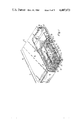
- FIG. 1 is a perspective view, partially broken away, of a flat panel display device incorporating a preferred embodiment of a line cathode.
- FIG. 2 shows portions of a preferred embodiment of a line cathode made in accordance with the present inventive method.
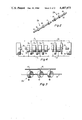
- FIG. 3 shows, in simplified form, an apparatus for carrying out one method of producing the line cathode of FIG. 2.
- FIG. 4 shows, in simplified form, another apparatus suitable for carrying out another method of producing the line cathode of FIG. 2.
- FIG. 1 shows a flat panel display device 10 incorporating a line cathode of the type shown in FIG. 2.
- the display device 10 includes an evacuated envelope 11 having a display section 13 and an electron gun section 14.
- the envelope 11 includes a frontwall 16 and a baseplate 17 held in a spaced parallel relationship by sidewalls 18.
- a display screen 12 is positioned along the frontwall 16 and gives a visual output when struck by electrons.
- a plurality of spaced parallel support vanes 19 are arranged between the frontwalls 16 and the baseplate 17.
- the support vanes 19 provide the desired internal support against external atmospheric pressure and divide the envelope 11 into a plurality of channels 21.
- Each of the channels 21 encloses a pair of spaced parallel beam guide meshes 22 and 23 extending transversely, or horizontally, across the channels and longitudinally, or vertically, along the channels from the gun section 14 to the opposite sidewall 18.
- a cathode 26 is arranged to emit electrons into the spaces 24 between the guide mesh pairs.
- the guides meshes 22 and 23 include apertures 27 which are arranged in columns longitudinally along the channels 21 and in rows transversely across the channels.
- a focus mesh 28 is spaced above the upper guide mesh 22 in a parallel relationship therewith.
- a plurality of extraction electrodes 29 are arranged along the baseplate 17 to extend transversely across the channels 21 the full width of the display device 10.
- the extraction electrodes 29 are arranged directly beneath the rows of apertures 27 in the guide meshes 22 and 23.
- Appropriate biasing voltages are applied to the focus mesh 28 and the extraction electrodes 29 to cause the electrons emitted from the cathode 26 to be periodically focused between the guide meshes 22 and 23 and to propagate in the spaces 24 for the full length of the channels.
- An acceleration mesh 31 is arranged in a spaced parallel relation with the focus mesh 28 and contains a plurality of apertures 32 which also are aligned in columns longitudinally of the channels and in rows transversely of the channels.
- Scanning electrodes 33 are arranged on both sides of the support vanes 29 so that each vane supports a scanning electrode for two adjacent channels. Insulative beads 34 engage the meshes 22, 23, 28 and 31 to retain the meshes in the desired spaced relationship.
- the electron beams propagate in the spaces 24 between the guide meshes 22 and 23 until the production of one horizontal line of the visual display requires the beams to be directed toward the screen 12.
- Extraction of the electron beams from the spaces between the guide meshes is effected by applying a negative voltage to one of the extraction electrodes 29.
- the negative voltage causes the electron beams to pass through the apertures 27 in the guide meshes and the apertures 32 in the acceleration mesh 31 and the focus mesh 28.
- the extracted electron beams are horizontally scanned across the channels 21 by the application of varying voltages, such as sawtooth waveforms, to the scanning electrodes 33 on the sides of the support vanes 19.
- Every channel therefore, is horizontally scanned between the two support vanes 19 so that each channel contributes a portion of each horizontal line of the visual display on the faceplate 16.
- the same line cathode supplies the electrons for every channel and each channel contributes to every horizontal line of the display.
- the line cathode 26 of FIG. 1 can be of the type disclosed in U.S. Pat. No. 4,100,449; however, the use of a cathode of this type results in several disadvantages. Firstly, electron emission is desired only in the areas of the cathode which are aligned with the columns of apertures 32 in the guide meshes 22 and 23. Each of the columns of apertures serves as an electron beam guide so that three beams, one for each of the primary colors in a color display, propagate in each of the channels 24. For this reason, no emission is needed, or desired, between the columns of apertures or between the larger spaces which span adjacent channels.
- 4,199,705 is useful in preventing electron emission between the columns of apertures and between adjacent channels. However, it is nevertheless preferable to eliminate the emission of electrons in all areas where such emission is not required.
- large volumnes of gases are driven off. These gases must be evacuated from the envelope by use of a vacuum pump.
- the presence of emissive material in the areas where electron emission is not needed merely adds to the difficulty of evacuating these gases from the envelope. Additionally, larger amounts of gettering are required by the presence of the emissive material and the gettering, therefore, may not be sufficient to handle the sudden on-rush of gas.
- FIG. 2 shows two portions 37a and 37b of a line cathode in accordance with the present invention.
- the flat panel device shown in FIG. 1 will include 40 channels each of which is one inch (2.54 cm) wide and 30 inches (100 cm) long. Accordingly, the total length of the cathode must exceed 40 inches to provide sufficient length for mounting brackets and tensioning devices.
- FIG. 2 shows two of the portions 37a and 37b of the line cathode which are aligned with the channels 24.
- the cathode includes a heater filament 38, which typically is made of tungsten and has a diameter of about 10 mils (approximately 25 microns).
- the portion 37a includes three areas 39, 40 and 41 where electron emissive material is uniformly deposited about the filament 38.
- the emissive areas are spaced to align with the columns of apertures in the guide meshes 22 and 23 of FIG. 1.
- the second portion 37b is similarly constructed to include emissive areas 42, 43 and 44 which also are spaced to align with the columns of apertures in one of the channels 24.
- the spacing between the emissive areas 41 and 42 of the portions 37a and 37b respectively is selected to span the space between adjacent channels.
- Each of the emissive areas 39 through 44 has a dimension along the length of the filament 38 which is determined by the transverse dimension of the apertures in the beam guides. As presently contemplated, this is in the order of 80 mils (200 microns).
- the spacing between adjacent emissive areas in each channel is in the order approximately 120 mils (300 microns).
- the spacing between the emissive areas 41 and 42 of the adjacent channels is in the order of 500 mils (1.27 cm).
- FIG. 3 shows, in simplified form, an apparatus for carrying out a method of producing a cathode having localized emissive areas of the type shown in FIG. 2.
- the tungsten filament 38 is arranged concentric with conductive cylinders 46, 47 and 48 which are spaced in accordance with the spacing of the emissive areas 39, 40 and 41 of FIG. 2. Similar conductive cylinders also would be provided for all emissive areas along the entire length of the cathode.
- An electrode lead 49 is electrically connected to the cylinders 46, 47 and 48 so that a positive voltage V can be simultaneously applied to all the cylinders.
- the filament 38 also is connected to a voltage which is selected so that the voltage V applied to the input line 49 is more positive than that applied to the filament.
- the voltage difference between the filament 38 and the cylinders 46 through 48 is dependent upon the diameter of the cylinders and the filament as well as the rate at which the emissive coating is to be applied, and the desired thickness of the coating.
- the thickness of emissive coating is a function of the duration and magnitude of the applied voltage. As an example, using a diameter of 1.25 inch for the cylinders 46 through 48, setting the line 49 at +145 volts and filament 38 at ground results in a one mil (2.5 micron) coating in approximately 7 seconds. A decrease in the diameter of the cylinders permits a proportional decrease in the voltage differential.
- the diameter of the cylinders 46 through 48 is held as small as physical strength and handling considerations permit in order to improve the transition of the emissive coating to the filament.
- Both of the above voltage/diameter relationships result in a field gradient of approximately 50 volts/centimeter, which is in the typical range of cataphoretic deposition applications. Field gradients from about 20 volt/cm to about 100 volt/cm are typical.
- a number of cylinders equal to the number of emissive areas to be deposited are aligned and supported in a fixture.
- the details of the fixture are within the purview of one skilled in the art.
- the filament is tensioned to eliminate sag and is centered in the cylinders.
- the cylinders are electrically connected to a voltage source by the lead 49 so that all the cylinders can be simultaneously biased to the same voltage.
- the filament 38 is connected to ground or other desired potential at the same time the the cylinders are biased.
- the cylinders and filament are then emerged in a solution of electron emissive material of a type known in the art.
- the solution can be carbonate comprising about 13% CaCO 3 , 31% SrCO 3 and 56% BaCO 3 .
- the voltages are simultaneously applied to the cylinders and the filament for the time required to deposit the emissive material to the desired thickness.
- the carbonate material is conductive, but highly resistive so that current flows through the material during deposition. This current can be monitored as a means of observing the thickness of material deposited on the filament 38.
- the emissive material is deposited on the filament 38 in the areas where field gradients are created between the filament and the cylinders, deposition is minimized in the portions of the cathode which are between the cylinders.
- FIG. 4 shows a structure, in simplified form, for further minimizing the deposition of emissive material in the areas where electron emission is not desired.
- the tungsten filament 38 which is shown in several sections, is tensioned between two insulative supports 51 and 52.
- a physically rigid electrically conductive bus bar 53 spans the insulative supports 51 and 52 along the full length of the filament 38.
- a plurality of cylinders, such as 56, 57 and 58 equal in number to the number of emissive areas desired and arranged at the areas where the deposition of material is desired, are electrically connected to the bus bar 53.
- Another physically rigid conductive bus bar 54 extends between the insulative supports 51 and 52 and is electrically connected to a plurality of cylinders, such as 59, 61, 62 and 63 which are arranged at the areas where deposition of the electron emissive material is to be minimized. All the cylinders 56 through 63 are centered about the tungsten filament 38.
- the bus 54, the filament 38, and the bus 53, respectively, are biased at the voltages V 1 , V 2 , and V 3 , where V 3 >V.sub. 2 >V 1 .
- the diameter of the cylinders 56 through 58 can be in the order of about 0.25 inches (0.63 cm), and the diameter of the cylinder 59 through 63 can be in the order of about 125 inches (0.31 cm).
- the width (dimension along the filament) of the cylinders 56 through 58 is equal to the desired width of the emissive areas 39 to 44 of FIG. 2.
- the width of the cylinders 61 and 62 is equal to the spacing between the emissive areas within one channel, such as between 39 and 40 or 43 and 44 of FIG. 2.
- the width of the cylinders 59 and 63, both of which are shown broken away, is equal to the spacing between the emissive areas of adjacent channels, such as the spacing between the areas 41 and 42 of FIG. 2.
- V 1 can be 0 volts, V 2 in the order of 50 volts, and V 3 in the order of 75 volts.
- V 2 is more positive than V 1 and current flows in a direction which prohibits deposition of the emissive material onto the electrode 38 portions within the cylinders biased at V 1
- the cylinders 56 to 58 are biased at the more positive V 3 than the filament 38 bias of V 2 , and the emissive material is deposited onto the filament portions inside the cylinders biased at the V 3 voltage.
- the entire apparatus is submerged in the emissive material with voltages V 1 , V 2 , and V 3 turned off.
- the voltages are simultaneously applied to all the cylinders.
- the duration of the application of the voltages is dependent upon the diameters of the cylinders and the thickness of the emissive material to be deposited onto the filament 38.
Landscapes
- Engineering & Computer Science (AREA)
- Manufacturing & Machinery (AREA)
- Cathode-Ray Tubes And Fluorescent Screens For Display (AREA)
Priority Applications (6)
| Application Number | Priority Date | Filing Date | Title |
|---|---|---|---|
| US06/370,582 US4487673A (en) | 1982-04-21 | 1982-04-21 | Method of making a line cathode having localized emissive coating |
| IT47793/83A IT1205332B (it) | 1982-04-21 | 1983-02-25 | Catodo lineare presentante un rivestimento emittente localizzato e metodo di fabbricazione dello stesso |
| GB08310406A GB2119564A (en) | 1982-04-21 | 1983-04-18 | Line cathode having localized emissive coating and method of making |
| JP58068250A JPS58192247A (ja) | 1982-04-21 | 1983-04-18 | 線状フイラメントの局部領域に電子放射材料を被着する方法 |
| DE19833314213 DE3314213A1 (de) | 1982-04-21 | 1983-04-20 | Linienkathode und verfahren zu ihrer herstellung |
| FR8306446A FR2525809A1 (fr) | 1982-04-21 | 1983-04-20 | Procede de fabrication d'une cathode pour dispositifs d'affichage electronique, et cathode ainsi obtenue |
Applications Claiming Priority (1)
| Application Number | Priority Date | Filing Date | Title |
|---|---|---|---|
| US06/370,582 US4487673A (en) | 1982-04-21 | 1982-04-21 | Method of making a line cathode having localized emissive coating |
Publications (1)
| Publication Number | Publication Date |
|---|---|
| US4487673A true US4487673A (en) | 1984-12-11 |
Family
ID=23460267
Family Applications (1)
| Application Number | Title | Priority Date | Filing Date |
|---|---|---|---|
| US06/370,582 Expired - Fee Related US4487673A (en) | 1982-04-21 | 1982-04-21 | Method of making a line cathode having localized emissive coating |
Country Status (6)
| Country | Link |
|---|---|
| US (1) | US4487673A (ja) |
| JP (1) | JPS58192247A (ja) |
| DE (1) | DE3314213A1 (ja) |
| FR (1) | FR2525809A1 (ja) |
| GB (1) | GB2119564A (ja) |
| IT (1) | IT1205332B (ja) |
Cited By (2)
| Publication number | Priority date | Publication date | Assignee | Title |
|---|---|---|---|---|
| US4806218A (en) * | 1986-09-05 | 1989-02-21 | Nokia Graetz Gmbh | Method of coating cathode wires by cataphoretic coating |
| WO1996035221A1 (en) * | 1995-05-02 | 1996-11-07 | Philips Electronics N.V. | Method and apparatus for depositing cathode material on a wire cathode |
Citations (8)
| Publication number | Priority date | Publication date | Assignee | Title |
|---|---|---|---|---|
| GB1014200A (en) * | 1961-09-05 | 1965-12-22 | Heraeus Gmbh W C | Improvements in or relating to electron beam guns |
| GB1025168A (en) * | 1963-09-20 | 1966-04-06 | Philips Electronic Associated | Improvements relating to cathode assemblies for electric discharge tubes |
| GB1290993A (ja) * | 1970-03-10 | 1972-09-27 | ||
| US4026780A (en) * | 1976-04-05 | 1977-05-31 | Rca Corporation | Method and apparatus for cataphoretic deposition |
| US4100449A (en) * | 1976-04-05 | 1978-07-11 | Rca Corporation | Uniform filament and method of making the same |
| GB2029632A (en) * | 1978-09-02 | 1980-03-19 | English Electric Valve Co Ltd | Magnetrons |
| US4199705A (en) * | 1978-12-04 | 1980-04-22 | Rca Corporation | Modulator structure for a flat panel display device |
| GB2070851A (en) * | 1980-02-29 | 1981-09-09 | Rca Corp | Unitary beam guide/electron gun assembly for flat panel display devices |
-
1982
- 1982-04-21 US US06/370,582 patent/US4487673A/en not_active Expired - Fee Related
-
1983
- 1983-02-25 IT IT47793/83A patent/IT1205332B/it active
- 1983-04-18 JP JP58068250A patent/JPS58192247A/ja active Pending
- 1983-04-18 GB GB08310406A patent/GB2119564A/en not_active Withdrawn
- 1983-04-20 FR FR8306446A patent/FR2525809A1/fr not_active Withdrawn
- 1983-04-20 DE DE19833314213 patent/DE3314213A1/de not_active Withdrawn
Patent Citations (9)
| Publication number | Priority date | Publication date | Assignee | Title |
|---|---|---|---|---|
| GB1014200A (en) * | 1961-09-05 | 1965-12-22 | Heraeus Gmbh W C | Improvements in or relating to electron beam guns |
| GB1025168A (en) * | 1963-09-20 | 1966-04-06 | Philips Electronic Associated | Improvements relating to cathode assemblies for electric discharge tubes |
| GB1290993A (ja) * | 1970-03-10 | 1972-09-27 | ||
| US4026780A (en) * | 1976-04-05 | 1977-05-31 | Rca Corporation | Method and apparatus for cataphoretic deposition |
| US4100449A (en) * | 1976-04-05 | 1978-07-11 | Rca Corporation | Uniform filament and method of making the same |
| GB1575530A (en) * | 1976-04-05 | 1980-09-24 | Rca Corp | Filament and method of making same |
| GB2029632A (en) * | 1978-09-02 | 1980-03-19 | English Electric Valve Co Ltd | Magnetrons |
| US4199705A (en) * | 1978-12-04 | 1980-04-22 | Rca Corporation | Modulator structure for a flat panel display device |
| GB2070851A (en) * | 1980-02-29 | 1981-09-09 | Rca Corp | Unitary beam guide/electron gun assembly for flat panel display devices |
Cited By (5)
| Publication number | Priority date | Publication date | Assignee | Title |
|---|---|---|---|---|
| US4806218A (en) * | 1986-09-05 | 1989-02-21 | Nokia Graetz Gmbh | Method of coating cathode wires by cataphoretic coating |
| WO1996035221A1 (en) * | 1995-05-02 | 1996-11-07 | Philips Electronics N.V. | Method and apparatus for depositing cathode material on a wire cathode |
| US5714051A (en) * | 1995-05-02 | 1998-02-03 | U.S. Philips Corporation | Method for depositing cathode material on a wire cathode |
| US5902464A (en) * | 1995-05-02 | 1999-05-11 | U.S. Philips Corporation | Apparatus for depositing cathode material on a wire cathode |
| KR100395380B1 (ko) * | 1995-05-02 | 2003-12-01 | 코닌클리케 필립스 일렉트로닉스 엔.브이. | 와이어캐소드상에캐소드물질을침착하기위한장치및와이어캐소드제조방법 |
Also Published As
| Publication number | Publication date |
|---|---|
| GB2119564A (en) | 1983-11-16 |
| DE3314213A1 (de) | 1983-11-10 |
| FR2525809A1 (fr) | 1983-10-28 |
| IT1205332B (it) | 1989-03-15 |
| GB8310406D0 (en) | 1983-05-25 |
| IT8347793A0 (it) | 1983-02-25 |
| JPS58192247A (ja) | 1983-11-09 |
Similar Documents
| Publication | Publication Date | Title |
|---|---|---|
| JP3160213B2 (ja) | 強誘電性エミッターを適用した陰極構造体及びこれを適用した電子銃並びに陰極線管 | |
| US5859508A (en) | Electronic fluorescent display system with simplified multiple electrode structure and its processing | |
| US5729244A (en) | Field emission device with microchannel gain element | |
| US5055744A (en) | Display device | |
| JP2782224B2 (ja) | 画像形成装置の駆動方法 | |
| US4162427A (en) | Gas-discharge display panel | |
| US4487673A (en) | Method of making a line cathode having localized emissive coating | |
| US7233301B2 (en) | Flat panel display and method of manufacturing the same | |
| JPH11509013A (ja) | プラズマを含有するディスプレイデバイス用の中空状カソード及びこの中空状カソードの製造方法 | |
| US4881005A (en) | Flat type display device | |
| US4131823A (en) | Modular flat display device with beam convergence | |
| JP2759483B2 (ja) | 画像形成装置の駆動方法 | |
| US4970430A (en) | Fluorescent display apparatus | |
| JPH0349135A (ja) | 平板型表示装置 | |
| US4322657A (en) | Gas-discharge display device | |
| US6188178B1 (en) | Flat-panel picture display device with spacer means adjacent the display screen | |
| US7138761B2 (en) | Field emission display and driving method thereof | |
| JP2888589B2 (ja) | 画像表示装置 | |
| KR100522692B1 (ko) | 전계 방출 소자 및, 그것의 제조 방법 | |
| JPH1096902A (ja) | アドレス指定構体用陰極及びスパッタリング損傷軽減方法 | |
| US20050231088A1 (en) | Mesh structure of tetraode field-emission display and method of fabricating the same | |
| JP2789210B2 (ja) | 電子線発生装置及び該電子線発生装置を用いた画像形成装置 | |
| KR0166020B1 (ko) | 평판표시장치 | |
| JPS61171032A (ja) | 画像表示装置の製造方法 | |
| US20050231089A1 (en) | Mesh structure of tetraode field-emission display and method of fabricating the same |
Legal Events
| Date | Code | Title | Description |
|---|---|---|---|
| AS | Assignment |
Owner name: RCA CORPORATION, A CORP. OF DE. Free format text: ASSIGNMENT OF ASSIGNORS INTEREST.;ASSIGNOR:STEINMETZ, CARL C.;REEL/FRAME:004016/0340 Effective date: 19820420 Owner name: RCA CORPORATION, NEW JERSEY Free format text: ASSIGNMENT OF ASSIGNORS INTEREST;ASSIGNOR:STEINMETZ, CARL C.;REEL/FRAME:004016/0340 Effective date: 19820420 |
|
| CC | Certificate of correction | ||
| AS | Assignment |
Owner name: RCA LICENSING CORPORATION, TWO INDEPENDENCE WAY, P Free format text: ASSIGNMENT OF ASSIGNORS INTEREST.;ASSIGNOR:RCA CORPORATION, A CORP. OF DE;REEL/FRAME:004993/0131 Effective date: 19871208 |
|
| FPAY | Fee payment |
Year of fee payment: 4 |
|
| REMI | Maintenance fee reminder mailed | ||
| LAPS | Lapse for failure to pay maintenance fees | ||
| FP | Lapsed due to failure to pay maintenance fee |
Effective date: 19921213 |
|
| STCH | Information on status: patent discontinuation |
Free format text: PATENT EXPIRED DUE TO NONPAYMENT OF MAINTENANCE FEES UNDER 37 CFR 1.362 |