US4341593A - Plasma etching method for aluminum-based films - Google Patents
Plasma etching method for aluminum-based films Download PDFInfo
- Publication number
- US4341593A US4341593A US06/177,910 US17791080A US4341593A US 4341593 A US4341593 A US 4341593A US 17791080 A US17791080 A US 17791080A US 4341593 A US4341593 A US 4341593A
- Authority
- US
- United States
- Prior art keywords
- etching
- aluminum
- plasma
- cathode
- chlorine gas
- Prior art date
- Legal status (The legal status is an assumption and is not a legal conclusion. Google has not performed a legal analysis and makes no representation as to the accuracy of the status listed.)
- Expired - Lifetime
Links
Images


Classifications
-
- H—ELECTRICITY
- H01—ELECTRIC ELEMENTS
- H01L—SEMICONDUCTOR DEVICES NOT COVERED BY CLASS H10
- H01L21/00—Processes or apparatus adapted for the manufacture or treatment of semiconductor or solid state devices or of parts thereof
- H01L21/02—Manufacture or treatment of semiconductor devices or of parts thereof
- H01L21/04—Manufacture or treatment of semiconductor devices or of parts thereof the devices having potential barriers, e.g. a PN junction, depletion layer or carrier concentration layer
- H01L21/18—Manufacture or treatment of semiconductor devices or of parts thereof the devices having potential barriers, e.g. a PN junction, depletion layer or carrier concentration layer the devices having semiconductor bodies comprising elements of Group IV of the Periodic Table or AIIIBV compounds with or without impurities, e.g. doping materials
- H01L21/30—Treatment of semiconductor bodies using processes or apparatus not provided for in groups H01L21/20 - H01L21/26
- H01L21/31—Treatment of semiconductor bodies using processes or apparatus not provided for in groups H01L21/20 - H01L21/26 to form insulating layers thereon, e.g. for masking or by using photolithographic techniques; After treatment of these layers; Selection of materials for these layers
- H01L21/3205—Deposition of non-insulating-, e.g. conductive- or resistive-, layers on insulating layers; After-treatment of these layers
- H01L21/321—After treatment
- H01L21/3213—Physical or chemical etching of the layers, e.g. to produce a patterned layer from a pre-deposited extensive layer
- H01L21/32133—Physical or chemical etching of the layers, e.g. to produce a patterned layer from a pre-deposited extensive layer by chemical means only
- H01L21/32135—Physical or chemical etching of the layers, e.g. to produce a patterned layer from a pre-deposited extensive layer by chemical means only by vapour etching only
- H01L21/32136—Physical or chemical etching of the layers, e.g. to produce a patterned layer from a pre-deposited extensive layer by chemical means only by vapour etching only using plasmas
-
- C—CHEMISTRY; METALLURGY
- C23—COATING METALLIC MATERIAL; COATING MATERIAL WITH METALLIC MATERIAL; CHEMICAL SURFACE TREATMENT; DIFFUSION TREATMENT OF METALLIC MATERIAL; COATING BY VACUUM EVAPORATION, BY SPUTTERING, BY ION IMPLANTATION OR BY CHEMICAL VAPOUR DEPOSITION, IN GENERAL; INHIBITING CORROSION OF METALLIC MATERIAL OR INCRUSTATION IN GENERAL
- C23F—NON-MECHANICAL REMOVAL OF METALLIC MATERIAL FROM SURFACE; INHIBITING CORROSION OF METALLIC MATERIAL OR INCRUSTATION IN GENERAL; MULTI-STEP PROCESSES FOR SURFACE TREATMENT OF METALLIC MATERIAL INVOLVING AT LEAST ONE PROCESS PROVIDED FOR IN CLASS C23 AND AT LEAST ONE PROCESS COVERED BY SUBCLASS C21D OR C22F OR CLASS C25
- C23F4/00—Processes for removing metallic material from surfaces, not provided for in group C23F1/00 or C23F3/00
Definitions
- the present invention relates to a plasma etching method and more particularly to a plasma etching method for aluminum-based films.
- the plasma etching method using a fluorocarbon gas such as carbon tetrafluoride as a plasma generating gas is widely used for etching polycrystalline silicon films or silicon nitride films in the manufacture of LSIs.
- a fluorocarbon gas such as carbon tetrafluoride
- carbon tetrachloride is used as a plasma generating gas for etching aluminum films.
- the chlorine radicals or ions in the generated plasma react with aluminum to convert it to aluminum chloride.
- the aluminum chloride is then etched.
- the conventional plasma etching method further presents practical problems since etching selectivity for aluminum over silicon or silicon oxide is relatively low. For example, when the thickness of an aluminum film formed on a silicon substrate or a silicon oxide film is not uniform, etching at thinner portions is completed before etching at thicker portions is completed. Thus, the silicon substrate or the silicon oxide film below these thinner portions is etched while the rest of the thicker portions are being etched. This might well lead to damage of elements.
- etching tends to progress into portions of the aluminum film covered by a resist mask of a predetermined pattern (lateral etching) and the resist mask sometimes swells during aluminum etching. This presents problems in fine processing.
- an object of the present invention to provide a plasma etching method in which there is no time lag before initiating etching of aluminum-based films and by which aluminum-based films may be selectively etched with precision.
- the present invention provides a plasma etching method which comprises the steps of:
- a plasma generating gas consisting of carbon tetrachloride and chlorine gas at a pressure of 0.1 Torr or less between said anode and cathode, the ratio of the partial pressure of said chlorine gas to the total pressure being 0.8 or less;
- the aluminum-based film covers the silicon substrate or the silicon oxide film.
- the ratio of the partial pressure of the chlorine gas to the total pressure is generally 0.1 or more, preferably 0.2 or more and more preferably 0.6 or more.
- the plasma generating gas is preferably charged to a pressure of 0.01-0.06 Torr, and more preferably 0.02-0.06 Torr.
- the aluminum-based film is covered with a resist film of a predetermined pattern.
- the ratio of the partial pressure of the chlorine gas to the total pressure is generally 0.6 or less, preferably 0.2-0.45, and more preferably 0.3-0.35.
- the etching is performed at a cathode fall voltage of -50 V or less and preferably -50 V to -220 V.
- FIG. 1 is a schematic view of an apparatus to be used in the plasma etching method of the present invention
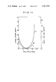
- FIG. 2 is a graph showing the etching speed of an aluminum film by the plasma generating gas used in the present invention in comparison with that by conventional carbon tetrachloride;
- FIG. 3 is a graph showing the relation between the ratio of the partial pressure of the chlorine gas of the plasma generating gas used in the present invention and the cathode fall voltage;
- FIG. 4 is a graph showing the change of cathode fall voltage in relation to the change in total pressure of the plasma generating gas of the present invention
- FIG. 5 is a view for explicating the cathode fall voltage
- FIGS. 6A-6C are sectional views illustrating the state of a workpiece etched according to the present invention.
- FIGS. 7 and 8 are graphs showing the etching characteristics of the plasma generating gas used in the present invention under different constant pressures, respectively;
- FIG. 9 is a graph showing the etching characteristics of the plasma generating gas used in the present invention under different pressures.
- FIG. 10 is a graph showing the relation between the lateral etching amount of the aluminum film and the resist swelling amount, and the total pressure of the plasma generating gas used in the present invention.
- FIG. 11 is a graph showing the relation between the ratio of the lateral etching amount of the aluminum film and the resist swelling amount, and the partial pressure of the chlorine gas of the plasma generating gas used in the present invention.
- FIG. 1 shows an apparatus used in the plasma etching method of the present invention.
- the plasma etching apparatus includes a sealed container 1 of, for example, a stainless steel which has an inlet port 2 for carbon tetrachloride and an inlet port 3 for chlorine gas.
- a plate anode 4 constituting part of the wall thereof and a plate cathode 5 arranged parallel to the anode.
- a plasma etching chamber 6 is formed between these electrodes 4 and 5.
- the anode 4 is insulated from the container 1 by insulating bodies 8 and 9 of, for example, Teflon and is grounded through a lead wire 10.
- the cathode 5 is supported through insulating bodies 11 and 12 by a support plate 7 arranged in the container so as to form a space 13 between the cathode and itself.
- the cathode is connected through the space 13, the airtight part 27, the lead wire 14 and an external matching circuit 15 to a high frequency power source 16.
- Water cooling pipes 19 and 20 for removing the heat generated during etching are disposed at the respective electrodes 4 and 5.
- the container 1 further has a relatively large outlet port 21 for the plasma generating gas where two conductance valves 22 and 24 for controlling the internal pressure of the container 1 are disposed through a liquid nitrogen trap 23.
- the conductance valve 24 at the lower stream is connected to an exhausting means such as a diffusion pump, a Roots pump or a rotary pump.
- a high frequency voltage detecting probe 17 is interposed between the cathode 5 and the matching circuit 15. This probe 17 drops the detecting voltage to 1/1,000 its original value and supplies it to a synchroscope 18. The inside of the etching chamber 6 can be observed through an observation window 25.
- a workpiece 26 having an aluminum-based film with an exposed portion for example, an aluminum-based film which is formed on a silicon substrate or on a silicon oxide film formed on a silicon substrate and which is covered with a resist mask with a predetermined pattern is placed on the cathode.
- an aluminum-based film films of aluminum with several % of silicon or copper mixed therewith may also be used in place of films of pure aluminum.
- the carbon tetrachloride and the chlorine gases are charged into the container 1 through inlets 2 and 3, respectively.
- the internal pressure of the container 1 is adjusted by the conductance valves 22 and 24.
- a high frequency electric power is applied from a power source 16 (generally from 100 W (0.12 W/cm 2 ) to 300 W (0.36 W/cm 2 )) to the electrodes 4 and 5 while cooling these electrodes 4 and 5 by the cooling pipes 19 and 20. Then a glow discharge is effected, and a plasma is generated between both electrodes. The exposed portion of the aluminum-based film of the workpiece 26 is etched by this plasma.
- the present invention is principally based on the finding that the time lag in the initiation of the etching of the aluminum film is significantly reduced when chlorine gas is added to carbon tetrachloride which has been conventionally used as the plasma generating gas. That is, the present inventors etched the aluminum films using carbon tetrachloride and a mixture of carbon tetrachloride and chlorine gas and measured the etching speed in each case. The results obtained are shown in FIG. 2. In the figure, the line a shows a case when etching was performed using the carbon tetrachloride alone under the conditions of 200 W in RF electric power and 0.04 Torr in pressure.
- Lines b, c, d and e show the cases when a mixture of carbon tetrachloride and chlorine gas was charged such that the ratio of the partial pressure of the chlorine gas to the total pressure was 15/40 (PCl 2 /PCl 2 +PCCl 4 ) and the etching was performed under the pressure of 0.1 Torr, 0.08 Torr, 0.06 Torr and 0.04 Torr, respectively by adjusting the pressure with a main valve 22.
- the time required before the initiation of the etching is far shorter with a mixture of the carbon tetrachloride gas and chlorine gas than with carbon tetrachloride gas alone as the plasma generating gas. This effect is even more pronounced when the pressure during the etching is reduced.
- the present inventors studied improvements in the etching selectivity for aluminum-based metals over silicon and silicon dioxide. As a result, it was found that when the ratio of the partial pressure of the chlorine gas to the total pressure (PCl 2 /(PCCl 4 +PCl 2 )) is 0.8 or less and the total pressure during etching is 0.1 Torr or less, the etching selectivity for aluminum-based metals over silicon and silicon dioxide was improved.
- the ratio of the partial pressure of the chlorine gas to the total pressure is preferably 0.01 or more especially 0.2 or more, more preferably 0.4-0.8, and most preferably 0.6-0.8 for the purpose of improved selectivity.
- the ratio of the partial pressure of the chlorine gas to the total pressure is 0.7 or less, and more preferably 0.6 or less, stable etching may be performed since the etching speed and the selectivity of the aluminum-based metals do not change abruptly.
- the etching selectivity for aluminum-based metals is extremely good when the pressure during etching is 0.01 Torr or more, and more preferably 0.02-0.06 Torr.
- the applied electric power does not provide much influence on the etching selectivity for aluminum-based metals, and similar results are obtained in the range of 100 W (0.12 W/cm 2 ) to 300 W (0.36 W/cm 2 ).
- the etching pressure was found to be closely related to the cathode fall voltage (Vdc).
- Vdc cathode fall voltage
- the relation between the partial pressure of the chlorine gas to the total pressure and Vdc was substantially constant as shown by the curves a, b and c in FIG. 3 when the etching pressure was constant and the RF electric power was 100 W (0.12 W/cm 2 ), 200 W (0.24 W/cm 2 ) and 300 W (0.36 W/cm 2 ).
- Vdc the cathode fall voltage
- the cathode fall voltage (Vdc) is generated by the drop in the potential at the cathode for attaining equilibrium when the electrons in the plasma flow at the positive half period and the positive ions flow at the negative half period to the cathode, which may otherwise be disturbed by the greater transfer force of the electrons.
- the cathode fall voltage may be correctly represented as (V 1 +V 2 )/2 as shown in FIG. 5, but is generally represented as V 2 /2 since V 1 is small enough.
- the present inventors have further studied the lateral etching and the swelling and deformation of the resist film in the etching of an aluminum-based film below a resist film using a plasma generating gas consisting of carbon tetrachloride gas and chlorine gas. It was learned that Vdc as well as the ratio of the chlorine gas partial pressure to the total pressure are closely related to these problems. When etching was performed at a ratio of the chlorine gas partial pressure to the total pressure of 0.6 or less and a cathode fall voltage of -20 V or less, the lateral etching was substantially decreased.
- the ratio of the chlorine gas partial pressure to the total pressure is preferably 0.2-0.45 and more preferably 0.3-0.35, and the cathode fall voltage is preferably -50 V to -220 V.
- a residue 64 (this mainly consisted of Al according to an electron probe microanalysis) is deposited on the side faces of the resist film 63 and of the aluminum-based film 62 therebelow as shown in FIG. 6A. The lateral etching of the aluminum-based film is prevented by the existence of this residue 64.
- the resist film 63 is etched by an oxygen plasma (FIG.
- the etching is preferably performed under the condition that the ratio of the chlorine gas partial pressure to the total pressure is 0.2-0.6, the etching pressure is 0.1 Torr or less, and the cathode fall voltage is -50 V to -220 V.
- the etching pressure was kept constant at 0.1 and 0.04 Torr and the ratio of the chlorine gas partial pressure to the total pressure was varied.
- the etching speeds of the aluminum film, and silicon substrate, and the silicon oxide film were measured. The results are shown in FIG. 7 (0.1 Torr), and in FIG. 8 (0.04 Torr).
- curve a shows the case of the aluminum film
- curve b shows the case of the silicon substrate
- curve c shows the case of the silicon dioxide film.
- Curves d and e show the etching selectivity for aluminum over silicon and for aluminum over silicon oxide.
- the chlorine gas partial pressure ratio was kept constant at 0.015/0.04 and the etching pressure was changed (0.04, 0.05, 0.07, 0.085, 0.1, 0.11 and 0.12 Torr).
- the etching speeds of the aluminum film, the silicon substrate, and the silicon oxide film were measured. The results are shown in FIG. 9.
- curve a shows the case for the aluminum film
- curve b shows the case for the silicon substrate
- curve c shows the case for the silicon oxide film.
- the curves d and e are the etching selectivities for Al/Si and Al/SiO 2 .
- the chlorine gas partial pressure ratio was kept constant at 0.015/0.04, a high frequency electric power of 200 W was used, and the etching pressure was charged for etching the aluminum film below the resist mask.
- the lateral etching of the aluminum film and the resist swelling were measured. The results are shown in FIG. 10.
- curve a shows the lateral etching
- curve b shows the resist swelling. Lateral etching exceeding the thickness of the aluminum film was observed in the aluminum film when the etching pressure was more than 0.1 Torr.
- the cathode voltage drop is preferably -20 V or less.
- the etching pressure was kept constant at 0.04 Torr, a high frequency electric power of 200 W was used, and the chlorine gas partial pressure ratio was changed.
- the lateral etching of the aluminum film below the resist film and the swelling of the resist were measured. The results are shown in FIG. 11. In this figure, curve a shows the lateral etching of the aluminum film and curve b shows the resist swelling.
Landscapes
- Engineering & Computer Science (AREA)
- Chemical & Material Sciences (AREA)
- Physics & Mathematics (AREA)
- Chemical Kinetics & Catalysis (AREA)
- Condensed Matter Physics & Semiconductors (AREA)
- Organic Chemistry (AREA)
- Mechanical Engineering (AREA)
- Plasma & Fusion (AREA)
- Materials Engineering (AREA)
- General Chemical & Material Sciences (AREA)
- Metallurgy (AREA)
- General Physics & Mathematics (AREA)
- Manufacturing & Machinery (AREA)
- Computer Hardware Design (AREA)
- Microelectronics & Electronic Packaging (AREA)
- Power Engineering (AREA)
- Drying Of Semiconductors (AREA)
- ing And Chemical Polishing (AREA)
Applications Claiming Priority (6)
| Application Number | Priority Date | Filing Date | Title |
|---|---|---|---|
| JP54/104032 | 1979-08-17 | ||
| JP10403279A JPS5629328A (en) | 1979-08-17 | 1979-08-17 | Plasma etching method |
| JP12420979A JPS5647570A (en) | 1979-09-28 | 1979-09-28 | Plasma etching method |
| JP54/124209 | 1979-09-28 | ||
| JP12420779A JPS6056231B2 (ja) | 1979-09-28 | 1979-09-28 | プラズマエッチング方法 |
| JP54/124207 | 1979-09-28 |
Publications (1)
| Publication Number | Publication Date |
|---|---|
| US4341593A true US4341593A (en) | 1982-07-27 |
Family
ID=27310132
Family Applications (1)
| Application Number | Title | Priority Date | Filing Date |
|---|---|---|---|
| US06/177,910 Expired - Lifetime US4341593A (en) | 1979-08-17 | 1980-08-14 | Plasma etching method for aluminum-based films |
Country Status (4)
| Country | Link |
|---|---|
| US (1) | US4341593A (OSRAM) |
| DE (1) | DE3030814C2 (OSRAM) |
| FR (1) | FR2463976A1 (OSRAM) |
| GB (1) | GB2059879B (OSRAM) |
Cited By (8)
| Publication number | Priority date | Publication date | Assignee | Title |
|---|---|---|---|---|
| US4436584A (en) | 1983-03-21 | 1984-03-13 | Sperry Corporation | Anisotropic plasma etching of semiconductors |
| US4838992A (en) * | 1987-05-27 | 1989-06-13 | Northern Telecom Limited | Method of etching aluminum alloys in semi-conductor wafers |
| US5106471A (en) * | 1990-04-02 | 1992-04-21 | Motorola, Inc. | Reactive ion etch process for surface acoustic wave (SAW) device fabrication |
| US5198072A (en) * | 1990-07-06 | 1993-03-30 | Vlsi Technology, Inc. | Method and apparatus for detecting imminent end-point when etching dielectric layers in a plasma etch system |
| US20060081846A1 (en) * | 2000-02-22 | 2006-04-20 | Semiconductor Energy Laboratory Co., Ltd. | Semiconductor device and method of manufacturing the same |
| US20100062607A1 (en) * | 2008-09-11 | 2010-03-11 | Tokyo Electron Limited | Dry etching method |
| EP2484382A1 (en) | 2005-03-30 | 2012-08-08 | Schering Corporation | Medicament comprising a phosphodiesterase IV inhibitor in an inhalable form |
| US8487315B2 (en) | 2000-04-12 | 2013-07-16 | Semiconductor Energy Laboratory Co., Ltd. | Illumination apparatus |
Families Citing this family (2)
| Publication number | Priority date | Publication date | Assignee | Title |
|---|---|---|---|---|
| DE3272669D1 (en) * | 1982-03-18 | 1986-09-25 | Ibm Deutschland | Plasma-reactor and its use in etching and coating substrates |
| JPH04125924A (ja) * | 1990-09-17 | 1992-04-27 | Mitsubishi Electric Corp | プラズマエッチング方法 |
Citations (2)
| Publication number | Priority date | Publication date | Assignee | Title |
|---|---|---|---|---|
| US3994793A (en) * | 1975-05-22 | 1976-11-30 | International Business Machines Corporation | Reactive ion etching of aluminum |
| US4182646A (en) * | 1978-07-27 | 1980-01-08 | John Zajac | Process of etching with plasma etch gas |
Family Cites Families (2)
| Publication number | Priority date | Publication date | Assignee | Title |
|---|---|---|---|---|
| FR2312114A1 (fr) * | 1975-05-22 | 1976-12-17 | Ibm | Attaque de materiaux par ions reactifs |
| CA1059882A (en) * | 1976-08-16 | 1979-08-07 | Northern Telecom Limited | Gaseous plasma etching of aluminum and aluminum oxide |
-
1980
- 1980-08-14 US US06/177,910 patent/US4341593A/en not_active Expired - Lifetime
- 1980-08-14 DE DE3030814A patent/DE3030814C2/de not_active Expired
- 1980-08-18 FR FR8018069A patent/FR2463976A1/fr active Granted
- 1980-08-18 GB GB8026885A patent/GB2059879B/en not_active Expired
Patent Citations (2)
| Publication number | Priority date | Publication date | Assignee | Title |
|---|---|---|---|---|
| US3994793A (en) * | 1975-05-22 | 1976-11-30 | International Business Machines Corporation | Reactive ion etching of aluminum |
| US4182646A (en) * | 1978-07-27 | 1980-01-08 | John Zajac | Process of etching with plasma etch gas |
Non-Patent Citations (2)
| Title |
|---|
| Preprint for 26th Applied Physics Meeting, 311 (1979) by K. Ueki et al. (Hitachi Ltd.). * |
| Semiconductor Integrated Circuit Symposium . . . 15th Lecture Articles (Electrochemical Association), 60 (1979) by H. Kinoshita et al Toshiba (NTIS), pp. 60-65. * |
Cited By (18)
| Publication number | Priority date | Publication date | Assignee | Title |
|---|---|---|---|---|
| US4436584A (en) | 1983-03-21 | 1984-03-13 | Sperry Corporation | Anisotropic plasma etching of semiconductors |
| US4838992A (en) * | 1987-05-27 | 1989-06-13 | Northern Telecom Limited | Method of etching aluminum alloys in semi-conductor wafers |
| US5106471A (en) * | 1990-04-02 | 1992-04-21 | Motorola, Inc. | Reactive ion etch process for surface acoustic wave (SAW) device fabrication |
| US5198072A (en) * | 1990-07-06 | 1993-03-30 | Vlsi Technology, Inc. | Method and apparatus for detecting imminent end-point when etching dielectric layers in a plasma etch system |
| US20110169011A1 (en) * | 2000-02-22 | 2011-07-14 | Semiconductor Energy Laboratory Co., Ltd. | Semiconductor device and method of manufacturing the same |
| US8399884B2 (en) | 2000-02-22 | 2013-03-19 | Semiconductor Energy Laboratory Co., Ltd. | Semiconductor device and method of manufacturing the same |
| US9869907B2 (en) | 2000-02-22 | 2018-01-16 | Semiconductor Energy Laboratory Co., Ltd. | Semiconductor device and method of manufacturing the same |
| US7915615B2 (en) | 2000-02-22 | 2011-03-29 | Semiconductor Energy Laboratory Co., Ltd. | Semiconductor device and method of manufacturing the same |
| US20060081846A1 (en) * | 2000-02-22 | 2006-04-20 | Semiconductor Energy Laboratory Co., Ltd. | Semiconductor device and method of manufacturing the same |
| US9318610B2 (en) | 2000-02-22 | 2016-04-19 | Semiconductor Energy Laboratory Co., Ltd. | Semiconductor device and method of manufacturing the same |
| US8704233B2 (en) | 2000-02-22 | 2014-04-22 | Semiconductor Energy Laboratory Co., Ltd. | Semiconductor device and method of manufacturing the same |
| US7566903B2 (en) | 2000-02-22 | 2009-07-28 | Semiconductor Energy Laboratory Co., Ltd. | Semiconductor device and method of manufacturing the same |
| US8487315B2 (en) | 2000-04-12 | 2013-07-16 | Semiconductor Energy Laboratory Co., Ltd. | Illumination apparatus |
| US8829529B2 (en) | 2000-04-12 | 2014-09-09 | Semiconductor Energy Laboratory Co., Ltd. | Illumination apparatus |
| US9704996B2 (en) | 2000-04-12 | 2017-07-11 | Semiconductor Energy Laboratory Co., Ltd. | Semiconductor device |
| EP2484382A1 (en) | 2005-03-30 | 2012-08-08 | Schering Corporation | Medicament comprising a phosphodiesterase IV inhibitor in an inhalable form |
| US8293655B2 (en) * | 2008-09-11 | 2012-10-23 | Tokyo Electron Limited | Dry etching method |
| US20100062607A1 (en) * | 2008-09-11 | 2010-03-11 | Tokyo Electron Limited | Dry etching method |
Also Published As
| Publication number | Publication date |
|---|---|
| DE3030814A1 (de) | 1981-02-26 |
| GB2059879B (en) | 1983-05-05 |
| FR2463976A1 (fr) | 1981-02-27 |
| GB2059879A (en) | 1981-04-29 |
| DE3030814C2 (de) | 1983-06-16 |
| FR2463976B1 (OSRAM) | 1984-09-21 |
Similar Documents
| Publication | Publication Date | Title |
|---|---|---|
| TWI725072B (zh) | 蝕刻方法 | |
| US5015331A (en) | Method of plasma etching with parallel plate reactor having a grid | |
| US4473436A (en) | Method of producing structures from double layers of metal silicide and polysilicon on integrated circuit substrates by RIE utilizing SF6 and Cl2 | |
| US5728278A (en) | Plasma processing apparatus | |
| JPH05308062A (ja) | ドライエッチング方法 | |
| JPS6352118B2 (OSRAM) | ||
| JPS627268B2 (OSRAM) | ||
| US4341593A (en) | Plasma etching method for aluminum-based films | |
| US4478678A (en) | Method of reactive ion etching molybdenum and molybdenum silicide | |
| US10950458B2 (en) | Etching method | |
| JPS6214429A (ja) | 表面処理方法及び表面処理装置 | |
| US20250149342A1 (en) | Etching method and plasma processing apparatus | |
| JPH0359573B2 (OSRAM) | ||
| US4566941A (en) | Reactive ion etching method | |
| US4554047A (en) | Downstream apparatus and technique | |
| Ephrath | The effect of cathode materials on reactive ion etching of silicon and silicon dioxide in a CF4 plasma | |
| US5110410A (en) | Zinc sulfide planarization | |
| US7883631B2 (en) | Plasma etching method, plasma etching apparatus, control program and computer-readable storage medium | |
| JPH0251987B2 (OSRAM) | ||
| US20030121888A1 (en) | Etching method | |
| JPH0121230B2 (OSRAM) | ||
| JPH0845858A (ja) | プラズマ処理装置 | |
| JP2768689B2 (ja) | ドライエッチング方法 | |
| JPH07263427A (ja) | プラズマエッチング方法 | |
| Tsukada | Characteristics of etch rate uniformity in aluminum reactive ion etching |
Legal Events
| Date | Code | Title | Description |
|---|---|---|---|
| AS | Assignment |
Owner name: TOKUDA SEISAKUSYO, LTD.; 1044-1, SAGAMIDAI, ZAMA- Free format text: ASSIGNMENT OF ASSIGNORS INTEREST.;ASSIGNORS:KURISAKI, TETUO;HORIIKE, YASUHIRO;YAMAZAKI, TAKASHI;REEL/FRAME:003988/0016 Effective date: 19800716 Owner name: TOKYO SHIBAURA DENKI KABUSHIKI KAISHA; 72 HORIKAWA Free format text: ASSIGNMENT OF ASSIGNORS INTEREST.;ASSIGNORS:KURISAKI, TETUO;HORIIKE, YASUHIRO;YAMAZAKI, TAKASHI;REEL/FRAME:003988/0016 Effective date: 19800716 |
|
| STCF | Information on status: patent grant |
Free format text: PATENTED CASE |
|
| AS | Assignment |
Owner name: SHIBAURA ENGINEERING WORKS CO., LTD., JAPAN Free format text: MERGER;ASSIGNOR:TOKUDA SEISAKUSHO CO., LTD.;REEL/FRAME:006375/0737 Effective date: 19911220 |