US4321663A - Process of pulse duration modulation of a multi-phase converter - Google Patents
Process of pulse duration modulation of a multi-phase converter Download PDFInfo
- Publication number
- US4321663A US4321663A US06/041,343 US4134379A US4321663A US 4321663 A US4321663 A US 4321663A US 4134379 A US4134379 A US 4134379A US 4321663 A US4321663 A US 4321663A
- Authority
- US
- United States
- Prior art keywords
- voltage
- time dependent
- phase
- load
- voltages
- Prior art date
- Legal status (The legal status is an assumption and is not a legal conclusion. Google has not performed a legal analysis and makes no representation as to the accuracy of the status listed.)
- Expired - Lifetime
Links
- 238000000034 method Methods 0.000 title claims abstract description 24
- 230000036962 time dependent Effects 0.000 claims abstract description 90
- 238000010586 diagram Methods 0.000 description 5
- 238000001228 spectrum Methods 0.000 description 4
- 239000000969 carrier Substances 0.000 description 2
- 230000007423 decrease Effects 0.000 description 2
- 230000001419 dependent effect Effects 0.000 description 2
- 230000000694 effects Effects 0.000 description 2
- 230000001965 increasing effect Effects 0.000 description 2
- 238000005070 sampling Methods 0.000 description 2
- 230000006399 behavior Effects 0.000 description 1
- 230000015572 biosynthetic process Effects 0.000 description 1
- 230000001939 inductive effect Effects 0.000 description 1
- 230000004048 modification Effects 0.000 description 1
- 238000012986 modification Methods 0.000 description 1
- 230000036961 partial effect Effects 0.000 description 1
Images


Classifications
-
- H—ELECTRICITY
- H02—GENERATION; CONVERSION OR DISTRIBUTION OF ELECTRIC POWER
- H02M—APPARATUS FOR CONVERSION BETWEEN AC AND AC, BETWEEN AC AND DC, OR BETWEEN DC AND DC, AND FOR USE WITH MAINS OR SIMILAR POWER SUPPLY SYSTEMS; CONVERSION OF DC OR AC INPUT POWER INTO SURGE OUTPUT POWER; CONTROL OR REGULATION THEREOF
- H02M7/00—Conversion of AC power input into DC power output; Conversion of DC power input into AC power output
- H02M7/42—Conversion of DC power input into AC power output without possibility of reversal
- H02M7/44—Conversion of DC power input into AC power output without possibility of reversal by static converters
- H02M7/48—Conversion of DC power input into AC power output without possibility of reversal by static converters using discharge tubes with control electrode or semiconductor devices with control electrode
- H02M7/505—Conversion of DC power input into AC power output without possibility of reversal by static converters using discharge tubes with control electrode or semiconductor devices with control electrode using devices of a thyratron or thyristor type requiring extinguishing means
- H02M7/515—Conversion of DC power input into AC power output without possibility of reversal by static converters using discharge tubes with control electrode or semiconductor devices with control electrode using devices of a thyratron or thyristor type requiring extinguishing means using semiconductor devices only
- H02M7/525—Conversion of DC power input into AC power output without possibility of reversal by static converters using discharge tubes with control electrode or semiconductor devices with control electrode using devices of a thyratron or thyristor type requiring extinguishing means using semiconductor devices only with automatic control of output waveform or frequency
- H02M7/527—Conversion of DC power input into AC power output without possibility of reversal by static converters using discharge tubes with control electrode or semiconductor devices with control electrode using devices of a thyratron or thyristor type requiring extinguishing means using semiconductor devices only with automatic control of output waveform or frequency by pulse width modulation
-
- H—ELECTRICITY
- H02—GENERATION; CONVERSION OR DISTRIBUTION OF ELECTRIC POWER
- H02M—APPARATUS FOR CONVERSION BETWEEN AC AND AC, BETWEEN AC AND DC, OR BETWEEN DC AND DC, AND FOR USE WITH MAINS OR SIMILAR POWER SUPPLY SYSTEMS; CONVERSION OF DC OR AC INPUT POWER INTO SURGE OUTPUT POWER; CONTROL OR REGULATION THEREOF
- H02M7/00—Conversion of AC power input into DC power output; Conversion of DC power input into AC power output
- H02M7/42—Conversion of DC power input into AC power output without possibility of reversal
- H02M7/44—Conversion of DC power input into AC power output without possibility of reversal by static converters
- H02M7/48—Conversion of DC power input into AC power output without possibility of reversal by static converters using discharge tubes with control electrode or semiconductor devices with control electrode
- H02M7/53—Conversion of DC power input into AC power output without possibility of reversal by static converters using discharge tubes with control electrode or semiconductor devices with control electrode using devices of a triode or transistor type requiring continuous application of a control signal
- H02M7/537—Conversion of DC power input into AC power output without possibility of reversal by static converters using discharge tubes with control electrode or semiconductor devices with control electrode using devices of a triode or transistor type requiring continuous application of a control signal using semiconductor devices only, e.g. single switched pulse inverters
- H02M7/539—Conversion of DC power input into AC power output without possibility of reversal by static converters using discharge tubes with control electrode or semiconductor devices with control electrode using devices of a triode or transistor type requiring continuous application of a control signal using semiconductor devices only, e.g. single switched pulse inverters with automatic control of output wave form or frequency
- H02M7/5395—Conversion of DC power input into AC power output without possibility of reversal by static converters using discharge tubes with control electrode or semiconductor devices with control electrode using devices of a triode or transistor type requiring continuous application of a control signal using semiconductor devices only, e.g. single switched pulse inverters with automatic control of output wave form or frequency by pulse-width modulation
-
- H—ELECTRICITY
- H02—GENERATION; CONVERSION OR DISTRIBUTION OF ELECTRIC POWER
- H02M—APPARATUS FOR CONVERSION BETWEEN AC AND AC, BETWEEN AC AND DC, OR BETWEEN DC AND DC, AND FOR USE WITH MAINS OR SIMILAR POWER SUPPLY SYSTEMS; CONVERSION OF DC OR AC INPUT POWER INTO SURGE OUTPUT POWER; CONTROL OR REGULATION THEREOF
- H02M1/00—Details of apparatus for conversion
- H02M1/0048—Circuits or arrangements for reducing losses
- H02M1/0054—Transistor switching losses
-
- Y—GENERAL TAGGING OF NEW TECHNOLOGICAL DEVELOPMENTS; GENERAL TAGGING OF CROSS-SECTIONAL TECHNOLOGIES SPANNING OVER SEVERAL SECTIONS OF THE IPC; TECHNICAL SUBJECTS COVERED BY FORMER USPC CROSS-REFERENCE ART COLLECTIONS [XRACs] AND DIGESTS
- Y02—TECHNOLOGIES OR APPLICATIONS FOR MITIGATION OR ADAPTATION AGAINST CLIMATE CHANGE
- Y02B—CLIMATE CHANGE MITIGATION TECHNOLOGIES RELATED TO BUILDINGS, e.g. HOUSING, HOUSE APPLIANCES OR RELATED END-USER APPLICATIONS
- Y02B70/00—Technologies for an efficient end-user side electric power management and consumption
- Y02B70/10—Technologies improving the efficiency by using switched-mode power supplies [SMPS], i.e. efficient power electronics conversion e.g. power factor correction or reduction of losses in power supplies or efficient standby modes
Definitions
- This invention relates to a process of pulse duration modulation for improved voltage and frequency efficiency of a multi-phase pulse forming converter.
- Processes for pulse duration modulation are known and are based on modulating the duration of the output voltage pulses of each converter phase with the desired time dependent voltage corresponding to the time dependent voltage of the appropriate load phase.
- the frequency spectrum of the output voltage of the converter comprises a modulating time dependent component, possibly higher harmonics thereof and additional waves having frequencies consisting of integral linear combinations of the modulating frequency and of the so-called carrier frequency determined by the pulse number and pulse type of the output voltage.
- the modulated amplitude of the desired time dependent voltage is limited to a value corresponding to the merging of two neighboring pulses in the output voltage of the converter.
- the modulated amplitude of the desired time dependent voltage is limited to a value corresponding to the merging of two neighboring pulses in the output voltage of the converter.
- the circuitry of the converter on the number of the independently controllable switching elements in one phase and on a definite concrete type of pulse duration modulation, there is a limit to the applicable minimal value of the ratior carrier frequency and modulating frequency.
- the frequencies for which the converter is useful In addition it is unavoidable to select a disadvantageously high frequency of the switching processes in the converter for a certain frequency of the converter output voltage.
- the present invention discloses a process of pulse duration modulation for obtaining improved voltage and frequency efficiency of a multi-phase converter.
- the sum is formed of the desired time dependent voltage of the corresponding load phase and of an auxiliary time dependent voltage, wherein the auxiliary time dependent voltage is the same for all converter output phases.
- the pulse duration of the output voltage of each converter phase is then modulated with the said sum.
- the auxiliary time dependent voltage can be set as the negative one half of the sum of the maximum value at each moment of the voltages of the load phases and of the minimum value at each moment of the voltages of the load phases.
- the auxiliary time dependent voltage can be set as the difference of the maximum attainable modulating voltage and of the maximum of the absolute value of the voltages of the load phases, said differences having the same sign as the load voltages having the largest absolute value.
- the auxiliary time dependent voltage can be set as the difference of the maximum attainable modulating voltage and the intermediate absolute value of the voltages of the load phases, said differences having the sign of the intermediate voltage of the load phase having the intermediate absolute value of the load phase.
- the auxiliary time dependent voltage can be set as the difference of the maximum attainable modulating voltage and of the maximum of the voltages of the load phase or as the negative sum of the maximum attainable modulating voltage and of the minimum of the voltages of the several load phases.
- an auxiliary time dependent voltage allows to modulate the desired, in particular sinusoidal, time dependent voltage onto the load. This can be done with a larger amplitude than that provided with conventional processes of pulse duration modulation.
- the sinusoidal voltage amplitude of the load can be increased up to 1/sin 60°, i.e. 15.5% for a three phase converter.
- a further advantageous effect can be achieved with such choice of the auxiliary time dependent voltage, where the sum of the desired and of the auxiliary time dependent voltage is equal over a certain part of the period either to the positive or negative of the maximum attainable modulating voltage.
- the frequency of the switching processes in the converter decreases while the unchanged value of the carrier frequency remains as a characteristic value determining in combination with the modulating frequency the possible wave frequencies of the frequency spectrum of the converter output voltage.
- the frequency of the switching processes in the converter can be reduced by a third with the same carrier frequency.
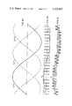
- FIG. 1 is a schematic diagram of the power circuit of a simple three phase converter with a star circuit load
- FIG. 2a is a diagram of the time dependent voltages for zero auxiliary time dependent voltage
- FIG. 2b is a graph of the output voltage of a first converter phase plotted against time
- FIG. 2c is a graph showing the voltage of the corresponding first load phase against time
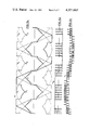
- FIG. 3c shows the curve of the voltage u 1 of the corresponding load phase
- FIG. 4b shows the curve of the time dependent voltage u 10 of the output voltage of one load phase
- FIG. 4c shows the time dependent voltage u 1 of the corresponding load phase
- FIG. 5b shows the curve of the time dependent output voltage u 10 of one load phase
- FIG. 5c shows the time dependent voltage u 1 along the corresponding load
- FIG. 6b shows the curve of the time dependent output voltage u 10 of one load phase
- FIG. 6c shows the time dependent voltage u 1 measured along the corresponding load phase
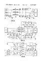
- FIG. 7a is an example of a circuit to be used for generating modulating time dependent voltages m 1 , m 2 , m 3 shown in FIGS. 3a-3c;
- FIG. 7b is an example of a circuit to be used for generating modulating time dependent voltages m 1 , m 2 , m 3 shown in FIGS. 4a-4c, or FIGS. 5a-5c;
- FIG. 7c is an example of a circuit to be used for generating modulating time dependent voltages m 1 , m 2 , m 3 shown in FIGS. 6a-6c.
- the voltage s 1 of a first phase is shown as a solid line
- the voltage small s 2 of a second phase is shown as a dash line
- the voltage s 3 of a third phase is shown as a dot-dash line.
- pulse duration modulated includes the concepts of pulse duration modulated, pulse width modulated and pulse length modulated as they are used in the field.
- the three time dependent output voltages are labeled u 10 , u 20 , u 30 .
- the load impedance is designated as Z in FIG. 1 for each load of a star group for the three phase output of the converter.
- the voltages measured along the loads are shown as u 1 , u 2 , u 3 .
- the circuit diagram of FIG. 1 shows the power circuit of a simple three phase converter where the circuits for forced commutation are omitted for clarity.
- the voltages u 10 , u 20 , u 30 are output voltages of the several phases of the converter measured against the medium of the input voltage u d FIG.
- the desired sinusoidal time dependent voltages along the load s 1 , s 2 , s 3 are in this case identical with the modulating time dependent voltages m 1 , m 2 , m 3 for effecting the pulse duration modulation, and resulting in the varying widths of the pulses of the output voltages u 10 , u 20 , u 30 .
- This modulation can be performed directly with identical carrier frequency for all phases according to a comparison of the modulating time dependent voltage with the triangle voltage.
- FIG. 2b shows the curve of the output voltage u 10 of a converter phase
- FIG. 2c shows the curve of a voltage u 1 of the corresponding load phase and wherein waves are excluded which do not form part of a three phase system.
- FIGS. 3a, 3b, and 3c show an example wherein the auxiliary time dependent voltage is set by the formula having the momentary value of the voltage d equal to the negative half of the sum of the momentary value of the desired sinusoidal time dependent voltages along the load s 1 , s 2 , s 3 , which has the largest value at that moment and of the voltage which has the smallest (negative) value at the same moment.
- auxiliary time dependent voltage d can be expressed as follows:
- FIGS. 4a, 4b, and 4c represent the situation where the auxiliary time dependent voltage d is set at each moment of time by the difference between the maximum modulating value which can be attained and which is designated as M and the momentary value of one of the desired time dependent voltages s 1 , s 2 , s 3 having at that moment of time the largest absolute value and giving the resulting value the same sign as that of the particular time dependent voltage s i which enters into the formation of the difference.
- the absolute value of s i is designated as as S 1 /
- the auxiliary time dependent voltage d of FIG. 4 can be expressed by the formula:
- Sign (max/S 1 , S 2 , S 3 /) refers to the sign of that desired time dependent voltage s i , the absolute value of which is the largest at that moment of time.
- FIG. 4b shows the curve of the time dependent voltage u 10 of the output voltage of one load phase and FIG. 4a shows the time dependent voltage u 1 of the corresponding load phase.
- FIGS. 5a, 5b, and 5c show the situation, where the auxiliary time dependent voltage d is formed by the difference between the maximum attainable modulating voltage M and that of the desired dependent voltages s i of the load phases having at the moment of time the second largest absolute value and giving the difference the same sign as the voltage having the second largest absolute value.
- the auxiliary time dependent voltage can be expressed by the formula:
- FIG. 5b shows the curve of the time dependent output voltage u 10 of one load phase and FIG. 5c shows the time dependent voltage u 1 along the corresponding load.
- FIG. 6b shows the curve of the time dependent output voltage u 10 of one load phase and in FIG. 6c the time dependent voltage u 1 measured along the corresponding load phase.
- FIG. 7a relating to the wave forms in FIGS. 3a-3c, a source of the desired sinusoidal time dependent voltages s 1 , s 2 and s 3 (FIG. 3) corresponding to the desired wave forms of voltages u 1 , u 2 , u 3 on the inverter load phases (FIG. 1), is shown, quite in general, as three voltage sources S 1 , S 2 , S 3 the voltages of which are related to common earth potential.
- the block PM designates a pulse width modulator, viz.
- inverter of input analog signals here voltages
- input analog signals here voltages
- Z 1 , Z 2 , Z 3 for inverting said signals into pulse width signals to be further availed of for selecting the on- and off-switch instants of thyristors of the inverter shown in FIG. 1.
- the voltage sources S 1 , S 2 , S 3 would be immediately connected to the input terminals Z 1 , Z 2 , Z 3 of the modulator PM.
- Diodes D1 through D6 together with resistors R1 and R2 of the same resistance and with the three phase adding transformer TF are designed for generating a time dependent auxiliary voltage d (see FIG.
- FIG. 7b shows an example of circuit wherein to the desired sinusoidal waveforms s 1 , s 2 , s 3 the auxiliary time dependent voltage d in accordance with FIG. 4a is added, or that of FIG. 5a if the inverting and the non-inverting inputs of operation amplifier OA4 are exchanged.
- the block S stands for three voltage sources S 1 , S 2 , S 3 as shown in FIG. 7a while the block PM denotes again the modulator.
- the voltage at the auxiliary output Z 4 of the modulator PM represents the positive value plus M of the maximum modulating voltage M (see FIGS. 4 to 6, incl.).
- M the maximum modulating voltage M
- said limit value corresponds to a positive amplitude of auxiliary sawtooth voltage which is compared in the modulator with the input analog voltage.
- the negative value minus M of the maximum modulating voltage M is accessible.
- the part of the circuitry consisting of operation amplifiers OA1, OA2, OA3 and OA4 interconnected as comparators, and of resistors R1, R2, R3, and R4 determines the instantaneous polarity of the auxiliary time dependent voltage d whereas the part of the circuit comprising operation amplifiers OA5 through OA10, diodes D1 through D6 and the adding transformer TF determines the instantaneous magnitude of the auxiliary time dependent voltage d shown in FIG. 4a.
- the auxiliary time dependent voltage d and, m 1 , m 2 , m 3 will correspond to those shown in FIG. 5a.
- FIG. 7c represents an example of circuit designed to obtain the pulse width modulation variant shown in FIG. 6.
- the significance of the blocks S and PM as well as of terminals Z1 through Z4 is the same as in FIG. 7b.
- this circuit modification makes use of adders constituted by the operating amplifiers OA1 through OA3 and the resistors R1 through R12.
- the circuit comprising the operation amplifier OA4, the diodes D1 through D4 and the resistors R13 and R14 generates the inverted auxiliary time dependent voltage d shown in FIG. 6a.
- FIGS. 7a, 7b, and 7c To demonstrate the variability of practical circuit implementations of the claimed method of pulse width modulation, various circuitry principles have been availed of for fulfilling the same partial functions as shown in FIGS. 7a, 7b, and 7c.
- FIGS. 7a, 7b, and 7c For adding the voltages S 1 , S 2 , S 3 to the auxiliary d there are designed mutually interchangeable adding transformer TF (FIGS. 7a and 7b) and an adder based upon operation amplifiers; one possible connection of the adder is demonstrated by the circuit in FIG. 7c.
- a sectional circuit (FIG. 7c) comprising the operation amplifier OA4, the diodes D1 through D4 and the resistors R13 and R14 is replaceable by a sectional circuit (FIG.
- FIG. 7b consisting of operation amplifiers OA5 through OA7 and the diodes D1 through D3, provided that the node of resistors R7 through R9 (FIG. 7c) is connected, via a resistor, to a sufficiently high positive potential.
- the above-mentioned sectional circuit shown in FIG. 7c could replace, admittedly with a lower exactness, the above sectional circuit shown in FIG. 7b, provided that the output of the operation amplifier OA4 is connected via a diode.
- the operation amplifiers OA8 through OA10 (FIG. 7b) can be replaced.
- a diode rectifier (FIG. 7a) consisting of the diodes D1 through D6 can be replaced by a well-known connection of an ideal dropless rectifier based upon operation amplifiers and diodes.
- circuits in which physical carriers of the time dependent waveforms as shown in FIGS. 3-6, incl., are constituted by instantaneous voltage magnitudes Such circuits are instructive and yet usual in technical practice.
Landscapes
- Engineering & Computer Science (AREA)
- Power Engineering (AREA)
- Inverter Devices (AREA)
- Ac-Ac Conversion (AREA)
- Dc-Dc Converters (AREA)
Applications Claiming Priority (2)
| Application Number | Priority Date | Filing Date | Title |
|---|---|---|---|
| CS7600004319A CS185455B1 (en) | 1976-06-30 | 1976-06-30 | Method of puls width modulation |
| CS4319-76 | 1976-06-30 |
Related Parent Applications (1)
| Application Number | Title | Priority Date | Filing Date |
|---|---|---|---|
| US05811888 Continuation-In-Part | 1977-06-30 |
Publications (1)
| Publication Number | Publication Date |
|---|---|
| US4321663A true US4321663A (en) | 1982-03-23 |
Family
ID=5385656
Family Applications (1)
| Application Number | Title | Priority Date | Filing Date |
|---|---|---|---|
| US06/041,343 Expired - Lifetime US4321663A (en) | 1976-06-30 | 1979-05-22 | Process of pulse duration modulation of a multi-phase converter |
Country Status (6)
| Country | Link |
|---|---|
| US (1) | US4321663A (cs) |
| CS (1) | CS185455B1 (cs) |
| DD (1) | DD130086A1 (cs) |
| DE (1) | DE2719989C2 (cs) |
| SE (1) | SE441882B (cs) |
| SU (1) | SU881996A1 (cs) |
Cited By (9)
| Publication number | Priority date | Publication date | Assignee | Title |
|---|---|---|---|---|
| US4458194A (en) * | 1981-11-04 | 1984-07-03 | Eaton Corporation | Method and apparatus for pulse width modulation control of an AC induction motor |
| US4642748A (en) * | 1985-08-29 | 1987-02-10 | Mai Basic Four, Inc. | Monitoring switch mode converter performance utilizing duty cycle |
| US4656572A (en) * | 1985-02-19 | 1987-04-07 | Westinghouse Electric Corp. | PWM inverter |
| US5168437A (en) * | 1990-11-13 | 1992-12-01 | Westinghouse Electric Corp. | Phase displaced, multiple inverter bridge circuits with waveform notching for harmonic elimination |
| US5631819A (en) * | 1995-04-17 | 1997-05-20 | Hitachi, Ltd. | Power converter |
| US5990657A (en) * | 1996-02-29 | 1999-11-23 | Hitachi, Ltd. | Inverter system and control system for electric vehicle |
| US20090058330A1 (en) * | 2007-08-30 | 2009-03-05 | Seagate Technology Llc | Driving a multi-phased motor |
| US7728451B2 (en) | 2006-12-14 | 2010-06-01 | Hitachi, Ltd. | Wind power generation system |
| US20100302085A1 (en) * | 2007-09-28 | 2010-12-02 | Siemens Ag | Field Device Having an Analog Output |
Families Citing this family (2)
| Publication number | Priority date | Publication date | Assignee | Title |
|---|---|---|---|---|
| JPS5622595A (en) * | 1979-07-28 | 1981-03-03 | Toshiba Mach Co Ltd | Controller for torque of induction motor |
| DE2945145A1 (de) * | 1979-11-06 | 1981-05-14 | Licentia Patent-Verwaltungs-Gmbh, 6000 Frankfurt | Verfahren zur verminderung des steuerblindleistungsbedarfs |
Citations (3)
| Publication number | Priority date | Publication date | Assignee | Title |
|---|---|---|---|---|
| US3603867A (en) * | 1969-06-09 | 1971-09-07 | Battelle Memorial Institute | Method of controlling a polyphase inverter |
| US3624486A (en) * | 1970-03-06 | 1971-11-30 | Westinghouse Electric Corp | Apparatus for controlling pulse width modulation of inverter circuits |
| US3886431A (en) * | 1973-12-06 | 1975-05-27 | Reliance Electric Co | Synchronizing circuit having an infinite number of ratios |
Family Cites Families (2)
| Publication number | Priority date | Publication date | Assignee | Title |
|---|---|---|---|---|
| AT232134B (de) * | 1962-02-12 | 1964-03-10 | Asea Ab | Steueranordnung für Umrichter |
| DE2345035C2 (de) * | 1973-09-06 | 1975-10-23 | Siemens Ag, 1000 Berlin Und 8000 Muenchen | Verfahren und Anordnung zur Steuerung oder Regelung der Drehzahl einer umrichtergespeisten dreiphasigen Drehfeldmaschine |
-
1976
- 1976-06-30 CS CS7600004319A patent/CS185455B1/cs unknown
-
1977
- 1977-05-04 DE DE2719989A patent/DE2719989C2/de not_active Expired
- 1977-05-10 SE SE7705467A patent/SE441882B/xx not_active IP Right Cessation
- 1977-06-07 SU SU772489909A patent/SU881996A1/ru active
- 1977-06-24 DD DD7700199688A patent/DD130086A1/xx not_active IP Right Cessation
-
1979
- 1979-05-22 US US06/041,343 patent/US4321663A/en not_active Expired - Lifetime
Patent Citations (3)
| Publication number | Priority date | Publication date | Assignee | Title |
|---|---|---|---|---|
| US3603867A (en) * | 1969-06-09 | 1971-09-07 | Battelle Memorial Institute | Method of controlling a polyphase inverter |
| US3624486A (en) * | 1970-03-06 | 1971-11-30 | Westinghouse Electric Corp | Apparatus for controlling pulse width modulation of inverter circuits |
| US3886431A (en) * | 1973-12-06 | 1975-05-27 | Reliance Electric Co | Synchronizing circuit having an infinite number of ratios |
Cited By (11)
| Publication number | Priority date | Publication date | Assignee | Title |
|---|---|---|---|---|
| US4458194A (en) * | 1981-11-04 | 1984-07-03 | Eaton Corporation | Method and apparatus for pulse width modulation control of an AC induction motor |
| US4656572A (en) * | 1985-02-19 | 1987-04-07 | Westinghouse Electric Corp. | PWM inverter |
| US4642748A (en) * | 1985-08-29 | 1987-02-10 | Mai Basic Four, Inc. | Monitoring switch mode converter performance utilizing duty cycle |
| US5168437A (en) * | 1990-11-13 | 1992-12-01 | Westinghouse Electric Corp. | Phase displaced, multiple inverter bridge circuits with waveform notching for harmonic elimination |
| US5631819A (en) * | 1995-04-17 | 1997-05-20 | Hitachi, Ltd. | Power converter |
| US5990657A (en) * | 1996-02-29 | 1999-11-23 | Hitachi, Ltd. | Inverter system and control system for electric vehicle |
| JP3259626B2 (ja) | 1996-02-29 | 2002-02-25 | 株式会社日立製作所 | インバータ装置および電気車制御装置 |
| US7728451B2 (en) | 2006-12-14 | 2010-06-01 | Hitachi, Ltd. | Wind power generation system |
| CN101207289B (zh) * | 2006-12-14 | 2012-06-13 | 株式会社日立制作所 | 风力发电装置 |
| US20090058330A1 (en) * | 2007-08-30 | 2009-03-05 | Seagate Technology Llc | Driving a multi-phased motor |
| US20100302085A1 (en) * | 2007-09-28 | 2010-12-02 | Siemens Ag | Field Device Having an Analog Output |
Also Published As
| Publication number | Publication date |
|---|---|
| DD130086A1 (de) | 1978-03-01 |
| CS185455B1 (en) | 1978-09-15 |
| SU881996A1 (ru) | 1981-11-15 |
| SE7705467L (sv) | 1977-12-31 |
| DE2719989C2 (de) | 1986-08-07 |
| SE441882B (sv) | 1985-11-11 |
| DE2719989A1 (de) | 1978-01-05 |
Similar Documents
| Publication | Publication Date | Title |
|---|---|---|
| US3742330A (en) | Current mode d c to a c converters | |
| US6023417A (en) | Generalized discontinuous pulse width modulator | |
| AU701174B2 (en) | Opposed current power converter | |
| US5610806A (en) | Pulse width modulation method for driving three phase power inverter/converter switches with balanced discontinuous phase commands | |
| US4321663A (en) | Process of pulse duration modulation of a multi-phase converter | |
| US5021936A (en) | PWM power converter using mixed bipolar and static induction transistors | |
| Holtz et al. | Reduced harmonics PWM controlled line-side converter for electric drives | |
| KR950022005A (ko) | 전력변환장치 | |
| SE307616B (cs) | ||
| US4914396A (en) | PWM waveform generator | |
| JPH09308256A (ja) | Pwmインバータ装置 | |
| RU2389128C1 (ru) | Способ формирования широтно-импульсных сигналов управления автономного инвертора | |
| JPH0799782A (ja) | 平頂波形発生器及びそれを用いたパルス幅変調器 | |
| RU2020737C1 (ru) | Способ многоканального широтно-импульсного преобразования аналогового сигнала и устройство для его осуществления | |
| JPH0898540A (ja) | Pwmインバータ | |
| RU2025879C1 (ru) | Способ управления автономным инвертором с широтно-импульсной модуляцией | |
| JPH09163754A (ja) | 直列多重型インバータの制御装置 | |
| SU792238A1 (ru) | Стабилизированный преобразователь | |
| Keskar et al. | A fuzzy controller for extending linearity of overmodulated PWM waveform | |
| RU2025877C1 (ru) | Способ управления преобразователем трехфазного напряжения в постоянное | |
| RU2007847C1 (ru) | Многоканальный ключевой усилитель | |
| RU1818688C (ru) | Способ многоканального широтно-импульсного преобразовани аналогового сигнала и устройство дл его осуществлени | |
| JPH01138965A (ja) | 直流電源装置 | |
| RU2046528C1 (ru) | Способ управления следящим импульсным преобразователем | |
| DE2719290C3 (de) | Wechselrichteranordnung |
Legal Events
| Date | Code | Title | Description |
|---|---|---|---|
| STCF | Information on status: patent grant |
Free format text: PATENTED CASE |