US4197486A - Control system for deflecting an electron beam - Google Patents
Control system for deflecting an electron beam Download PDFInfo
- Publication number
- US4197486A US4197486A US05/842,155 US84215577A US4197486A US 4197486 A US4197486 A US 4197486A US 84215577 A US84215577 A US 84215577A US 4197486 A US4197486 A US 4197486A
- Authority
- US
- United States
- Prior art keywords
- electron beam
- output
- signal
- control system
- deflection
- Prior art date
- Legal status (The legal status is an assumption and is not a legal conclusion. Google has not performed a legal analysis and makes no representation as to the accuracy of the status listed.)
- Expired - Lifetime
Links
Images


Classifications
-
- G—PHYSICS
- G09—EDUCATION; CRYPTOGRAPHY; DISPLAY; ADVERTISING; SEALS
- G09G—ARRANGEMENTS OR CIRCUITS FOR CONTROL OF INDICATING DEVICES USING STATIC MEANS TO PRESENT VARIABLE INFORMATION
- G09G1/00—Control arrangements or circuits, of interest only in connection with cathode-ray tube indicators; General aspects or details, e.g. selection emphasis on particular characters, dashed line or dotted line generation; Preprocessing of data
- G09G1/06—Control arrangements or circuits, of interest only in connection with cathode-ray tube indicators; General aspects or details, e.g. selection emphasis on particular characters, dashed line or dotted line generation; Preprocessing of data using single beam tubes, e.g. three-dimensional or perspective representation, rotation or translation of display pattern, hidden lines, shadows
- G09G1/08—Control arrangements or circuits, of interest only in connection with cathode-ray tube indicators; General aspects or details, e.g. selection emphasis on particular characters, dashed line or dotted line generation; Preprocessing of data using single beam tubes, e.g. three-dimensional or perspective representation, rotation or translation of display pattern, hidden lines, shadows the beam directly tracing characters, the information to be displayed controlling the deflection and the intensity as a function of time in two spatial co-ordinates, e.g. according to a cartesian co-ordinate system
Definitions
- This invention relates to an electron beam deflection control system which is suitable for use in an electron beam exposure system, a graphic display system, and the like.
- An electron beam exposure system functions to form a minute pattern of a semiconductor device or circuit on a mask or a semiconductor wafer with an electron beam.
- the system employs an electron beam deflection control circuit which deflects the electron beam linearly at a uniform speed and which, upon completion of the drawing of one pattern, cuts off the electron beam and moves it to the starting point of the next pattern.
- the electron beam deflection control system of this type has been provided as a digital system and an analog system in the prior art.
- coordinate data corresponding to respective points of a line pattern are sequentially generated in accordance with data fed from a digital computer, they are converted into an analog signal having a stepped shape by a digital-to-analog converter, and the electron beam is deflected stepwise.
- a digital-to-analog converter which determines each step width of the stepped signal is long. Disadvantageously, therefore, as the line pattern becomes longer, the drawing time becomes longer.
- a closed loop circuit consisting of a differential amplifier having a limiter function and an integrator is provided, start point and end point levels of a drawing pattern generated by a digital-to-analog converter are sequentially impressed on the closed loop circuit, and the outputs of the integrator are converged to the end point level, thereby to produce a triangular deflection signal.
- the outputs of the integrator becomes dull in the vicinity of the start and end points of the drawing patern, and therefore, degrade the precision of the drawing pattern.
- the convergence time of the first-order lag system formed by the differential amplifier and the integrator increases as a dead time. Therefore, in the case where the drawing pattern is short, the dead time becomes significant as compared with the drawing time. Since the triangular deflection signal is used also for the movement of the beam between the patterns, the dead time increases still more.
- An object of this invention is to provide an electron beam deflection control system which makes it possible to execute a drawing at a very high speed.
- Another object of this invention is to provide an electron beam deflection control system which enhances the precision of a drawing pattern.
- this invention consists in changing over and operating an analog system which generates a triangular deflection signal varying at a comparatively low speed and a digital system which generates a stepped deflection signal varying at a comparatively high speed.
- the digital and analog systems are changed over by taking notice of the fact that, in the digital system, the length of a pattern to be drawn and the drawing speed are in perfect proportional relation, yet the gradient of a proportional curve is great by reason of the setting time of the digital-to-analog converter described previously; while, in the analog system, the length of a drawing pattern and the drawing speed are in a proportional relation in the form in which a shift of the dead time described earlier is involved, yet the gradient of a proportional curve is small.
- the drawing pattern is short, the digital system has a relatively short drawing time; whereas, when the drawing pattern becomes long, the analog system has a relatively short drawing time.
- a long pattern is drawn by the analog system, and the drawing of a short pattern or the beam movement between patterns is carried out by the digital system.
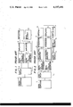
- FIG. 1 is a block diagram of a prior art charged beam deflection control system of the digital type
- FIG. 2 is a block diagram of a prior art charged beam deflection control system of the analog type
- FIGS. 3 and 3a are block diagrams which show a first embodiment of a charged beam deflection control system according to this invention.
- FIG. 4 is an operating time chart of the embodiment of FIG. 3 operating as an analog system
- FIG. 5 is an operating time chart of the embodiment of FIG. 3 operating as a digital system
- FIGS. 6(a) and 6(b) are a block diagram and a characteristic diagram, respectively, which illustrate a second embodiment of the charged beam deflection control system according to this invention.
- FIG. 7 shows an example of a pattern drawn by the embodiment of FIGS. 6(a) and 6(b).
- FIG. 1 shows the block arrangement of a prior art beam deflection control system of the digital type.
- Numeral 1 designates a digital computer
- numeral 2 a logic circuit for producing a control signal
- numerals 3 and 4 digital-to-analog converters
- numerals 5 and 6 amplifiers for amplifying deflection signals
- numeral 7 a deflector
- numeral 8 a beam blanker.
- coordinate data corresponding to respective points of a pattern are sequentially produced by the logic circuit 2 in accordance with data fed from the digital computer 1.
- the resultant data is converted into analog signals (voltages or currents) by the digital-to-analog converters 3 and 4.
- the converter 3 and the amplifier 5 form the x-direction channel
- the converter 4 and the amplifier 6 form the y-direction channel.
- the analog signals are in a stepped shape, a beam is deflected stepwise.
- the time at which the step is advanced is controlled by a signal of a clock generator contained within the logic circuit 2.
- a beam blanking signal can be digitally generated by the logic circuit 2.
- the digital-to-analog converter 3 or 4 is controlled by the logic circuit 2 so that the beam may arrive at a target point in one block.
- the precision of the drawing pattern is excellent.
- the system has a disadvantage as stated below.
- the width of each step of the stepped signal is determined by the settling time of the digital-to-analog converter. In general, the settling time is long; therefore, as the drawing pattern becomes longer, the drawing time becomes longer proportionally.
- the system of this type is accordingly very inconvenient for drawing a long pattern.
- FIG. 2 shows a block diagram of a prior art beam deflection control system of the analog type. Elements 1 through 8 are the same as those components designated by corresponding symbols in FIG. 1. Numerals 9 and 10 indicate differential amplifiers with voltage limiters, numeral 11 a logic circuit for beam blanking signal generation and containing a voltage comparator therein, and numerals 12 and 13 integrators.
- the output of the differential amplifier 9 When the output of the integrator 12 has come to the output of the converter 3, the output of the differential amplifier 9 enters a linear region, and the first order lag circuit composed of the differential amplifier 9 and the integrator 12 converges to a point at which the output of the converter 3 and that of the differential amplifier 9 coincide. At this time, the output of the differential amplifier 9 becomes zero. It is detected by the voltage comparator contained in the logic circuit 11, and a beam OFF signal is provided at the output of the logic circuit 11 so as to blank the beam. This process is repeated, and the scanning and drawing is done by triangular waves. The y-directional deflection is similarly executed by the converter 4, the operational amplifier 10 and the integrator 13.
- the disadvantages of this system are that the output of the integrator 12 becomes dull in the vicinities of the start and end points of the line to degrade the quality of the drawing pattern, and that the convergence time of the first order lag system constituted of the differential amplifier 9 and the integrator 12 increases as a dead time. Especially, when the length of the drawing line becomes less than about 10 ⁇ m, the dead time becomes significant in comparison with the drawing time. Besides, it leads to an increase of the dead time to carry out the beam movement under the beam blanking state by the use of the triangular wave signal.
- FIG. 3 shows an embodiment of an electron beam deflection control system according to this invention. Elements 1, 2, 3, 5, 7, 8, and 12 correspond to those components identified by the same symbols in FIGS. 1 and 2.
- Numeral 14 designates a voltage generator for determining the line speed, numeral 15 a polarity change-over circuit for changing over the polarity of the output from the voltage generator 14, numeral 16 an analog switch, numeral 17 a logic circuit for beam blanking signal generation, numeral 18 a differential amplifier, numeral 19 a zero detector, and numeral 20 a sample and hold circuit. Except for the digital computer 1, logic circuit 2, and beam blanker 8, the components corresponding to one axis (x-axis or y-axis) are illustrated in FIG. 3. The same construction applies to the other axis.
- an analog output signal 31 corresponding to the starting point of the line is generated by the converter 3 in response to the digital computer 1 and the logic circuit 2.
- the sample and hold circuit 20 is set at a sampling mode in advance, and the output signal 31 is applied to a first input terminal of the differential amplifier 18. Since an output signal 121 from the integrator 12 is applied to a second input terminal of the differential amplifier 18, an output 181 from the differential amplifier 18 represents gain times and voltage difference between the output signals 31 and 121.
- the data representing the end point of the line is applied to the converter 3, and an output signal 31 of an analog voltage corresponding to the end point is generated.
- the analog switch 16 is changed over from the side of the differential amplifier 18 to the side of the polarity change-over circuit 15 by a control signal 23 from the logic circuit 2.
- the integrating operation of the integrator 12 is initiated in conformity with the line speed set by the voltage generator 14 and the polarity set by the polarity change-over circuit 15, and the output signal 121 varies linearly versus time.
- the logic circuit 17 is rendered operative by a control signal 24, and an output signal 171 in the form of a beam blanking signal is switched to the beam ON state, to start the drawing operation.
- the sample and hold circuit 20 is changed over from the holding mode to the sampling mode by the control signal 22 from the logic circuit 2, and the output signal 31 is applied to the differential amplifier 18.
- the output signal 121 coincides with the output signal 31, the output 181 becomes zero, the zero detector 19 becomes operative, and an output signal 191 rises.
- the AND operation between the output signal 191 and the ON state of the signal 171 is taken, and the output signal 171 being the beam blanking signal is switched to the beam OFF state by the logic circuit 17, so that the drawing operation is stopped.
- a control signal 24' from the logic circuit 17 is applied to the logic circuit 2, the analog switch 16 is changed over to the side of the differential amplifier 18 by the control signal 23, and a closed loop consisting of the analog switch 16, the integrator 12 and the differential amplifier 18 is established so as to bring the output signal 121 to the same level as that of the output signal 31.
- the output signal 121 is brought to the next start point level at a time t 5 and returns to a steady state at t 6 .
- the output signal 121 is amplified by the deflector 7, to deflect the beam.
- the pattern can be drawn as a set of lines. In this manner, the triangular wave signal is used for drawing the long line, whereby a higher speed than in the digital system is achieved.
- the time in which the output signal 121 follows up the output signal 31 is determined by (integration time-constant of the integrator 12)/(gain of the differential amplifier 18), and the drawing speed is rendered high. Meanwhile, the logic circuit 17 is inhibited by a control signal 24 so as not to operate, and the output signal 171 remains "off.”
- the sample and hold circuit 20 is set at the sampling mode by a control signal 22, while the analog switch 16 is connected to the side of the differential amplifier 18 by a control signal 23. Accordingly, the output signal 121 follows up the output signal 31 with high speed.
- the output signal 31 is similarly shifted and settled to a level corresponding to the position of a third dot.
- the line is drawn as a row of dots.
- Whether the digital system or the analog system is to be used may be determined by operating the logic circuits contained in the block 2 in conformity with the data fed from the digital computer 1 and thus controlling the control signals 22, 23, and 24 as well as the input signal of the digital-to-analog converter 3.
- FIG. 3a illustrates one embodiment of concrete construction of the logical circuit 2 shown in FIG. 3.
- numeral 51 designates a decoder for converting the digital data 52 from the digital computer 1 into coordinate data 53 corresponding to respective points of a pattern and a mode signal 54 illustrative of an analog system or digital system
- numeral 55 a clock generator for generating clock signals 56
- numeral 57 a sequencer with counters for sequencially generating various control signals in response to the clock signal 56
- numeral 58 a target point register for storing the coordinate data and for outputting these data as signals 59, 60 and 61 in response to control signals 62 from the sequencer 57
- numeral 63 a start point register for storing the signal 61 and for outputting a start point signal 64
- numeral 65 a comparator for comparing the signal 60 representing the end point of the line pattern with the signal 64 representing the start point thereof and for generating a signal 21 for controlling the polarity of the polarity change-over circuit 15 in response to the relative magnitude of these signals 60 and 64
- numeral 66 a flip-flop circuit which is
- FIGS. 6(a) and 6(b) show another embodiment of the electron beam deflection control system according to this invention.
- FIG. 6(a) shows the principal portions of a deflection signal generator circuit for the X-axis or Y-axis.
- the illustrated circuit will hereunder be deemed the circuit for the X-axis.
- the deflection signal is provided with a satisfactory linearity.
- an appropriate voltage comparator may be used for monitoring the output e 1 of the differential amplifier 9 so as to control the electron beam intensity upon detection of the state
- the switch 16 is turned off. This does not change the output signal 121 because the integration current is zero under the present state.
- the X-coordinate of the next target point is applied to the digital-to-analog converter to slightly shift the Y-axial deflection signal (refer to ⁇ Y in FIG. 7).
- the switch 16 is turned on, whereby the output e O of the integrator 12 initiates deflection at uniform speed. At this time, accordingly, the electron beam is controlled to the ON state to execute the exposure.
- the output signals 31 and 121 are added through resistors 41 and 42, respectively, and the sum is amplified by a coefficient multiplier 40.
- the current obtained by dividing the output voltage of the coefficient multiplier 40 by the sum between the internal resistance of the switch 16' and the resistance of a resistor 125 is integrated by the integration capacitor 124.
- a path which extends from the input point of the operational amplifier 123 via the operation amplifier 123, resistor 42, coefficient multiplier 40, switch 16', and resistor 125 back to the afore-cited input point forms a negative feedback loop.
- c, r and k represent the capacitance of the integration capacitor, the sum of the resistance of the resistor 125, and the internal resistance of the switch 16', and the coefficient of the coefficient multiplier 40, respectively.
- the amplifier of the integrator or the coefficient multiplier 40 an ideal amplifier is assumed.
- the scanning and drawing in the analog system and the digital system can be easily accomplished by the block arrangements in FIG. 3 and FIG. 6(a). Therefore, e.g., by drawing a long pattern with the analog system with high speed and executing the beam movement between lines or between patterns with the digital system with high speed, a high-speed system can be provided. It is also possible to draw a short pattern or a pattern requiring an especially high precision by the use of the digital system.
- the second axis is moved to draw oblique lines with the digital system by means of the clock generator and the counter which are contained in the logical circuit 2. Further, it is possible to compensate for a deflection distortion or a sample rotation error.
- the system of this invention Owing to the system of this invention, there can be realized an electron beam exposure system which skillfully exploits the high drawing speed of the analog system in the case of drawing a long pattern and the high speed and high precision of the digital system in the case of drawing a short pattern and the case of moving a beam between patterns.
- the system of the invention is not limited by the conversion speed of the digital-to-analog converter. Therefore, the speediness can be achieved with a converter of low speed, and a system of high cost performance can be provided.
Landscapes
- Engineering & Computer Science (AREA)
- Radar, Positioning & Navigation (AREA)
- Remote Sensing (AREA)
- Physics & Mathematics (AREA)
- Computer Hardware Design (AREA)
- General Physics & Mathematics (AREA)
- Theoretical Computer Science (AREA)
- Electron Beam Exposure (AREA)
- Details Of Television Scanning (AREA)
Applications Claiming Priority (2)
| Application Number | Priority Date | Filing Date | Title |
|---|---|---|---|
| JP12316676A JPS5347776A (en) | 1976-10-14 | 1976-10-14 | Control system of charged particle beam deflection |
| JP51-123166 | 1976-10-14 |
Publications (1)
| Publication Number | Publication Date |
|---|---|
| US4197486A true US4197486A (en) | 1980-04-08 |
Family
ID=14853808
Family Applications (1)
| Application Number | Title | Priority Date | Filing Date |
|---|---|---|---|
| US05/842,155 Expired - Lifetime US4197486A (en) | 1976-10-14 | 1977-10-14 | Control system for deflecting an electron beam |
Country Status (6)
| Country | Link |
|---|---|
| US (1) | US4197486A (en:Method) |
| JP (1) | JPS5347776A (en:Method) |
| CA (1) | CA1105152A (en:Method) |
| DE (1) | DE2745881C2 (en:Method) |
| FR (1) | FR2368141A1 (en:Method) |
| GB (1) | GB1594476A (en:Method) |
Cited By (2)
| Publication number | Priority date | Publication date | Assignee | Title |
|---|---|---|---|---|
| US20020187172A1 (en) * | 2001-06-08 | 2002-12-12 | Philippe Reb | Colloidal metal labeled microparticles and methods for producing and using the same |
| CN118981146A (zh) * | 2024-07-25 | 2024-11-19 | 中国电子科技集团公司第四十八研究所 | 一种电子束静电偏转驱动电源 |
Families Citing this family (4)
| Publication number | Priority date | Publication date | Assignee | Title |
|---|---|---|---|---|
| US4500879A (en) * | 1982-01-06 | 1985-02-19 | Smith Engineering | Circuitry for controlling a CRT beam |
| CA1227972A (en) * | 1982-05-24 | 1987-10-13 | Francis R. Varrese | Method for joining tantalum to non-refractory materials and an apparatus utilizing such a technique |
| JPS5967203U (ja) * | 1982-10-28 | 1984-05-07 | 株式会社大岩技研 | 木工用多軸ボ−リングマシンにおけるドリル脱着用治具 |
| JPS6039464U (ja) * | 1983-08-22 | 1985-03-19 | 倉田 敏行 | フォ−ムタイ締め付け用ソケット |
Citations (2)
| Publication number | Priority date | Publication date | Assignee | Title |
|---|---|---|---|---|
| US3937879A (en) * | 1965-07-29 | 1976-02-10 | The United States Of America As Represented By The Secretary Of The Navy | Information display system having main and auxiliary sweeps |
| US4019090A (en) * | 1975-12-05 | 1977-04-19 | Motorola, Inc. | Self-stepping vertical scan system |
Family Cites Families (1)
| Publication number | Priority date | Publication date | Assignee | Title |
|---|---|---|---|---|
| DE1963454C3 (de) * | 1969-12-18 | 1973-12-06 | Universitaet Stuttgart, Vertreten Durch Das Institut Fuer Kernenergetik, 7000 Stuttgart | Generator für die Ansteuerung von Ablenkvorrichtungen in Elektronenstrahl geraten |
-
1976
- 1976-10-14 JP JP12316676A patent/JPS5347776A/ja active Granted
-
1977
- 1977-10-11 CA CA288,398A patent/CA1105152A/en not_active Expired
- 1977-10-12 DE DE2745881A patent/DE2745881C2/de not_active Expired
- 1977-10-13 FR FR7730818A patent/FR2368141A1/fr active Granted
- 1977-10-14 GB GB42935/77A patent/GB1594476A/en not_active Expired
- 1977-10-14 US US05/842,155 patent/US4197486A/en not_active Expired - Lifetime
Patent Citations (2)
| Publication number | Priority date | Publication date | Assignee | Title |
|---|---|---|---|---|
| US3937879A (en) * | 1965-07-29 | 1976-02-10 | The United States Of America As Represented By The Secretary Of The Navy | Information display system having main and auxiliary sweeps |
| US4019090A (en) * | 1975-12-05 | 1977-04-19 | Motorola, Inc. | Self-stepping vertical scan system |
Cited By (2)
| Publication number | Priority date | Publication date | Assignee | Title |
|---|---|---|---|---|
| US20020187172A1 (en) * | 2001-06-08 | 2002-12-12 | Philippe Reb | Colloidal metal labeled microparticles and methods for producing and using the same |
| CN118981146A (zh) * | 2024-07-25 | 2024-11-19 | 中国电子科技集团公司第四十八研究所 | 一种电子束静电偏转驱动电源 |
Also Published As
| Publication number | Publication date |
|---|---|
| DE2745881A1 (de) | 1978-04-20 |
| JPS5347776A (en) | 1978-04-28 |
| JPS5346695B2 (en:Method) | 1978-12-15 |
| DE2745881C2 (de) | 1984-05-03 |
| FR2368141A1 (fr) | 1978-05-12 |
| GB1594476A (en) | 1981-07-30 |
| CA1105152A (en) | 1981-07-14 |
| FR2368141B1 (en:Method) | 1981-12-04 |
Similar Documents
| Publication | Publication Date | Title |
|---|---|---|
| JP3120737B2 (ja) | 自動利得制御回路 | |
| JPH0621902B2 (ja) | ビームポジショナ | |
| CA1279732C (en) | Electron beam direct drawing device | |
| US4197486A (en) | Control system for deflecting an electron beam | |
| US4121299A (en) | Constant velocity vector generator employing absolute value amplifier circuits | |
| US4363025A (en) | Signal generating arrangements | |
| JPH0722303A (ja) | ラインジェネレータを用いた電子線描画装置 | |
| US4437008A (en) | Electron beam control system | |
| JP3448623B2 (ja) | 荷電粒子ビーム露光方法及び装置 | |
| JP3969463B2 (ja) | 荷電粒子ビーム露光方法及び装置 | |
| US4032760A (en) | Phosphor protection for x-y loops | |
| JP3584962B2 (ja) | 荷電ビーム描画方法及びその装置 | |
| JPH07107891B2 (ja) | 電子線描画装置 | |
| KR100192199B1 (ko) | 에러 신호 발생 회로 | |
| JPS58161529A (ja) | 増幅回路 | |
| SU738191A1 (ru) | Устройство цифровой развертки дл электронно-лучевых трубок | |
| JPH06151287A (ja) | 電子線描画方法および装置 | |
| JPH02234339A (ja) | 荷電ビーム描画装置 | |
| JPS6234137B2 (en:Method) | ||
| EP0169310A1 (en) | Alignment correction system | |
| JPH01196921A (ja) | アナログーデイジタル変換装置 | |
| JPH04172201A (ja) | 位置検出器およびその検出器を用いたレンズ装置 | |
| JPH05326383A (ja) | 電子ビーム露光装置 | |
| JPS58180024A (ja) | 電子ビ−ム露光方法 | |
| JPS5925371B2 (ja) | 電子ビ−ム露光方法 |
Legal Events
| Date | Code | Title | Description |
|---|---|---|---|
| AS | Assignment |
Owner name: NIPPON TELEGRAPH & TELEPHONE CORPORATION Free format text: CHANGE OF NAME;ASSIGNOR:NIPPON TELEGRAPH AND TELEPHONE PUBLIC CORPORATION;REEL/FRAME:004454/0001 Effective date: 19850718 |